Renesas RZ Series User Manual
Smarc module board
Hide thumbs
Also See for RZ Series:
- User manual (62 pages) ,
- Demonstration manual (49 pages) ,
- Quick start manual (26 pages)
Table of Contents
Advertisement
Quick Links
Cover
RZ/G2UL, RZ/A3UL, RZ/Five
SMARC Module Board
Renesas Microprocessor
RZ Family / RZ/G, RZ/A Series
RTK9743U11C01000BE
RTK9743F01C01000BE
RTK9763U02C01000BE
RTK9763U02C01001BE
All information contained in these materials, including products and product specifications,
represents information on the product at the time of publication and is subject to change by
Renesas Electronics Corp. without notice. Please review the latest information published by
Renesas Electronics Corp. through various means, including the Renesas Electronics Corp.
website (http://www.renesas.com).
www.renesas.com
User's Manual: Hardware
Rev.1.01 Jul, 2022
1 Renesas Electronics Corporation. All rights reserved.
Advertisement
Table of Contents

Related Manuals for Renesas RZ Series


Summary of Contents for Renesas RZ Series
- Page 1 All information contained in these materials, including products and product specifications, represents information on the product at the time of publication and is subject to change by Renesas Electronics Corp. without notice. Please review the latest information published by Renesas Electronics Corp. through various means, including the Renesas Electronics Corp.
- Page 2 Renesas Electronics disclaims any and all liability for any damages or losses incurred by you or any third parties arising from the use of any Renesas Electronics product that is inconsistent with any Renesas Electronics data sheet, user’s manual or other Renesas Electronics document.
- Page 3 Note that in each section of the Manual, trademark notation of ® and TM may be omitted. All other trademarks and registered trademarks are the property of their respective owners. AndesCore™ AX45MP is a trademark owned by Andes Technology Corporation. © 2022 Renesas Electronics Corporation. All rights reserved.
- Page 4 Microcontroller Unit Products The following usage notes are applicable to all Microprocessing unit and Microcontroller unit products from Renesas. For detailed usage notes on the products covered by this document, refer to the relevant sections of the document as well as any technical updates that have been issued for the products.
-
Page 5: Table Of Contents
Table of Contents Overview ........................7 Overview ............................7 Configuration ............................ 8 Features ............................9 1.3.1 RTK9743U11C01000BE (RZ/G2UL SMARC Module Board) ..........9 1.3.2 RTK9763U02C01000BE (RZ/A3UL SMARC Module Board QSPI Edition) ......10 1.3.3 RTK9763U02C01001BE (RZ/A3UL SMARC Module Board OCTAL Edition) ..... 11 1.3.4 RTK9743F01C01000BE (RZ/Five SMARC Module Board) .......... - Page 6 2.11.2 SD Card ..........................56 2.12 GreenPAK ............................57 2.13 Parallel Output Interface ......................... 58 Operation Specifications ..................... 59 Overview of Connectors ......................... 59 3.1.1 ADC Connector (CN1) ......................60 3.1.2 JTAG Connector (CN2) ......................61 3.1.3 MicroSD Card Slot (CN3) ..................... 62 3.1.4 SMARC edge Connector (CN4) ...................
-
Page 7: Overview
Overview This document describes a specification of the RZ/G2UL, RZ/A3UL and RZ/Five SMARC Module Board to evaluate the functions and performance of the Renesas Electronics microprocessor RZ/G2UL “R9A07G043U11GBG”, RZ/A3UL “R9A07G063U02GBG” and RZ/Five “R9A07G043F01GBG” and evaluate application software programs. This document introduces 4 types of the SMARC Module Boards. -
Page 8: Configuration
RZ Family / RZ/G, RZ/A Series 1. Overview Configuration Figure 1.1 shows an example of system configuration using the RTK9743U11C01000BE. RZ/G2UL SMARC Module Board RTK9743U11C01000BE Power supply through RZ/G2UL USB Type-C AC adapter(*1) RZ SMARC Series Carrier Board Host computer RTK97X4XXXB00000BE SCIF download (*1): Should be procured on the customer side... -
Page 9: Features
RZ Family / RZ/G, RZ/A Series 1. Overview Features 1.3.1 RTK9743U11C01000BE (RZ/G2UL SMARC Module Board) Table 1.1 shows the features of the RTK9743U11C01000BE. Table 1.1 Features of the RTK9743U11C01000BE Item Details RZ/G2UL Input (Xin) clock: 24MHz Arm Cortex-A55 clock: 1.0GHz Arm Cortex-M33 clock: 200MHz AXI-bus clock: 200MHz APB-bus clock: 100MHz... -
Page 10: Rtk9763U02C01000Be (Rz/A3Ul Smarc Module Board Qspi Edition)
RZ Family / RZ/G, RZ/A Series 1. Overview 1.3.2 RTK9763U02C01000BE (RZ/A3UL SMARC Module Board QSPI Edition) Table 1.2 shows the features of the RTK9763U02C01000BE. Table 1.2 Features of the RTK9763U02C01000BE Item Details RZ/A3UL Input (Xin) clock: 24MHz Arm Cortex-A55 clock: 1.0GHz AXI-bus clock: 200MHz APB-bus clock: 100MHz Internal memory... -
Page 11: Rtk9763U02C01001Be (Rz/A3Ul Smarc Module Board Octal Edition)
RZ Family / RZ/G, RZ/A Series 1. Overview 1.3.3 RTK9763U02C01001BE (RZ/A3UL SMARC Module Board OCTAL Edition) Table 1.3 shows the features of the RTK9763U02C01001BE. Table 1.3 Features of the RTK9763U02C01001BE Item Details RZ/A3UL Input (Xin) clock: 24MHz Arm Cortex-A55 clock: 1.0GHz AXI-bus clock: 200MHz APB-bus clock: 100MHz Internal memory... -
Page 12: Rtk9743F01C01000Be (Rz/Five Smarc Module Board)
RZ Family / RZ/G, RZ/A Series 1. Overview 1.3.4 RTK9743F01C01000BE (RZ/Five SMARC Module Board) Table 1.4 shows the features of the RTK9743F01C01000BE. Table 1.4 Features of the RTK9743F01C01000BE Item Details RZ/Five Input (Xin) clock: 24MHz AndesCore AX45MP clock: 1.0GHz AXI-bus clock: 200MHz APB-bus clock: 100MHz Internal memory Instruction cache: 32KB... -
Page 13: Physical View
RZ Family / RZ/G, RZ/A Series 1. Overview Physical View Figure 1.2 and Figure 1.3 show the top and bottom views of the RTK9743U11C01000BE. Figure 1.2 Top View of the RTK9743U11C01000BE NOTE This picture is of the RTK9743U11C01000BE. R01UH0990EJ0101 Rev.1.01 Page 13 of 83 Jul 28, 2022... - Page 14 RZ Family / RZ/G, RZ/A Series 1. Overview Figure 1.3 Bottom View of the RTK9743U11C01000BE NOTE This picture is of the RTK9743U11C01000BE. R01UH0990EJ0101 Rev.1.01 Page 14 of 83 Jul 28, 2022...
-
Page 15: Block Diagram
RZ Family / RZ/G, RZ/A Series 1. Overview Block Diagram 1.5.1 RTK9743U11C01000BE (RZ/G2UL SMARC Module Board) Figure 1.4 shows the block diagram of the RTK9743U11C01000BE. RTK9743U11C01000BE SCIF0 RZ/G2UL SDHI1 DDR4 SDRAM USB0 OTG USB1 Host ANALOG CSI-2 QSPI SPI Multi I/O flash CAN0 CAN1... -
Page 16: Rtk9763U02C01000Be (Rz/A3Ul Smarc Module Board Qspi Edition)
RZ Family / RZ/G, RZ/A Series 1. Overview 1.5.2 RTK9763U02C01000BE (RZ/A3UL SMARC Module Board QSPI Edition) Figure 1.5 shows the block diagram of the RTK9763U02C01000BE. RTK9763U02C01000BE SCIF0 RZ/A3UL SDHI1 DDR4 SDRAM USB0 OTG USB1 Host ANALOG CSI-2 QSPI SPI Multi I/O flash CAN0 CAN1... -
Page 17: Rtk9763U02C01001Be (Rz/A3Ul Smarc Module Board Octal Edition)
RZ Family / RZ/G, RZ/A Series 1. Overview 1.5.3 RTK9763U02C01001BE (RZ/A3UL SMARC Module Board OCTAL Edition) Figure 1.6 shows the block diagram of the RTK9763U02C01001BE. RTK9763U02C01001BE SCIF0 RZ/A3UL SDHI1 DDR4 SDRAM USB0 OTG USB1 Host ANALOG CSI-2 Octa OCTA (*1) flash Octa CAN0... -
Page 18: Rtk9743F01C01000Be (Rz/Five Smarc Module Board)
RZ Family / RZ/G, RZ/A Series 1. Overview 1.5.4 RTK9743F01C01000BE (RZ/Five SMARC Module Board) Figure 1.7 shows the block diagram of the RTK9743F01C01000BE. RTK9743F01C01000BE SCIF0 RZ/Five SDHI1 DDR4 SDRAM USB0 OTG USB1 Host ANALOG QSPI SPI Multi I/O flash CAN0 CAN1 DEBUG JTAG... -
Page 19: Component Layout
RZ Family / RZ/G, RZ/A Series 1. Overview Component Layout Figure 1.8 and Figure 1.9 show the layout of main components of the RTK9743U11C01000BE. CN1: CN5: IC12: ADC connector FFC/FPC connector DDR Termination CN3: IC3: IC9: IC1: Regulator microSD card slot OctaRAM QSPI flash memory RZ/G2UL... - Page 20 RZ Family / RZ/G, RZ/A Series 1. Overview Figure 1.9 Layout of Components of the RTK9743U11C01000BE (Bottom View) NOTE The layout of this bottom view is of the RTK9743U11C01000BE. R01UH0990EJ0101 Rev.1.01 Page 20 of 83 Jul 28, 2022...
- Page 21 1. Overview Table 1.5 and Table 1.6 list main components mounted on the RTK9743U11C01000BE. Table 1.5 Main Components on the RTK9743U11C01000BE (1) IC Component Number Component Name Type (Manufacturer) R9A07G043U11GBG (Renesas Electronics) (*1) OctaFLASH Memory MX66UW1G45GXDQ00 (Macronix) (*1) OctaRAM Memory APS51208N-OCHx-BD...
-
Page 22: Absolute Maximum Ratings
RZ Family / RZ/G, RZ/A Series 1. Overview Absolute Maximum Ratings Table 1.7 lists absolute maximum ratings of the RTK9743U11C01000BE. Table 1.7 Absolute Maximum Ratings of the RTK9743U11C01000BE Symbol Item Rated Value Note VDD_IN power voltage 5.25V Reference: Vss — Maximum power consumption 3A Includes continuous RZ SMARC Series Carrier Board current consumption... -
Page 23: Functional Specifications
RZ Family / RZ/G, RZ/A Series 2. Functional Specifications Functional Specifications Overview of Functions Table 2.1 lists function modules of the RTK9743U11C01000BE. Table 2.1 Function Modules of the RTK9743U11C01000BE Section Function Description RZ/G2UL Input (Xin) clock: 24MHz Arm Cortex-A55 clock: 1.0GHz Arm Cortex-M33 clock: 200MHz AXI-bus clock: 200MHz APB-bus clock: 100MHz... -
Page 24: Mpu
RZ Family / RZ/G, RZ/A Series 2. Functional Specifications 2.2.1 Overview of RZ/G2UL The RTK9743U11C01000BE contains a 64-bit microprocessor RZ/G2UL that runs in synchronization with the CPU clock (max.1.0 GHz). 2.2.2 Overview of RZ/A3UL The RTK9763U02C01000BE and RTK9763U02C01001BE contain a 64-bit microprocessor RZ/A3UL that runs in synchronization with the CPU clock (max.1.0 GHz). -
Page 25: List Of Pin Functions
RZ Family / RZ/G, RZ/A Series 2. Functional Specifications 2.2.4 List of Pin Functions As described in the section1.1, RZ/G2UL is available in pin-compatible with RZ/A3UL and RZ/Five. Table 2.2 lists pin functions of each product used in each Module Board. Table 2.2 List of Pin Function Selection Used on Each Module Board (1/18) RZ/G2UL... - Page 26 RZ Family / RZ/G, RZ/A Series 2. Functional Specifications Table 2.2 List of Pin Function Selection Used on Each Module Board (2/18) RZ/G2UL RZ/A3UL RZ/Five SMARC SMARC Location Pin Name Pin Function Pin Function Pin Function Description Pin No. Pin Name AD12 CSI_DATA0_P CSI_DATA0_P...
- Page 27 RZ Family / RZ/G, RZ/A Series 2. Functional Specifications Table 2.2 List of Pin Function Selection Used on Each Module Board (3/18) RZ/G2UL RZ/A3UL RZ/Five SMARC SMARC Location Pin Name Pin Function Pin Function Pin Function Description Pin No. Pin Name —...
- Page 28 RZ Family / RZ/G, RZ/A Series 2. Functional Specifications Table 2.2 List of Pin Function Selection Used on Each Module Board (4/18) RZ/G2UL RZ/A3UL RZ/Five SMARC SMARC Location Pin Name Pin Function Pin Function Pin Function Description Pin No. Pin Name —...
- Page 29 RZ Family / RZ/G, RZ/A Series 2. Functional Specifications Table 2.2 List of Pin Function Selection Used on Each Module Board (5/18) RZ/G2UL RZ/A3UL RZ/Five SMARC SMARC Location Pin Name Pin Function Pin Function Pin Function Description Pin No. Pin Name —...
- Page 30 RZ Family / RZ/G, RZ/A Series 2. Functional Specifications Table 2.2 List of Pin Function Selection Used on Each Module Board (6/18) RZ/G2UL RZ/A3UL RZ/Five SMARC SMARC Location Pin Name Pin Function Pin Function Pin Function Description Pin No. Pin Name P4_2/ RSPI1_MISO RSPI1_MISO...
- Page 31 RZ Family / RZ/G, RZ/A Series 2. Functional Specifications Table 2.2 List of Pin Function Selection Used on Each Module Board (7/18) RZ/G2UL RZ/A3UL RZ/Five SMARC SMARC Location Pin Name Pin Function Pin Function Pin Function Description Pin No. Pin Name —...
- Page 32 RZ Family / RZ/G, RZ/A Series 2. Functional Specifications Table 2.2 List of Pin Function Selection Used on Each Module Board (8/18) RZ/G2UL RZ/A3UL RZ/Five SMARC SMARC Location Pin Name Pin Function Pin Function Pin Function Description Pin No. Pin Name —...
- Page 33 RZ Family / RZ/G, RZ/A Series 2. Functional Specifications Table 2.2 List of Pin Function Selection Used on Each Module Board (9/18) RZ/G2UL RZ/A3UL RZ/Five SMARC SMARC Location Pin Name Pin Function Pin Function Pin Function Description Pin No. Pin Name —...
- Page 34 RZ Family / RZ/G, RZ/A Series 2. Functional Specifications Table 2.2 List of Pin Function Selection Used on Each Module Board (10/18) RZ/G2UL RZ/A3UL RZ/Five SMARC SMARC Location Pin Name Pin Function Pin Function Pin Function Description Pin No. Pin Name —...
- Page 35 RZ Family / RZ/G, RZ/A Series 2. Functional Specifications Table 2.2 List of Pin Function Selection Used on Each Module Board (11/18) RZ/G2UL RZ/A3UL RZ/Five SMARC SMARC Location Pin Name Pin Function Pin Function Pin Function Description Pin No. Pin Name P1_2/ET0_TXD0/ ET0_TXD0/ ET0_TXD0/...
- Page 36 RZ Family / RZ/G, RZ/A Series 2. Functional Specifications Table 2.2 List of Pin Function Selection Used on Each Module Board (12/18) RZ/G2UL RZ/A3UL RZ/Five SMARC SMARC Location Pin Name Pin Function Pin Function Pin Function Description Pin No. Pin Name —...
- Page 37 RZ Family / RZ/G, RZ/A Series 2. Functional Specifications Table 2.2 List of Pin Function Selection Used on Each Module Board (13/18) RZ/G2UL RZ/A3UL RZ/Five SMARC SMARC Location Pin Name Pin Function Pin Function Pin Function Description Pin No. Pin Name —...
- Page 38 RZ Family / RZ/G, RZ/A Series 2. Functional Specifications Table 2.2 List of Pin Function Selection Used on Each Module Board (14/18) RZ/G2UL RZ/A3UL RZ/Five SMARC SMARC Location Pin Name Pin Function Pin Function Pin Function Description Pin No. Pin Name —...
- Page 39 RZ Family / RZ/G, RZ/A Series 2. Functional Specifications Table 2.2 List of Pin Function Selection Used on Each Module Board (15/18) RZ/G2UL RZ/A3UL RZ/Five SMARC SMARC Location Pin Name Pin Function Pin Function Pin Function Description Pin No. Pin Name I2C_GP_ RIIC1_SDA RIIC1_SDA...
- Page 40 RZ Family / RZ/G, RZ/A Series 2. Functional Specifications Table 2.2 List of Pin Function Selection Used on Each Module Board (16/18) RZ/G2UL RZ/A3UL RZ/Five SMARC SMARC Location Pin Name Pin Function Pin Function Pin Function Description Pin No. Pin Name —...
- Page 41 RZ Family / RZ/G, RZ/A Series 2. Functional Specifications Table 2.2 List of Pin Function Selection Used on Each Module Board (17/18) RZ/G2UL RZ/A3UL RZ/Five SMARC SMARC Location Pin Name Pin Function Pin Function Pin Function Description Pin No. Pin Name —...
- Page 42 RZ Family / RZ/G, RZ/A Series 2. Functional Specifications Table 2.2 List of Pin Function Selection Used on Each Module Board (18/18) RZ/G2UL RZ/A3UL RZ/Five SMARC SMARC Location Pin Name Pin Function Pin Function Pin Function Description Pin No. Pin Name —...
-
Page 43: Memory
RZ Family / RZ/G, RZ/A Series 2. Functional Specifications Memory QSPI flash memory and DDR4 SDRAM are mounted on the RTK9743U11C01000BE as external memories. Please refer to the following for details. 2.3.1 QSPI Flash Memory RZ/A3UL SMARC Module Board RZ/G2UL SMARC Module Board QSPI Edition RZ/Five SMARC Module Board Figure 2.1 shows a block diagram of the Serial Flash Memory Interface. -
Page 44: Ddr4 Sdram
RZ Family / RZ/G, RZ/A Series 2. Functional Specifications 2.3.2 DDR4 SDRAM RZ/A3UL SMARC Module Board RZ/G2UL SMARC Module Board QSPI Edition RZ/A3UL SMARC Module Board RZ/Five SMARC Module Board OCTAL Edition Figure 2.2 shows a block diagram of the DDR4 SDRAM interface. The DDR4 SDRAM is controlled by the DDR3L/DDR4 SDRAM Memory Controller (MEMC) that is with built-in to the RZ/G2UL. -
Page 45: Octa Peripheral Interface
RZ Family / RZ/G, RZ/A Series 2. Functional Specifications 2.3.3 Octa Peripheral Interface RZ/A3UL SMARC Module Board OCTAL Edition Figure 2.3 shows a block diagram of the Octa Periphral interface. The OctaRAM and OctaFlash memory are controlled by the Octa Memory Controller that is with built-in to the RZ/A3UL. -
Page 46: Gigabit Ethernet Interface
RZ Family / RZ/G, RZ/A Series 2. Functional Specifications Gigabit Ethernet Interface RZ/A3UL SMARC Module Board RZ/G2UL SMARC Module Board QSPI Edition RZ/A3UL SMARC Module Board RZ/Five SMARC Module Board OCTAL Edition Figure 2.4 and Figure 2.5 show a block diagram of Gigabit Ethernet0 and Ethernet1 interface. The Gigabit Ethernet Interface is controlled by the Ethernet controller (E-MAC) hat conforms to the definition of the MAC (Media Access Control) layer that is with built-in to the RZ/G2UL. - Page 47 RZ Family / RZ/G, RZ/A Series 2. Functional Specifications RZ/G2UL, RZ/A3UL, RZ/Five ET1_TXC/TX_CLK ET1_TX_CTL/TX_EN ET1_TXD0 ET1_TXD1 ET1_TXD2 ET1_TXD3 ET1_RXC/RX_CLK ET1_RX_CTL/RX_DV ET1_RXD0 ET1_RXD1 ET1_RXD2 ET1_RXD3 ET1_MDC ET1_MDIO SLG7RN45315 GBE1_LINK_ACT# GBE1_LINK1000# SLG7RN45356 GBE1_LINK_LED GBE1_LINK100# RZ/G2UL, RZ/A3UL, RZ/Five ET1_LINKSTA IO10 ET1_LINKSTA RZ/G2UL, RZ/A3UL, RZ/Five Level Shifter SLG7RN45315 RZ_IRQ7_ET1_INT# ET1_INT#...
-
Page 48: Adc Interface
RZ Family / RZ/G, RZ/A Series 2. Functional Specifications ADC Interface RZ/A3UL SMARC Module Board RZ/G2UL SMARC Module Board QSPI Edition RZ/A3UL SMARC Module Board RZ/Five SMARC Module Board OCTAL Edition Figure 2.6 shows a block diagram of the ADC interface. When the RZ/Five is used, the pin location is different from the RZ/G2UL, so option resistors are required. -
Page 49: Clock Configuration
RZ Family / RZ/G, RZ/A Series 2. Functional Specifications Clock Configuration RZ/A3UL SMARC Module Board RZ/G2UL SMARC Module Board QSPI Edition RZ/A3UL SMARC Module Board RZ/Five SMARC Module Board OCTAL Edition Figure 2.7 shows a block diagram of the Clock configuration. NOTE SD Interface supports UHS-I mode of 50MB/s (SDR50) and 104MB/s (SDR104). -
Page 50: Reset Control
RZ Family / RZ/G, RZ/A Series 2. Functional Specifications Reset Control RZ/A3UL SMARC Module Board RZ/G2UL SMARC Module Board QSPI Edition RZ/A3UL SMARC Module Board RZ/Five SMARC Module Board OCTAL Edition Figure 2.8 shows block diagrams of a reset control for the RTK9743U11S01000BE (Evaluation board Kit for RZ/G2UL MPU). -
Page 51: Power Supply Configuration
RZ Family / RZ/G, RZ/A Series 2. Functional Specifications Power Supply Configuration RZ/A3UL SMARC Module Board RZ/G2UL SMARC Module Board QSPI Edition RZ/A3UL SMARC Module Board RZ/Five SMARC Module Board OCTAL Edition Figure 2.9 shows a block diagram of power configuration for the RTK9743U11S01000BE (Evaluation board Kit for RZ/G2UL MPU). - Page 52 RZ Family / RZ/G, RZ/A Series 2. Functional Specifications Figure 2.10 shows block diagrams of power regulation for RTK9743U11C01000BE. RZ/G2UL, RZ/A3UL, RZ/Five RIIC0_SCL RIIC0_SDL SLG7RN45356 PMIC_NRESET RESET_OUT# SMARC Edge Connector IO16 WARM_RESET# RZ/G2UL, RZ/A3UL, RZ/Five Note: shows the Carrier Board WDTOVF_PERROUT# Figure 2.10 Block Diagrams of Power Regulation...
-
Page 53: Pmic
RZ Family / RZ/G, RZ/A Series 2. Functional Specifications PMIC RZ/A3UL SMARC Module Board RZ/G2UL SMARC Module Board QSPI Edition RZ/A3UL SMARC Module Board RZ/Five SMARC Module Board OCTAL Edition Figure 2.11 shows the RZ/G2UL pin assignment for PMIC. LDO2 and LDO3 output voltage value for supply SD0_PVDD and SD1_PVDD are fixed by P6_1 and P6_2. DA9062 1.1V(1.1V 2.5A) VDD, PLLx_VDD11... -
Page 54: Debug Interface
RZ Family / RZ/G, RZ/A Series 2. Functional Specifications 2.10 Debug Interface RZ/A3UL SMARC Module Board RZ/G2UL SMARC Module Board QSPI Edition RZ/A3UL SMARC Module Board RZ/Five SMARC Module Board OCTAL Edition Figure 2.12 shows a block diagram of debug interface. Ths interface supports JTAG and SWD and has debug support for Cortex-A55 and Cortex-M33. -
Page 55: Sd/Mmc Host Interface
RZ Family / RZ/G, RZ/A Series 2. Functional Specifications 2.11 SD/MMC Host Interface 2.11.1 eMMC Memory RZ/A3UL SMARC Module Board RZ/G2UL SMARC Module Board QSPI Edition RZ/A3UL SMARC Module Board RZ/Five SMARC Module Board OCTAL Edition Figure 2.13 shows a block diagram of the MMC interface. The eMMC memory is connected to channel 0 of SD/MMC interface that is with built-in to the RZ/G2UL. -
Page 56: Sd Card
RZ Family / RZ/G, RZ/A Series 2. Functional Specifications 2.11.2 SD Card RZ/A3UL SMARC Module Board RZ/G2UL SMARC Module Board QSPI Edition RZ/A3UL SMARC Module Board RZ/Five SMARC Module Board OCTAL Edition Figure 2.14 shows a block diagram of the SD0 interface. The microSD card is connected to channel 0 of SD/MMC interface that is with built-in to the RZ/G2UL. -
Page 57: Greenpak
RZ Family / RZ/G, RZ/A Series 2. Functional Specifications 2.12 GreenPAK RZ/A3UL SMARC Module Board RZ/G2UL SMARC Module Board QSPI Edition RZ/A3UL SMARC Module Board RZ/Five SMARC Module Board OCTAL Edition Figure 2.15 shows a block diagram of the GreenPAK. This board is implemented several types of the GreenPAK with integrated various peripheral functions. -
Page 58: Parallel Output Interface
RZ Family / RZ/G, RZ/A Series 2. Functional Specifications 2.13 Parallel Output Interface RZ/A3UL SMARC Module Board RZ/G2UL SMARC Module Board QSPI Edition RZ/A3UL SMARC Module Board OCTAL Edition Figure 2.16 shows a block diagram of the Parallel Output interface. This interface is controlled by the LCD controller (LCDC) with that is built-in to the RZ/G2UL. -
Page 59: Operation Specifications
RZ Family / RZ/G, RZ/A Series 3. Operation Specifications Operation Specifications Overview of Connectors Figure 3.1 Illustrates the layout of connectors of the RTK9743U11C01000BE. CN1: CN5: ADC connector microSD card slot CN3: microSD card slot CN2: JTAG connector CN4: SMARC edge connector Figure 3.1 Layout of connectors of the RTK9743U11C01000BE (Top side) R01UH0990EJ0101... -
Page 60: Adc Connector (Cn1)
RZ Family / RZ/G, RZ/A Series 3. Operation Specifications 3.1.1 ADC Connector (CN1) The RTK9743U11C01000BE contains a connector of ADC interface (CN1). Figure 3.2 illustrates the layout of the connector pins. Table 3.1 shows the assignment of the connector pins. Top View Figure 3.2 ADC Connector (CN1) Pin Layout Diagram... -
Page 61: Jtag Connector (Cn2)
RZ Family / RZ/G, RZ/A Series 3. Operation Specifications 3.1.2 JTAG Connector (CN2) The RTK9743U11C01000BE contains a connector of debug interface (CN2). Figure 3.3 illustrates the layout of the connector pins. Table 3.2 shows the assignment of the connector pins. Figure 3.3 JTAG Connector (CN2) Pin Layout Diagram Table 3.2... -
Page 62: Microsd Card Slot (Cn3)
RZ Family / RZ/G, RZ/A Series 3. Operation Specifications 3.1.3 MicroSD Card Slot (CN3) The RTK9743U11C01000BE contains a microSD card slot (CN3). Figure 3.4 illustrates the layout of microSD card slot pins. Table 3.3 shows the assignment of microSD card slot pins. Figure 3.4 microSD Card Slot (CN3) Pin Layout Diagram Table 3.3... -
Page 63: Smarc Edge Connector (Cn4)
RZ Family / RZ/G, RZ/A Series 3. Operation Specifications 3.1.4 SMARC edge Connector (CN4) The RTK9743U11C01000BE can be connected to an external expansion board through the Carrier board connecting connector (CN4). Figure 3.5 illustrates the layout of Carrier board connecting connector pins. For the assignment of Carrier board connecting connector pins, please refer to the section 4 “MODULE PIN-OUT MAP”... -
Page 64: Ffc/Fpc Connector(Cn5)
RZ Family / RZ/G, RZ/A Series 3. Operation Specifications 3.1.5 FFC/FPC Connector(CN5) The RTK9743U11C01000BE contains a FFC/FPC Connector for the Parallel Output Interface (CN5). Figure 3.6 illustrates the layout of the connector pins. Table 3.4 shows the assignment of the connector pins. Figure 3.6 FFC/FPC Connector (CN5) Pin Layout Diagram Table 3.4... -
Page 65: Layout Of Operation Components
RZ Family / RZ/G, RZ/A Series 3. Operation Specifications Layout of Operation Components Figure 3.7 illustrates the layout of operation components of the RTK9743U11C01000BE. Figure 3.7 Layout of Operation Components of the RTK9743U11C01000BE R01UH0990EJ0101 Rev.1.01 Page 65 of 83 Jul 28, 2022... -
Page 66: Functions Of Switches And Mode Terminals
RZ Family / RZ/G, RZ/A Series 3. Operation Specifications 3.2.1 Functions of Switches and Mode Terminals The RTK9743U11C01000BE contains one switch. Table 3.5 lists mounted switches. Figure 3.8 shows a block diagram of the System Setting interface. Table 3.5 Switches Mounted on the RTK9743U11C01000BE Function Note System setting DIP switch... - Page 67 RZ Family / RZ/G, RZ/A Series 3. Operation Specifications Table 3.6 provides functions of the DIP switch and Figure 3.9 indicates a default terminal state. Table 3.6 Functions of System Setting DIP Switch (SW1) Setting Function SW1-1 OFF DEBUGEN=“H” JTAG debugging DEBUGEN DEBUGEN=“L”...
- Page 68 RZ Family / RZ/G, RZ/A Series 3. Operation Specifications By setting SW1-3 to the following settings, the RTK9743U11C01000BE can be used various interfaces. Table 3.7 provides functions by SW1-3. Table 3.8 provides functions of mode terminals. Table 3.7 GPIO Signals by SW1-3 Setting SW1-3 =“L”...
-
Page 69: Parallel To Hdmi Converision Board
RZ Family / RZ/G, RZ/A Series 4. Parallel to HDMI Converision Board Parallel to HDMI Converision Board RZ/A3UL SMARC Module Board RZ/G2UL SMARC Module Board QSPI Edition RZ/A3UL SMARC Module Board OCTAL Edition Configuration The Parallel to HDMI Conversion Board is connected to the FFC/FPC Connector (CN5) described in the section 3.1.5 to realize parallel output via the 50mm FPC. - Page 70 RZ Family / RZ/G, RZ/A Series 4. Parallel to HDMI Converision Board The connection procedure of the 50mm FPC is follows. The top and bottom surfaces of the FPC are shown below. Top surface Bottom surface Figure 4.2 Top and Bottom Views of the 50mm FPC Lift up the actuator.
- Page 71 RZ Family / RZ/G, RZ/A Series 4. Parallel to HDMI Converision Board Rotate down the actuator until firmly closed. NOTE The PFC must be fully inserted in the connector. If not fully inserted, the actuator will not close property. Should this be the case, lift up the actuator and repeat the process (starting with Step 1 above) Figure 4.5 How to install the 50mm FPC (3) FPC Removal...
-
Page 72: Features
RZ Family / RZ/G, RZ/A Series 4. Parallel to HDMI Converision Board Features Table 4.1 shows the features of the Parallel to HDMI Conversion Board. Table 4.1 Features of the Parallel to HDMI Conversion Board Item Details Video IC HDMI transceiver: 1pc Connector FFC/FPC connector (45pin): 1pc microHDMI connector: 1pc... -
Page 73: Physical View
RZ Family / RZ/G, RZ/A Series 4. Parallel to HDMI Converision Board Physical View Figure 4.7 shows the top and bottom views of the Parallel to HDMI Conversion Board.. Figure 4.7 Top and Bottom Views of the Parallel to HDMI Conversion Board R01UH0990EJ0101 Rev.1.01 Page 73 of 83... -
Page 74: Component Layout
RZ Family / RZ/G, RZ/A Series 4. Parallel to HDMI Converision Board Component Layout Figure 4.8 shows the layout of main components of the Parallel to HDMI Conversion Board. Figure 4.8 Layout of Components of the Parallel to HDMI Conversion Board (Top and bottom View) Table 4.2 and Table 4.3 list main components mounted on the Parallel to HDMI Conversion Board. -
Page 75: Appendix
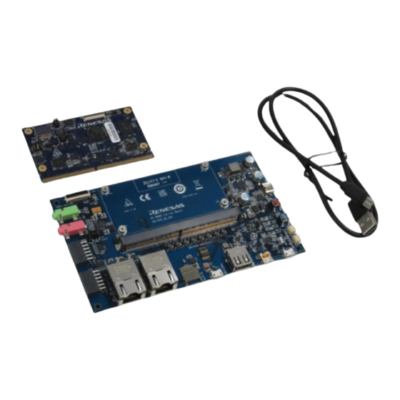
RZ Family / RZ/G, RZ/A Series 5. Appendix Appendix Type Name and Features of Each Board This section describes the the type name and feature of each board here. The SMARC Module Board is as follows. This picture is of the RTK9743U11C01000BE. Figure 5.1 Top View of the SMARC Module Board The SMARC Module Boards with RZ/G2UL, RZ/A3UL and RZ/Five are used common PCB layout and designed to be... - Page 76 RZ Family / RZ/G, RZ/A Series 5. Appendix The RZ SMARC Series Carrier Board is as follows. This picture is of the RTK97X4XXXB00000BE. Figure 5.2 Top View of the RZ SMARC Series Carrier Board Board Name Type Name RZ SMARC Series Carrier Board RTK97X4XXXB00000BE The Evaluation board Kit is as follows.
- Page 77 RZ Family / RZ/G, RZ/A Series 5. Appendix The Evaluation board Kits are similarly designed to use a common board layout and to be pin-compatible. Parallel to HDMI Board Name Type Name Memory Configuration Conversion Board Evaluation board Kit for RZ/G2UL RTK9743U11S01000BE RZ/G2UL QSPI flash memory Included...
-
Page 78: How To Identify Each Smarc Module Board
RZ Family / RZ/G, RZ/A Series 5. Appendix How to Identify Each SMARC Module Board The differences between each SMARC Module Board are as follows. This picture is of the RTK9743U11C01000BE. Table 5.1 Comparison of the RTK9743U11C01000BE and the RTK9743F01C01000BE Type Name RTK9743U11C01000BE RTK9743F01C01000BE... -
Page 79: How To Replace The Smarc Module Board
RZ Family / RZ/G, RZ/A Series 5. Appendix How to replace the SMARC Module Board Please be careful when replacing the board as follows. Remove the four screws. NOTE The screw thread is a special shape, so be careful not to crush the screw thread. Please recommend to prepare a torx screwdriver which is a “T6”... - Page 80 RZ Family / RZ/G, RZ/A Series 5. Appendix Insert the replacement the SMARC Module Board diagonally, then roll the board parallel to the RZ SMARC Series Carrier Board and fix it with screws. Figure 5.7 How to install the SMARC Module Board R01UH0990EJ0101 Rev.1.01 Page 80 of 83...
-
Page 81: Revision History
RZ Family / RZ/G, RZ/A Series REVISION HISTORY RZ Family / RZ/G, RZ/A Series REVISION HISTORY RZ/G2UL, RZ/A3UL, RZ/Five SMARC Module Board REVISION HISTORY Description Rev. Date Page Summary ⎯ 1.00 Jun 27, 2022 First edition issued 1.01 Jul 28, 2022 9, 15 The section title is changed from "RT9743U11C01000BE"... - Page 82 Colophon RZ/G2UL, RZ/A3UL, RZ/Five SMARC Module Board User’s Manual: Hardware Publication Date: Rev.1.01 Jul 28, 2022 Rev.1.00 Jun 27, 2022 Published by: Renesas Electronics Corporation...
- Page 83 Back Cover RZ Family / RZ/G, RZ/A Series R01UH0990EJ0101...
Need help?
Do you have a question about the RZ Series and is the answer not in the manual?
Questions and answers