Table of Contents
Advertisement
Quick Links
AP0101AT2L00XPGAH3-GEVB
AP0101AT Evaluation Board
User's Manual
Evaluation Board Overview
The evaluation boards are designed to demonstrate the features of
ON Semiconductor's image sensors products. This headboard is
intended to plug directly into the Demo 3 system. Test points and
jumpers on the board provide access to the clock, I/Os, and other
miscellaneous signals.
Features
•
Clock Input
Default – 27 MHz Crystal Oscillator
♦
Optional Demo 3 Controlled MClk
♦
•
Two Wire Serial Interface
•
Parallel Interface
•
HiSPi (High Speed Serial Pixel) Interface
•
ROHS Compliant
Block Diagram
© Semiconductor Components Industries, LLC, 2015
October, 2015 − Rev. 0
Arrow.com.
Downloaded from
Figure 2. Block Diagram of AP0101AT2L00XPGAH3−GEVB
www.onsemi.com
EVAL BOARD USER'S MANUAL
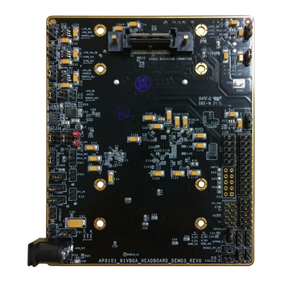
Figure 1. AP0101AT Evaluation Board
1
Publication Order Number:
EVBUM2322/D
Advertisement
Table of Contents

Related Manuals for ON Semiconductor AP0101AT


Summary of Contents for ON Semiconductor AP0101AT
- Page 1 Evaluation Board Overview The evaluation boards are designed to demonstrate the features of www.onsemi.com ON Semiconductor’s image sensors products. This headboard is intended to plug directly into the Demo 3 system. Test points and EVAL BOARD USER’S MANUAL jumpers on the board provide access to the clock, I/Os, and other miscellaneous signals.
- Page 2 AP0101AT2L00XPGAH3−GEVB Top View +1V2_VCCINT P17 +AVDD P13 Baseboard Connector J1 +VCC P18 +HVCCIO P22 +HVDDIO P15 +VCCIO P16 SHUTDOWN P25 OSC/XTAL Sel P19 MCLK_IN P26 SEN_SDATA P33, P34 CLK_SELECT P23 TRST_N P8 STANDBY P7 SADDR P5 SPI_BUS P38 SPI Memory Selection P11 BGLE_SCL_ISP P1 SPI_SDI P10, P12 BGLE_SDA_ISP P3...
- Page 3 AP0101AT2L00XPGAH3−GEVB Jumper Pin Locations The jumpers on headboards start with Pin 1 on the leftmost side of the pin. Grouped jumpers increase in pin size with each jumper added. Pin 1 Pins 1−4 Figure 5. Pin Locations for a Single Jumper. Pin 1 is Located at the Leftmost Side and Increases as it Moves to the Right Pin 1 Pins 1 and 2...
- Page 4 AP0101AT2L00XPGAH3−GEVB Table 1. JUMPERS AND HEADERS (continued) Jumper/Header No. Jumper/Header Name Pins Description +AVDD 1−2(Default) Adjusts On-Board Regulator to +1.8 V, Internal Regulator use 2−3 +1.8 V Supply from Demo 3 +HVDDIO 1−2(Default) Connects to On-Board +HVDDIO Power Supply 2−3 External Power Supply Connection +VCCIO 1−2(Default)
- Page 5 AP0101AT2L00XPGAH3−GEVB Interfacing to ON Semiconductor Demo 3 Baseboard The ON Semiconductor Demo 3 headboard has a similar 52-pin connector which mates with J1 of the adapter board. 52-pin connector which mates with P6 of the adapter board. The four mounting holes secure the baseboard and the The ON Semiconductor Demo 3 baseboard has a similar headboard with spacers and screws.
- Page 6 onsemi, , and other names, marks, and brands are registered and/or common law trademarks of Semiconductor Components Industries, LLC dba “onsemi” or its affiliates and/or subsidiaries in the United States and/or other countries. onsemi owns the rights to a number of patents, trademarks, copyrights, trade secrets, and other intellectual property. A listing of onsemi’s product/patent coverage may be accessed at www.onsemi.com/site/pdf/Patent−Marking.pdf.
Need help?
Do you have a question about the AP0101AT and is the answer not in the manual?
Questions and answers