Table of Contents
Advertisement
Quick Links
AP0100CSSL00SPGAH-GEVB
AP0100CS Evaluation Board
User's Manual
Evaluation Board Overview
The evaluation boards are designed to demonstrate the features of
ON Semiconductor's image sensors products. This headboard is
intended to plug directly into the Demo 2X system. Test points and
jumpers on the board provide access to the clock, I/Os, and other
miscellaneous signals.
Features
•
Clock Input
Default – 27 MHz Crystal Oscillator
♦
Optional Demo 2X Controlled MClk
♦
•
Two Wire Serial Interface
•
Parallel Interface
•
HiSPi (High Speed Serial Pixel) Interface
•
ROHS Compliant
Block Diagram
© Semiconductor Components Industries, LLC, 2015
September, 2015 − Rev. 0
Figure 2. Block Diagram of AP0100CSSL00SPGAH−GEVB
EVAL BOARD USER'S MANUAL
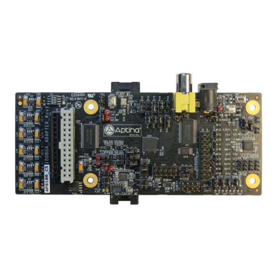
Figure 1. AP0100CS Evaluation Board
1
www.onsemi.com
Publication Order Number:
EVBUM2316/D
Advertisement
Table of Contents

Related Manuals for ON Semiconductor AP0100CS


Summary of Contents for ON Semiconductor AP0100CS
- Page 1 Evaluation Board Overview The evaluation boards are designed to demonstrate the features of www.onsemi.com ON Semiconductor’s image sensors products. This headboard is intended to plug directly into the Demo 2X system. Test points and EVAL BOARD USER’S MANUAL jumpers on the board provide access to the clock, I/Os, and other miscellaneous signals.
- Page 2 AP0100CSSL00SPGAH−GEVB Top View Headboard Connector J8 Headboard Connector J7 1OE/2OE P54 SEN_CLK P30 SEN_RST_OUT P51 EEPROM Sel P47, P48, P59 SEN_DATA P31 MCLK_IN P16 OSC/XTAL Sel P22, P23 SPI_SDI_BAR P5 VDD P26 SPI_SCLK/CS_N P44 Video Filter Sel P56, P57, P58 SPI Mem.
- Page 3 AP0100CSSL00SPGAH−GEVB Jumper Pin Locations The jumpers on headboards start with Pin 1 on the leftmost side of the pin. Grouped jumpers increase in pin size with each jumper added. Pin 1 Pins 1−4 Figure 5. Pin Locations for a Single Jumper. Pin 1 is Located at the Leftmost Side and Increases as it Moves to the Right Pin 1 Pins 1 and 2...
- Page 4 AP0100CSSL00SPGAH−GEVB Table 1. JUMPERS AND HEADERS (continued) Jumper/Header No. Jumper/Header Name Pins Description ON_LED 1−2 (Default) Connects to On-Board to Indicate Power On +HVDDIO 1−2 (Default) Connects to On-Board +HVDDIO Power Supply 2−3 External Power Supply Connection +VCC 1−2 (Default) Connects to On-Board +VCC Power Supply 2−3 External Power Supply Connection...
- Page 5 AP0100CSSL00SPGAH−GEVB Table 1. JUMPERS AND HEADERS (continued) Jumper/Header No. Jumper/Header Name Pins Description P38, P39 IO Expander U38 P39 Open, EEPROM Address Set to 0x48 Setting P38 Closed (Default) P39 Open, EEPROM Address Set to 0x4C P38 Open P39 Closed, EEPROM Address Set to 0x44 P38 Open P39 Closed,...
- Page 6 AP0100CSSL00SPGAH−GEVB Interfacing to ON Semiconductor Demo 2X Baseboard The ON Semiconductor 2X baseboard has a similar and J6 of the headboard. The four mounting holes secure the 26-pin connector and 13-pin connector which mate with J5 baseboard and the headboard with spacers and screws.
- Page 7 onsemi, , and other names, marks, and brands are registered and/or common law trademarks of Semiconductor Components Industries, LLC dba “onsemi” or its affiliates and/or subsidiaries in the United States and/or other countries. onsemi owns the rights to a number of patents, trademarks, copyrights, trade secrets, and other intellectual property. A listing of onsemi’s product/patent coverage may be accessed at www.onsemi.com/site/pdf/Patent−Marking.pdf.
Need help?
Do you have a question about the AP0100CS and is the answer not in the manual?
Questions and answers