Table of Contents
Advertisement
Quick Links
AP0200ATSL00XEGAH3-GEVB
AP0200AT Evaluation Board
User's Manual
Evaluation Board Overview
The evaluation boards are designed to demonstrate the features of
ON Semiconductor's image sensors products. This headboard is
intended to plug directly into the Demo 3 system. Test points and
jumpers on the board provide access to the clock, I/Os, and other
miscellaneous signals.
Features
•
Clock Input
Default – 27 MHz Crystal Oscillator
♦
Optional Demo 3 Controlled MClk
♦
•
Two Wire Serial Interface
Selectable Base Address
♦
•
Parallel Interface
•
HiSPi (High Speed Serial Pixel) Interface
•
ROHS Compliant
Block Diagram
© Semiconductor Components Industries, LLC, 2015
September, 2015 − Rev. 0
Arrow.com.
Downloaded from
Figure 2. Block Diagram of AP0200ATSL00XEGAH3−GEVB
www.onsemi.com
EVAL BOARD USER'S MANUAL
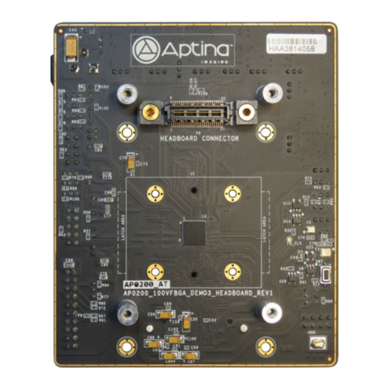
Figure 1. AP0200AT Evaluation Board
1
Publication Order Number:
EVBUM2319/D
Advertisement
Table of Contents

Related Manuals for ON Semiconductor AP0200ATSL00XEGAH3-GEVB


Summary of Contents for ON Semiconductor AP0200ATSL00XEGAH3-GEVB
- Page 1 Evaluation Board Overview The evaluation boards are designed to demonstrate the features of www.onsemi.com ON Semiconductor’s image sensors products. This headboard is intended to plug directly into the Demo 3 system. Test points and EVAL BOARD USER’S MANUAL jumpers on the board provide access to the clock, I/Os, and other miscellaneous signals.
- Page 2 AP0200ATSL00XEGAH3−GEVB Top View Headboard Connector P6 RESET Switch SW7 Figure 3. Top View of the Board − Default Jumpers Bottom View +VDDIO P21 +VDDIO Select P57 +2V8_VAA_OTPM P14 +VDDIO_LS P13 ON_LED P11 +VDDIO_SENSOR P19 +5V0 P8 +2V8_VDDPHY P12 +1V8_VAA P41 SEN_DATA P51 +3V3 P24 TRIGGER P59...
- Page 3 AP0200ATSL00XEGAH3−GEVB Jumper Pin Locations The jumpers on headboards start with Pin 1 on the leftmost side of the pin. Grouped jumpers increase in pin size with each jumper added. Pin 1 Pins 1−4 Figure 5. Pin Locations for a Single Jumper. Pin 1 is Located at the Leftmost Side and Increases as it Moves to the Right Pin 1 Pins 1 and 2...
- Page 4 AP0200ATSL00XEGAH3−GEVB Table 1. JUMPERS AND HEADERS (continued) Jumper/Header No. Jumper/Header Name Pins Description +VDDIO 2−3 (Default) Using On-Board Power Supply 1−2 Using +1V8_HB or +2V8_HB Power Supply from Demo 3 Baseboard P22, P23 OSC/XTAL Select P22 2−3, Oscillator/Demo Clock Selected P23 Open (Default) P22 1−2, On-Board Crystal Selected...
- Page 5 When Pushed, 240 ms Reset Signal will be Sent to AP0200 Interfacing to ON Semiconductor Demo 3 Baseboard The ON Semiconductor Demo 3 baseboard has a similar The four mounting holes secure the baseboard and the 52-pin connector which mates with J1 of the headboard.
- Page 6 onsemi, , and other names, marks, and brands are registered and/or common law trademarks of Semiconductor Components Industries, LLC dba “onsemi” or its affiliates and/or subsidiaries in the United States and/or other countries. onsemi owns the rights to a number of patents, trademarks, copyrights, trade secrets, and other intellectual property. A listing of onsemi’s product/patent coverage may be accessed at www.onsemi.com/site/pdf/Patent−Marking.pdf.
Need help?
Do you have a question about the AP0200ATSL00XEGAH3-GEVB and is the answer not in the manual?
Questions and answers