Advertisement
Quick Links
ARX3A0 - CSP35
ARX3A0 - CSP35 Evaluation
Board User's Manual
Evaluation Board Overview
The evaluation boards are designed to demonstrate the features of
ON Semiconductor's image sensors products. This headboard is
intended to plug directly into the Demo3 system. Test points and
jumpers on the board provide access to the clock, I/Os and other
miscellaneous signals.
Features
•
Clock Input
♦
Default − 27 MHz Crystal Oscillator
♦
Optional Demo3 Controlled MClk
•
Two Wire Serial Interface
♦
Selectable Base Address
•
2 Lane MIPI Interface
•
RoHS Compliant
Block Diagram
© Semiconductor Components Industries, LLC, 2020
November, 2020 − Rev. 0
Figure 2. Block Diagram of ARX3A0 Evaluation Board
EVAL BOARD USER'S MANUAL
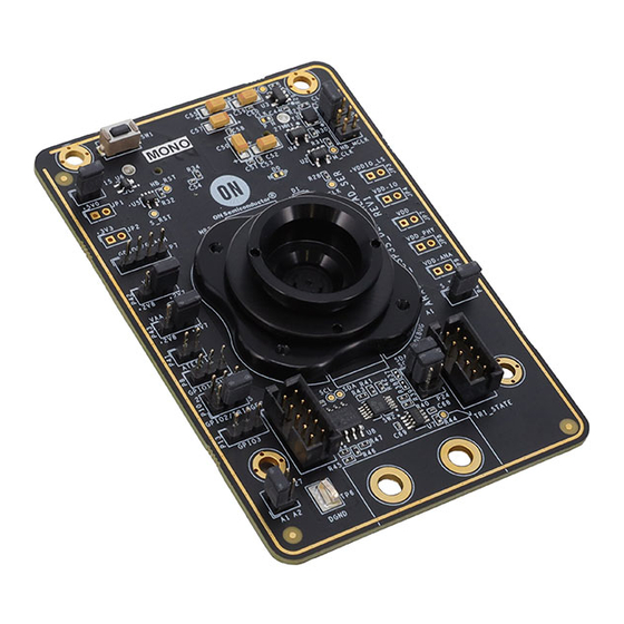
Figure 1. ARX3A0 Evaluation Board
1
www.onsemi.com
Publication Order Number:
EVBUM2783/D
Advertisement

Subscribe to Our Youtube Channel
Related Manuals for ON Semiconductor ARX3A0-CSP35


Summary of Contents for ON Semiconductor ARX3A0-CSP35
- Page 1 The evaluation boards are designed to demonstrate the features of EVAL BOARD USER’S MANUAL ON Semiconductor’s image sensors products. This headboard is intended to plug directly into the Demo3 system. Test points and jumpers on the board provide access to the clock, I/Os and other miscellaneous signals.
- Page 2 ARX3A0 − CSP35 Top View SWITCH SW1 LED P15 CLK Sel P20 GPIO 0/FLASH P7 VAA SEL P42 VAA_PIX SEL P43 A TEST P4 1 GPIO1/SHUTTER TEST P40 GPIO2/TRIGGER GPIO3 P13 MASTER HEADER P26 SLAVE HEADER P25 I2C P24 EEPROM ADDR SEL P27 Figure 3.
- Page 3 ARX3A0 − CSP35 Jumper Locations The jumpers on headboards start with Pin 1 on the leftmost side of the pin. Grouped jumpers increase in pin size with each jumper added. Pin 1 Pins 1 − 4 Figure 5. Pin Locations for a Single Jumper. Pin 1 is Located at the Leftmost Side and Increases as it Moves to the Right Pin 1 Figure 6.
- Page 4 ARX3A0 − CSP35 Jumper/Header Functions & Default Positions Table 1. JUMPERS AND HEADERS Jumper/Header No. Jumper/Header Name Pins Description GPIO0/FLASH Open (Default) +5V0 GPIO0/FLASH +3V3 SHUTTER / GPIO1 Open (Default) Normal Operation 1−2 Pulled Up 2−3 Pulled low GPIO2/TRIGGER 3−5 (Default) GPIO2 Pull Down 1−3 GPIO2 Pull Up...
- Page 5 ARX3A0 − CSP35 Interfacing to ON Semiconductor Demo3 Baseboard Table 2. SHORTED JUMPERS FOR POWER The ON Semiconductor Demo3 baseboard has a similar MEASUREMENT 52−pin connector P5 which mates with J1 of the headboard. Jumper Voltage (V) The four mounting holes secure the baseboard and the JP1 (From Demo3) headboard with spacers and screws.
-
Page 6: Technical Support
LIMITATIONS OF LIABILITY: ON Semiconductor shall not be liable for any special, consequential, incidental, indirect or punitive damages, including, but not limited to the costs of requalification, delay, loss of profits or goodwill, arising out of or in connection with the board, even if ON Semiconductor is advised of the possibility of such damages. In no event shall ON Semiconductor’s aggregate liability from any obligation arising out of or in connection with the board, under any theory of liability, exceed the purchase price paid for the board, if any.
Need help?
Do you have a question about the ARX3A0-CSP35 and is the answer not in the manual?
Questions and answers