Table of Contents

Related Manuals for Texas Instruments LMK04816


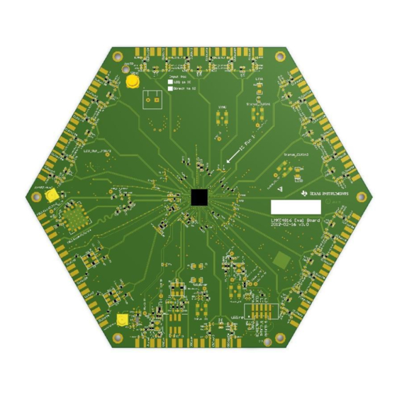
Summary of Contents for Texas Instruments LMK04816
- Page 1 O P E R A T I N G I N S T R U C T I O N S LMK04816 Low-Noise Clock Jitter Cleaner with Dual Loop PLLs LMK04816 Evaluation Board Operating Instructions Texas Instruments June 2012 SNLU107...
-
Page 2: Table Of Contents
........................... 4 VAILABLE AMILY EVICES QUICK START ................................. 5 ....................6 EFAULT OADER ODES FOR VALUATION OARDS EXAMPLE: USING CODELOADER TO PROGRAM THE LMK04816 ................7 1. S ..........................7 TART OADER PPLICATION 2. S ................................7 ELECT EVICE 3. P ............................. - Page 3 L M K 0 4 8 1 6 E V A L U A T I O N B O A R D O P E R A T I N G I N S T R U C T I O N S LMK04816B CLKout Phase Noise ........................
-
Page 4: General Description
(1) CodeLoader uWire cable (LPT uWire) Available LMK04816 Evaluation Boards The LMK04816 Evaluation Board supports any of the four devices offered in the LMK04816 Family. A commercial-quality VCXO is also mounted to the board to provide a known reference point for evaluating device performance and functionality. -
Page 5: Quick Start
Power 5.0 V 5.0 V 3.3 V (LDO) Factory default is LDO is used. Customer may reconfigure to power LMK directly. LMK04816 uWire header Reference clock from signal generator or other external source. Program with CodeLoader 122.88 MHz Be sure to press ‘Ctrl - L’... -
Page 6: Default Codeloader Modes For Evaluation Boards
PLL2 Crystal Oscillator 122.88 MHz 20.48 MHz VCXO Enabled The next section outlines step-by-step procedures for using the evaluation board with the LMK04816. For boards with another part number, make sure to select the corresponding part number under the “Device” menu. SNLU107... -
Page 7: Example: Using Codeloader To Program The Lmk04816
The purpose of this section is to walk the user through using CodeLoader 4 to make some measurements with the LMK04816 device as an example. For more information on CodeLoader refer to Appendix A: CodeLoader Usage or the CodeLoader 4 instructions located at http://www.ti.com/tool/codeloader/. -
Page 8: Program/Load Device
Troubleshooting Information contains information on troubleshooting communications. 4. Restoring a Default Mode Click “Mode” “LMK04816, 122.88 MHz VCXO, 122.88 MHz CLKin1”; then press Ctrl+L. Figure 5: Setting the Default mode for LMK04816 For the purpose of this walkthrough, a default mode will be loaded to ensure a common starting point. -
Page 9: Visual Confirmation Of Frequency Lock
L M K 0 4 8 1 6 E V A L U A T I O N B O A R D O P E R A T I N G I N S T R U C T I O N S 5. - Page 10 L M K 0 4 8 1 6 E V A L U A T I O N B O A R D O P E R A T I N G I N S T R U C T I O N S Norm/Inv or Inv/Norm.
-
Page 11: Pll Loop Filters And Loop Parameters
The loop filters on the LMK04816 evaluation board are setup using the approach above. The loop filter for PLL1 has been configured for a narrow loop bandwidth (< 100 Hz), while the loop filter of PLL2 has been configured for a wide loop bandwidth (>... -
Page 12: Pll2 Loop Filter
L M K 0 4 8 1 6 E V A L U A T I O N B O A R D O P E R A T I N G I N S T R U C T I O N S PLL2 Loop Filter Table 5: PLL2 Loop Filter Parameters for LMK04816B LMK04816B... -
Page 13: Evaluation Board Inputs And Outputs
Unless otherwise noted, the connectors described can be assumed to be populated by default. Additionally, some applicable CodeLoader programming controls are noted for convenience. Refer to the LMK04816 Family Datasheet for complete register programming information. Table 6: Evaluation Board Inputs and Outputs... - Page 14 L M K 0 4 8 1 6 E V A L U A T I O N B O A R D O P E R A T I N G I N S T R U C T I O N S Signal Type, Connector Name Description...
- Page 15 L M K 0 4 8 1 6 E V A L U A T I O N B O A R D O P E R A T I N G I N S T R U C T I O N S Signal Type, Connector Name Description...
- Page 16 CLKin1* is the default reference clock input selected in CodeLoader. The clock input selection mode can be programmed on the Bits/Pins tab via the CLKin_Select_MODE control. Refer to the LMK04816 Family Datasheet section “Input Clock Populated: Switching” for more information. CLKin0, CLKin0*,...
- Page 17 OSCin/OSCin* pins and must be AC coupled. If operated in single-ended mode, the unused input must be connected to GND with 0.1 uF. Refer to the LMK04816 Family Datasheet section “Electrical Characteristics” for PLL2 Reference Input (OSCin) specifications.
- Page 18 Not populated: Output selected on the Bits/Pins tab via the LD_MUX control. Status_LD Refer to the LMK04816 Family Datasheet section “Status Pins” and “Digital Lock Detect” for more information. Note: Before a high-frequency internal signal (e.g. PLL divider output signal) is selected by LD_MUX, it is suggested to first remove the 270 ohm resistor to prevent the LED from loading the output.
- Page 19 Status_CLKin1 Status_CLKin0 Clock CLKin0 CLKin1 Reserved Refer to the LMK04816 Family Datasheet section “Input Clock Switching” for more information. Status Outputs When Status_CLKinX_TYPE is 3 to 6 (pin enabled as an output), the status output signal for the corresponding Status_CLKinX pin can be programmed on the Bits/Pins tab via the Status_CLKinX_MUX control.
- Page 20 A SYNC event can also be programmed by toggling the SYNC_POL_INV bit in the Bits/Pins tab in CodeLoader. Refer to the LMK04816 Family Datasheet section “Clock Output Synchronization” for more information. Status Output When SYNC_MUX is 3 to 6 (pin enabled as output), a status signal for the SYNC pin can be selected on the Bits/Pins tab via the SYNC_MUX control.
-
Page 21: Recommended Test Equipment
L M K 0 4 8 1 6 E V A L U A T I O N B O A R D O P E R A T I N G I N S T R U C T I O N S Recommended Test Equipment Power Supply The Power Supply should be a low noise power supply, particularly when the devices on the... -
Page 22: Programming 0-Delay Mode In Codeloader
(VCO) frequency of the PLL1 tab to the frequency of the fed back output clock will re-program the PLL1 N divider to allow the LMK04816 will be able to lock. The PLL1 loop has been altered and actual VCXO no longer directly feeds into PLL1 N divider. The VCXO is only used... - Page 23 It is up to the user to ensure the PLL dividers are programmed correctly. To illustrate the proper programming of the LMK04816 device in dual loop 0-delay mode the following case examples are provided. Note that in one of the cases, the feedback frequency from the clock output matches the VCXO frequency and CodeLoader will display the proper frequency values.
-
Page 24: Single Loop 0-Delay Mode Examples
This permits phase alignment between the clock output and the OSCin input (0-Delay). As such, the PLL2_N, PLL2_R, and PLL2_N_CAL divide values may need to be adjusted to permit the LMK04816 to lock. Programming Steps 1. Program the Single Loop 0-Delay mode. - Page 25 L M K 0 4 8 1 6 E V A L U A T I O N B O A R D O P E R A T I N G I N S T R U C T I O N S Case 4 shows 0-Delay mode with CLKout divider not equal to the PLL2_P value;...
-
Page 26: Appendix A: Codeloader Usage
L M K 0 4 8 1 6 E V A L U A T I O N B O A R D O P E R A T I N G I N S T R U C T I O N S Appendix A: CodeLoader Usage Code Loader is used to program the evaluation board with either an LPT port using the included CodeLoader cable or with a USB port using the optional USB-to-uWire cable available from... -
Page 27: Clock Outputs Tab
L M K 0 4 8 1 6 E V A L U A T I O N B O A R D O P E R A T I N G I N S T R U C T I O N S Clock Outputs Tab Figure 9: Clock Outputs tab The Clock Outputs tab allows the user to control the output channel blocks, including:... - Page 28 L M K 0 4 8 1 6 E V A L U A T I O N B O A R D O P E R A T I N G I N S T R U C T I O N S Clicking on the cyan-colored PLL2 block that contains R, PDF and N values will bring the PLL2 tab into focus where these values may be modified, if needed.
-
Page 29: Pll1 Tab
L M K 0 4 8 1 6 E V A L U A T I O N B O A R D O P E R A T I N G I N S T R U C T I O N S PLL1 Tab Figure 11: PLL1 tab The PLL1 tab allows the user to change the following parameters in Table 8. -
Page 30: Setting The Pll1 Vco Frequency And Pll2 Reference Frequency
L M K 0 4 8 1 6 E V A L U A T I O N B O A R D O P E R A T I N G I N S T R U C T I O N S N Counter PLL1_N PLL1 N Counter value (1 to 16383). -
Page 31: Pll2 Tab
L M K 0 4 8 1 6 E V A L U A T I O N B O A R D O P E R A T I N G I N S T R U C T I O N S PLL2 Tab Figure 12: PLL2 tab The PLL2 tab allows the user to change the following parameters in Table 9. -
Page 32: Bits/Pins Tab
Brief descriptions for the controls on this tab are provided in Table 10 to supplement the datasheet. Refer to the LMK04816 Family Datasheet for more information. TIP: Right-clicking any register name in the Bits/Pins tab will display a Help prompt with the register address, data bit location/length, and a brief register description. - Page 33 R0 is programmed. POWERDOWN Places the device in powerdown mode. MODE Selects the operating mode (topology) for the LMK04816 device. PD_OSCin Powers down the OSCin buffer. For use in Clock Distribution mode if OSCin path is not used. FEEDBACK_MUX Selects the feedback source for 0-delay mode.
- Page 34 L M K 0 4 8 1 6 E V A L U A T I O N B O A R D O P E R A T I N G I N S T R U C T I O N S HOLDOVER_TYPE Sets I/O pin type on the Status_Holdover pin.
- Page 35 L M K 0 4 8 1 6 E V A L U A T I O N B O A R D O P E R A T I N G I N S T R U C T I O N S HOLD_DLD_CNT In HOLDOVER mode, wait for this many clocks of PLL1 PDF within the tolerances of PLL1_WND...
- Page 36 L M K 0 4 8 1 6 E V A L U A T I O N B O A R D O P E R A T I N G I N S T R U C T I O N S PLL1_R_DLY R delay causes clock outputs to lag clock input when in a 0-delay mode.
-
Page 37: Registers Tab
L M K 0 4 8 1 6 E V A L U A T I O N B O A R D O P E R A T I N G I N S T R U C T I O N S Registers Tab Figure 14: Registers Tab The Registers tab shows the value of each register. -
Page 38: Appendix B: Typical Phase Noise Performance Plots
L M K 0 4 8 1 6 E V A L U A T I O N B O A R D O P E R A T I N G I N S T R U C T I O N S Appendix B: Typical Phase Noise Performance Plots PLL1 The LMK04816B‟s dual PLL architecture achieves ultra low jitter and phase noise by allowing... -
Page 39: Clock Output Measurement Technique
L M K 0 4 8 1 6 E V A L U A T I O N B O A R D O P E R A T I N G I N S T R U C T I O N S VCXO Phase Noise CVHD-950-122.88 -100... -
Page 40: Clock Outputs (Clkout)
I N S T R U C T I O N S Clock Outputs (CLKout) The LMK04816 Family features programmable LVDS, LVPECL, and LVCMOS buffer modes for the CLKoutX and OSCout0 output pairs. Included below are various phase noise measurements for each output format. -
Page 41: Lmk04816B Oscout Phase Noise
L M K 0 4 8 1 6 E V A L U A T I O N B O A R D O P E R A T I N G I N S T R U C T I O N S For the LMK04816B, the internal VCO frequency is 2457.60 MHz. - Page 42 L M K 0 4 8 1 6 E V A L U A T I O N B O A R D O P E R A T I N G I N S T R U C T I O N S Table 16: LMK04816B OSCout Phase Noise and RMS Jitter (fs) OSCout0 OSCin thru...
-
Page 43: Appendix C: Schematics
Designed for: Evaluation Customer Mod. Date: 4/26/2012 Texas Instruments and/or its licensors do not warrant the accuracy or completeness of this LP5900 Component values Project: LMK04816 Evaluation Board specification or any information contained therein. Texas Instruments and/or its licensors do not C359 = 0.47 uF... -
Page 44: Lmk04816B Device With Loop Filter And Crystal Circuits
Designed for: Evaluation Customer Mod. Date: 4/26/2012 Texas Instruments and/or its licensors do not warrant the accuracy or completeness of this Project: LMK04816 Evaluation Board specification or any information contained therein. Texas Instruments and/or its licensors do not Sheet Title:... -
Page 45: Reference Inputs (Clkin0, Clkin1, & Clkin2), External Vcxo (Oscin) & Vco Circuits
Designed for: Evaluation Customer Mod. Date: 4/26/2012 Texas Instruments and/or its licensors do not warrant the accuracy or completeness of this Project: LMK04816 Evaluation Board specification or any information contained therein. Texas Instruments and/or its licensors do not Sheet Title:... -
Page 46: Clock Outputs (Osc Out 0, Clk Out To Clk Out 3)
Designed for: Evaluation Customer Mod. Date: 4/26/2012 Texas Instruments and/or its licensors do not warrant the accuracy or completeness of this Project: LMK04816 Evaluation Board 1. Designators greater than and equal to 300 are placed on bottom of PCB specification or any information contained therein. Texas Instruments and/or its licensors do not... -
Page 47: Clock Outputs (Clkout4 To Clkout7)
Designed for: Evaluation Customer Mod. Date: 4/26/2012 Texas Instruments and/or its licensors do not warrant the accuracy or completeness of this Project: LMK04816 Evaluation Board specification or any information contained therein. Texas Instruments and/or its licensors do not Sheet Title:... -
Page 48: Clock Outputs (Clkout8 To Clkout11)
Designed for: Evaluation Customer Mod. Date: 4/26/2012 Texas Instruments and/or its licensors do not warrant the accuracy or completeness of this Project: LMK04816 Evaluation Board specification or any information contained therein. Texas Instruments and/or its licensors do not Sheet Title:... -
Page 49: Uwire Header, Logic I/O Ports And Status Leds
Designed for: Evaluation Customer Mod. Date: 4/26/2012 Texas Instruments and/or its licensors do not warrant the accuracy or completeness of this Project: LMK04816 Evaluation Board specification or any information contained therein. Texas Instruments and/or its licensors do not Sheet Title:... -
Page 50: Usb Interface
Designed for: Evaluation Customer Mod. Date: 4/26/2012 Texas Instruments and/or its licensors do not warrant the accuracy or completeness of this Project: LMK04816 Evaluation Board specification or any information contained therein. Texas Instruments and/or its licensors do not Sheet Title: USB Control. -
Page 51: Appendix D: Bill Of Materials
B O A R D O P E R A T I N G I N S T R U C T I O N S Appendix D: Bill of Materials Table 17: Bill of Materials for LMK04816 Evaluation Boards Item Designator Description... - Page 52 L M K 0 4 8 1 6 E V A L U A T I O N B O A R D O P E R A T I N G I N S T R U C T I O N S C2, C12, C41, CAP, CERM, 0.1uF, 16V, +/-10%, X7R, 0603 Kemet...
- Page 53 L M K 0 4 8 1 6 E V A L U A T I O N B O A R D O P E R A T I N G I N S T R U C T I O N S Cb1_B1 CAP, CERM, 0.33uF, 16V, +/-10%, X7R, 0603 Kemet...
- Page 54 CRCW060347K0JNEA Rb2_B1 RES, 3.9k ohm, 5%, 0.1W, 0603 Vishay-Dale CRCW06033K90JNEA S1, S2, S3, S4, S5, 0.875" Standoff VOLTREX SPCS-14 LMK04816 Texas Instruments LMK04816BISQ 122.88 MHz VCXO Crystek CVHD-950-122.88 U4, U300 Precison Single Low Noise, Low 1/F corner Op Amp National...
- Page 55 L M K 0 4 8 1 6 E V A L U A T I O N B O A R D O P E R A T I N G I N S T R U C T I O N S Semiconductor U302 Micropower 800mA Low Noise 'Ceramic Stable'...
-
Page 56: Appendix E: Pcb Layers Stackup
L M K 0 4 8 1 6 E V A L U A T I O N B O A R D O P E R A T I N G I N S T R U C T I O N S Appendix E: PCB Layers Stackup 6-layer PCB Stackup includes: Top Layer for high-priority high-frequency signals (2 oz.) -
Page 57: Appendix F: Pcb Layout
L M K 0 4 8 1 6 E V A L U A T I O N B O A R D O P E R A T I N G I N S T R U C T I O N S Appendix F: PCB Layout Layer #1 –... -
Page 58: Layer #2 - Rf Ground Plane (Inverted)
L M K 0 4 8 1 6 E V A L U A T I O N B O A R D O P E R A T I N G I N S T R U C T I O N S Layer #2 –... -
Page 59: Layer #3 - Vcc Planes
L M K 0 4 8 1 6 E V A L U A T I O N B O A R D O P E R A T I N G I N S T R U C T I O N S Layer #3 –... -
Page 60: Layer #4 - Ground Plane (Inverted)
L M K 0 4 8 1 6 E V A L U A T I O N B O A R D O P E R A T I N G I N S T R U C T I O N S Layer #4 –... -
Page 61: Layer # 5 - Vcc Planes 2
L M K 0 4 8 1 6 E V A L U A T I O N B O A R D O P E R A T I N G I N S T R U C T I O N S Layer # 5 –... -
Page 62: Layer #6 - Bottom
L M K 0 4 8 1 6 E V A L U A T I O N B O A R D O P E R A T I N G I N S T R U C T I O N S Layer #6 –... -
Page 63: Layers #1 And 6 - Top And Bottom (Composite)
L M K 0 4 8 1 6 E V A L U A T I O N B O A R D O P E R A T I N G I N S T R U C T I O N S Layers #1 and 6 –... - Page 64 L M K 0 4 8 1 6 E V A L U A T I O N B O A R D O P E R A T I N G I N S T R U C T I O N S SNLU107...
-
Page 65: Appendix G: Properly Configuring Lpt Port
L M K 0 4 8 1 6 E V A L U A T I O N B O A R D O P E R A T I N G I N S T R U C T I O N S Appendix G: Properly Configuring LPT Port When trying to solve any communications issue, it is most convenient to verify communication by programming the POWERDOWN bit to confirm normal or low supply current consumption... -
Page 66: Correct Lpt Mode
L M K 0 4 8 1 6 E V A L U A T I O N B O A R D O P E R A T I N G I N S T R U C T I O N S Figure 19: Selecting the LPT Port Address Correct LPT Mode If communications are not working, then it is possible the LPT port mode is set improperly. -
Page 67: Appendix H: Troubleshooting Information
L M K 0 4 8 1 6 E V A L U A T I O N B O A R D O P E R A T I N G I N S T R U C T I O N S Appendix H: Troubleshooting Information If the evaluation board is not behaving as expected, the most likely issues are…... -
Page 68: Confirm Pll2 Operation/Locking
L M K 0 4 8 1 6 E V A L U A T I O N B O A R D O P E R A T I N G I N S T R U C T I O N S 3) Confirm PLL2 operation/locking 1) Program LD_MUX = “PLL2_R/2”... - Page 69 I N S T R U C T I O N S EVALUATION BOARD/KIT/MODULE (EVM) ADDITIONAL TERMS Texas Instruments (TI) provides the enclosed Evaluation Board/Kit/Module (EVM) under the following conditions: The user assumes all responsibility and liability for proper and safe handling of the goods. Further, the user indemnifies TI from all claims arising from the handling or use of the goods.
- Page 70 O P E R A T I N G I N S T R U C T I O N S is strictly prohibited and unauthorized by Texas Instruments unless user has obtained appropriate experimental/development licenses from local regulatory authorities, which is responsibility of user including its acceptable authorization.
- Page 71 L M K 0 4 8 1 6 E V A L U A T I O N B O A R D O P E R A T I N G I N S T R U C T I O N S This device complies with Industry Canada licence-exempt RSS standard(s).
- Page 72 Also, please do not transfer this product, unless you give the same notice above to the transferee. Please note that if you could not follow the instructions above, you will be subject to penalties of Radio Law of Japan. Texas Instruments Japan Limited (address) 24-1, Nishi-Shinjuku 6 chome, Shinjukku-ku, Tokyo, Japan http://www.tij.co.jp 【ご使用にあたっての注意】...
- Page 73 L M K 0 4 8 1 6 E V A L U A T I O N B O A R D O P E R A T I N G I N S T R U C T I O N S SNLU107...
- Page 74 L M K 0 4 8 1 6 E V A L U A T I O N B O A R D O P E R A T I N G I N S T R U C T I O N S EVALUATION BOARD/KIT/MODULE (EVM) WARNINGS, RESTRICTIONS AND DISCLAIMERS For Feasibility Evaluation Only, in Laboratory/Development Environments.
- Page 75 TI will not be responsible for any failure to meet such requirements. Following are URLs where you can obtain information on other Texas Instruments products and application solutions:...
- Page 76 Power Mgmt power.ti.com Optical Networking www.ti.com/opticalnetwork Microcontrollers microcontroller.ti.com Security www.ti.com/security RFID www.ti-rfid.com Telephony www.ti.com/telephony Low Power www.ti.com/lpw Video & Imaging www.ti.com/video Wireless www.ti.com/wireless Mailing Address: Texas Instruments, Post Office Box 655303, Dallas, Texas 75265 Copyright © 2007, Texas Instruments Incorporated SNLU107...
- Page 77 Mouser Electronics Authorized Distributor Click to View Pricing, Inventory, Delivery & Lifecycle Information: Texas Instruments LMK04816BEVAL/NOPB...
Need help?
Do you have a question about the LMK04816 and is the answer not in the manual?
Questions and answers