Sony CDP-XE530 Service Manual
Hide thumbs
Also See for CDP-XE530:
- Operating instructions manual (56 pages) ,
- Operating instructions manual (56 pages) ,
- Service manual (34 pages)
Table of Contents
Advertisement
Quick Links
SERVICE MANUAL
Compact Disc Player
Laser
Semiconductor laser (λ = 780 nm)
Emission duration: continuous
Laser output
Max 44.6 µW*
* This output is the value measured at adistance of
200 mm from the objective lens surface on the
Optical Pick-up block with 7 mm aperture.
Frequency response 2 Hz to 20 kHz ± 0.5 dB
Signal-to-noise ratio More than 100 dB
Dynamic range
More than 98 dB
Harmonic distortion Less than 0.0045%
Channel separation
More than 95 dB
Output
Jack
type
LINE OUT
Phono
jacks
DIGITAL OUT
Optical
(OPTICAL)
output
connector
PHONES
Stereo
phone
jack
MICROFILM
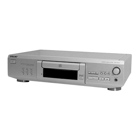
CDP-XE530
Photo : SILVER
SPECIFICATIONS
Maximum
Load
output
impedance
level
2V
Over 10 kΩ
(at 50 kΩ)
–18 dBm
Wave length:
660 nm
32 Ω
10 mW
Model Name Using Similar Mechanism
CD Mechanism Type
Base Unit Type
Optical Pick-up Type
General
Power requirements
220 V – 230 V AC, 50/60 Hz
Power consumption
11W
Dimensions (approx.) 430 × 110 × 290 mm
(17 × 4
× 11
(w/h/d)
3
/
8
Mass (approx.)
3.4 kg (7 lbs 8 oz)
Supplied accessories
Audio cord (2 phono plugs–2 phono plugs) (1)
Remote commander (remote) (1)
R6 (size AA) batteries (2)
Design and specifications are subject to change without notice.
COMPACT DISC PLAYER
AEP Model
UK Model
NEW
CDM14FL-5BD25
BU-5BD25
KSS-213BA/F-NP
1
/
in.) incl. projecting parts
2
Advertisement
Table of Contents

Related Manuals for Sony CDP-XE530


Summary of Contents for Sony CDP-XE530
- Page 1 CDP-XE530 SERVICE MANUAL AEP Model UK Model Photo : SILVER Model Name Using Similar Mechanism CD Mechanism Type CDM14FL-5BD25 Base Unit Type BU-5BD25 Optical Pick-up Type KSS-213BA/F-NP SPECIFICATIONS Compact Disc Player General Laser Semiconductor laser (λ = 780 nm) Power requirements 220 V –...
-
Page 2: Table Of Contents
COMPONENTS IDENTIFIED BY MARK ! OR DOTTED LINE WITH MARK ! ON THE SCHEMATIC DIAGRAMS AND IN THE PARTS LIST ARE CRITICAL TO SAFE OPERATION. REPLACE THESE COMPONENTS WITH SONY PARTS WHOSE PART NUMBERS APPEAR AS SHOWN IN THIS MANUAL OR IN SUPPLEMENTS PUBLISHED BY SONY. -
Page 3: Servicing Note
SECTION 1 SERVICING NOTE HOW TO OPEN THE DISC TRAY WHEN POWER SWITCH NOTES ON HANDLING THE OPTICAL PICK-UP BLOCK TURNS OFF OR BASE UNIT Insert a tapering driver into the aperture of the unit bottom, and turn The laser diode in the optical pick-up block may suffer in the direction of arrow. - Page 4 CD-TEXT TEST DISC This unit is able to display the TEXT data (character information) written in the CD on its fluorescent indicator tube. The CD-TEXT TEST DISC (TGCS-313: J-2501-126-A) is used for checking the display. To check, perform the following procedure. Procedure: Turn ON the power and set the test disc.
- Page 5 Table 2: CD-TEXT TEST DISC Recorded Contents and Display (In this unit, some special characters cannot be displayed. This is not a fault.) TRACK Recorded contents Display ···· ! ” # $ % & are not displayed ! ” # $ % & ´ (21h to 27h)1kHz 0dB L&R + , –...
-
Page 6: General
SECTION 2 GENERAL Front Panel !ª !• !¶ !§ !∞ !¢ !£ !™ !¡ LOCATION OF PARTS AND CONTROLS AMS knob (PUSH ENTER) switch !¡ PHONES jack PLAY MODE button !™ p (stop) button REPEAT button !£ P (pause) button TIME/TEXT button !¢... -
Page 7: Disassembly
SECTION 3 DISASSEMBLY Note : Follow the disassembly procedure in the numerical order given. 3-1. FRONT PANEL • In order to remove the front panel block when the power supply does not turn on, rotate the cam with tapering driver as the figure shows, and the loading part will be moved. -
Page 8: Test Mode
SECTION 4 TEST MODE 4-1. AF MODE Button No. Button No. Button Button The following checks can be performed in the AF mode, which is Displayed Displayed set by connecting the JW617 (AFADJ) terminal on MAIN LANGUAGE board to the Ground and turning on the power. MUSIC SCAN •... - Page 9 4-3. AGING MODE [ MAIN BOARD ] – Component Side – This unit is equipped with an aging mode to check operations of the mechanism deck. • When faults occur: Aging stops, and the state when aging stopped is displayed on the fluorescent display tube.
-
Page 10: Electrical Block Checking
SECTION 5 ELECTRICAL BLOCK CHECKING Note: CD Block is basically designed to operate without adjustment. symmetry Therefore, check each item in order given. S-curve waveform Use YEDS-18 disc (3-702-101-01) unless otherwise indicated. Use an oscilloscope with more than 10MΩ impedance. Clean the object lens by an applicator with neutral detergent Within 3.8 ±... - Page 11 Adjustment Location : 1 track jump waveform Center of the waveform [ MAIN BOARD ] – Component Side – A (DC voltage) + 0.7 CN621 level : 1.3 Vp-p symmetry – 0.6 E-F Balance Check (With general remote commander) oscilloscope BD board JW613 (ADJ) TP (TE)
-
Page 12: Diagrams
SECTION 6 DIAGRAMS 6-1. CIRCUIT BOARDS LOCATION LOADING board BD board POWER SW board KEY board MAIN board DISPLAY board HP board — 12 —... -
Page 13: Schematic Diagram - Loading Motor Section
CDP-XE530 • Waveforms 6-2. SCHEMATIC DIAGRAM – LOADING MOTOR SECTION – THIS NOTE IS COMMON FOR PRINTED WIRING IC101 &¡ XTAI BOARDS AND SCHEMATIC DIAGRAMS. (In addition to this, the necessary note is printed in each block.) 3.9Vp-p For schematic diagrams. -
Page 14: Printed Wiring Board - Bd Section
CDP-XE530 6-4. PRINTED WIRING BOARD – BD SECTION – • See page 12 for Circuit Board Location. (Page 19) A/F-NP — 15 — — 16 —... -
Page 15: Schematic Diagram - Bd Section
CDP-XE530 6-5 SCHEMATIC DIAGRAM – BD SECTION – • See page 13 for Waveforms. • See page 27 for IC Pin Functions. • See page 31 for IC Block Diagrams. A/F-NP (Page 21) (Page 21) A/F-NP A/F-NP (Page 21) — 17 —... -
Page 16: Printed Wiring Board - Main Section
CDP-XE530 6-6. PRINTED WIRING BOARD – MAIN SECTION – • See page 12 for Circuit Board Location. • Semiconductor Location Ref. No. Location D401 D402 D601 D602 D603 D604 D605 E-10 D612 D613 D614 D615 D616 D621 D-12 D631 D641... -
Page 17: Schematic Diagram - Main Section
CDP-XE530 6-7. SCHEMATIC DIAGRAM – MAIN SECTION – • See page 33 for IC Block Diagrams. (Page 17) POWER SW BOARD D614 11ES2 D613 11ES2 S621 CN602 POWER C619 C621 1000µ 4700p C620 4700pF CN601 2P ~AC IN (Page 26) -
Page 18: Printed Wiring Board - Display Section
CDP-XE530 6-8. PRINTED WIRING BOARD – DISPLAY SECTION – • See page 12 for Circuit Board Location. — 23 — — 24 —... -
Page 19: Schematic Diagram - Display Section
CDP-XE530 6-9 SCHEMATIC DIAGRAM – DISPLAY SECTION – • See page 29 for IC Pin Functions. (Page 21) KEY BOARD NO301 NO502 2P — 25 — — 26 —... -
Page 20: Ic Pinfunctions
CDP-XE530 6-10. IC PINFUNCTIONS • IC101 DIGITAL SIGNAL PROCESSOR (CXD2585Q)(BD board) Pin No. Pin Name Function Pin No. Pin Name Function DVDD – Digital power supply Tracking error signal input XRST System reset “L” : reset Center servo analog input MUTE Muting input “H”... - Page 21 • IC501 SYSTEM CONTROL (CXP82832-012Q)(DISPLAY board) Pin No. Pin Name Function FL grid signal output FL grid signal output – Connected to VDD – Power supply (+5V) SCOR Sub code sync input 6, 7 – Power supply RMIN Remote control signal input –...
- Page 22 Pin No. Pin Name Function – Ground – Not used – Connected to ground VDD (+5V) – Power supply (+5V) VFDP (–30V) – Pull down voltage (–30V) XSEL Not used — – Not used LP CONTROL LP control hold output 49 to 66 OPEN –...
-
Page 23: Ic Block Diagrams
6-11. IC BLOCK DIAGRAMS • BD SECTION IC101 CXD2585Q 71 70 67 66 65 64 63 62 61 Digital VPCO Clock DVDD0 V16M Generator XRST VCTL MUTE Interface BIAS Error AVDD1 Corrector DATA XLAT CLOCK FILI Interface Digital Sub Code FILO demodurator Processor... - Page 24 IC102 BA6392FP BUFF CH1 OUT F 28 GND BUFF BUFF CH1 OUT R 27 CH4 OUT F LEVEL SHIFT CAPA IN 1 26 CH4 OUT R BUFF CH1 R IN 25 VB IN INTERFACE CH1 F IN 24 VS IN BUFF VREF IN 23 VB IN...
-
Page 25: Main Section
• MAIN SECTION IC631 LB1641 IC601 LA5602 T.S.D O.C.P V IN MOTOR MOTOR ERROR DRIVE DRIVE REFERENCE VOLTAGE OVER CURRENT LIMITTER FWD/REV/STOP OVER HEAT CONTROL LOGIC PROTECTION ON/OFF RESET CDEL V OUT IC661 CXD8567AM INIT D Vdd 2 SYSM L1 (+) A Vdd L SHIFT L2 (+) - Page 26 SECTION 7 EXPLODED VIEWS NOTE: • -XX, -X mean standardized parts, so they may • The mechanical parts with no reference number • Color Indication of Appearance Parts have some differences from the original one. in the exploded views are not supplied. Example: •...
- Page 27 Description Remarks X-4950-693-1 PANEL ASSY, FRONT(BLACK) 4-210-291-01 SCREW (CASE 3 TP2)(BLACK)(AEP,AED,CIS) X-4950-694-1 PANEL ASSY, FRONT(SILVER) 4-210-291-11 SCREW (CASE 3 TP2)(SILVER)(AEP) 4-996-698-01 EMBLEM, SONY 4-999-877-01 SCREW (CASE)(UK) 4-977-593-11 RING(DIA. 50), ORNAMENTAL 1-776-100-11 WIRE(FLAT TYPE) (23 CORE) 4-977-358-11 CUSHION(AEP,UK,CIS) ! 18 1-575-651-21 CORD, POWER...
-
Page 28: Cd Mechanism Section (Cdm14Fl-5Bd25)
7-2. CD MECHANISM SECTION (CDM14FL-5BD25) BU-5BD25 not supplied M151 Ref. No. Part No. Description Remarks Ref. No. Part No. Description Remarks 1-452-925-21 MAGNET ASSY 1-645-721-11 LOADING BOARD 4-933-134-01 SCREW (+PTPWH M2.6 × 6) 4-933-110-41 HOLDER (MG) 4-995-814-21 TABLE (FL), DISC 4-959-996-01 SPRING (932), COMPRESSION 4-967-268-01 GEAR (C) 4-933-129-01 HOLDER (BU) -
Page 29: Base Unit Section (Bu-5Bd25)
7-3. BASE UNIT SECTION (BU-5BD25) M102 M101 Ref. No. Part No. Description Remarks Ref. No. Part No. Description Remarks ! 151 8-848-379-31 OPTICAL PICK-UP KSS-213BA/F-NP 4-917-564-01 GEAR (P), FLATNESS 1-769-069-11 WIRE (FLAT TYPE) (16 CORE) * 157 A-4724-002-A BD BOARD, COMPLETE 3-713-786-51 SCREW +P 2 ×... -
Page 30: Electrical Parts List
SECTION 8 ELECTRICAL PARTS LIST NOTE: • Due to standardization, replacements in the • CAPACITORS: • SEMICONDUCTORS parts list may be different from the parts uF: µF In each case, u: µ, for example: specified in the diagrams or the components •... - Page 31 DISPLAY LOADING Ref. No. Part No. Description Remarks Ref. No. Part No. Description Remarks A-4724-502-A DISPLAY BOARD, COMPLETE S521 1-762-752-11 SWITCH, TACTILE(§OPEN/CLOSE) S522 1-762-752-11 SWITCH, TACTILE(·) *********************** S523 1-762-752-11 SWITCH, TACTILE(P) 4-997-495-01 GUIDE(FL) S524 1-762-752-11 SWITCH, TACTILE(p) S531 1-475-543-11 ENCODER, ROTARY(AMS) <...
- Page 32 MAIN Ref. No. Part No. Description Remarks Ref. No. Part No. Description Remarks A-4724-503-A MAIN BOARD, COMPLETE(AEP,AED,CIS) C690 1-164-159-11 CERAMIC 0.1uF C691 1-164-159-11 CERAMIC 0.1uF ********************* C695 1-161-494-00 CERAMIC 0.022uF A-4724-507-A MAIN BOARD, COMPLETE(UK) C801 1-162-282-31 CERAMIC 100PF C802 1-161-494-00 CERAMIC 0.022uF ********************* 7-685-871-01 SCREW +BVTT 3 ×...
- Page 33 MAIN Ref. No. Part No. Description Remarks Ref. No. Part No. Description Remarks < IC > R651 1-249-429-11 CARBON 1/4W R661 1-249-417-11 CARBON 1/4W F IC601 8-759-061-65 IC LA5602 R662 1-249-417-11 CARBON 1/4W F IC602 8-749-011-78 IC BA17807T R663 1-249-417-11 CARBON 1/4W F IC631 8-759-822-09 IC LB1641...
- Page 34 CDP-XE530 POWER SW Ref. No. Part No. Description Remarks Ref. No. Part No. Description Remarks 1-672-319-11 POWER SW BOARD ACCESSORIES & PACKING MATERIALS *************** ******************************* 7-685-871-01 SCREW +BVTT 3 × 6 (S) 1-473-720-11 REMOTECOMMANDER (RM-DX50) 1-776-263-11 CORD,CONNECTION (AUDIO) < CAPACITOR >...
Need help?
Do you have a question about the CDP-XE530 and is the answer not in the manual?
Questions and answers