Table of Contents

Related Manuals for Sony CDP-XE510


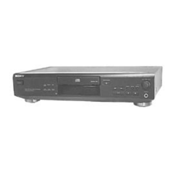
Summary of Contents for Sony CDP-XE510
- Page 1 CDP-XE510 SERVICE MANUAL AEP Model UK Model Photo: BLACK Model Name Using Similar Mechanism CDP-XE500 CD Mechanism Type CDM14-5BD22 Base Unit Type BU-5BD22 Optical Pick-up Type KSS-213BA/F-NP SPECIFICATIONS COMPACT DISC PLAYER MICROFILM — 1 —...
-
Page 2: Table Of Contents
WITH MARK ! ON THE SCHEMATIC DIAGRAMS AND IN THE PARTS LIST ARE CRITICAL TO SAFE OPERATION. REPLACE THESE COMPONENTS WITH SONY PARTS WHOSE PART NUMBERS APPEAR AS SHOWN IN THIS MANUAL OR IN SUPPLEMENTS PUBLISHED BY SONY. — 2 —... -
Page 3: Servicing Note
SECTION 1 SERVICING NOTE HOW TO OPEN THE DISC TRAY WHEN POWER SWITCH CD-TEXT TEST DISC TURNS OFF This unit is able to display the text data (character information) Insert a tapering driver into the aperture of the unit bottom, and turn written in the CD on its fluorescent indicator tube. -
Page 4: General
SECTION 2 GENERAL LOCATION OF PARTS AND CONTROLS Front Panel 8 9 0 !¡ !• !ª !¶ !§ !∞ !¢ !£ !™ 1 POWER switch !¡ ≠ AMS* ± knob 2 PLAY MODE button !™ PHONES jack 3 REPEAT button !£... -
Page 5: Disassembly
SECTION 3 DISASSEMBLY Note : Follow the disassembly procedure in the numerical order given. 3-1. FRONT PANEL • In order to remove the front panel block when the power supply does not turn on, rotate the cam with tapering driver as the figure shows, and the loading part will be moved. -
Page 6: Test Mode
SECTION 4 TEST MODE 4-1. AF MODE Button No. Button No. Button Button The following checks can be performed in the AF mode, which is Displayed Displayed set by connecting the TP2 (AFADJ) terminal on MAIN CHECK PLAY MODE board to the Ground and turning on the power. REPEAT •... - Page 7 4-2. ADJ MODE [ MAIN BOARD ] — Component Side — The following operations are performed in the ADJ mode, which is set by connecting the TP1 (ADJ) terminal to the Ground and turning on the power. IC631 • During playback, there is no problem even if the GFS is continu- ously LOW.
-
Page 8: Electrical Block Checking
SECTION 5 ELECTRICAL BLOCK CHECKING Note: Note: 1. CD Block is basically designed to operate without adjustment. A clear RF signal waveform means that the shape “◊” can be clearly Therefore, check each item in order given. distinguished at the center of the waveform. 2. - Page 9 RF PLL Free-run Frequency Check 6. Check the level B of the oscilliscope's waveform and the A (DC voltage) of the center of the Traverse waveform. Procedure : Confirm the following : 1. Connect frequency counter to test point (PLCK) with lead wire. A/B x 100 = less than ±...
-
Page 10: Diagrams
SECTION 6 DIAGRAMS 6-1. IC BLOCK DIAGRAMS IC101 CXD2545Q 67 62 63 64 20 19 32K RAM CLOCK GENERATOR C16M 43 PSSL DIGITAL ADDRESS PRIORITY VCO1 SERIAL GENERATOR ENCODER VCO0 PARALLEL DEMODULATOR VARI-PITCH 61-46 DA01-16 DOUBLE SPEED PROCESSOR FILI FILO 79 MUTE SYNC CLTV... - Page 11 IC103 CXA1821M-T6 LD ON LC/PD APC LD AMP VREF RF EQ AMP RF SUMMING AMP FOCUS ERROR AMP FE BIAS TRACKING ERROR AMP VC BUFFER IC104 LC89170M-TLM EXCK CPU INTERFACE SBSO DQSY 32 WORD X 8 BIT CHECKER DUAL PORT RAM SCOR SRDT WFCK...
- Page 12 IC631 LB1641 T.S.D O.C.P MOTOR MOTOR DRIVE DRIVE FWD/REV/STOP CONTROL LOGIC IC661 CXD8567AM INIT D Vdd 2 SYSM L1 (+) A Vdd L SHIFT L2 (+) LATCH A Vss L 256FSO X Vss TEST1 512IN D Vss X OUT MCKSEL X Vdd XBCK A Vss R...
-
Page 13: Circuit Boards Location
CDP-XE510 • Waveforms THIS NOTE IS COMMON FOR PRINTED WIRING BOARDS 6-2. CIRCUIT BOARDS LOCATION AND SCHEMATIC DIAGRAMS. (In addition to this, the necessary note is printed in each block.) 1.3Vp-p • Printed wiring boards. • : parts extracted from the component side. -
Page 21: Ic Pin Functions
6-11. IC PIN FUNCTIONS • IC501 FL DRIVER CONTROL (MSM9202-03GK-BK) Pin No. Pin Name Function Fluorescent display tube anode electrodedrive output terminal Fluorescent display tube anode electrodedrive output terminal Fluorescent display tube anode electrodedrive output terminal Fluorescent display tube anode electrodedrive output terminal Fluorescent display tube anode electrodedrive output terminal Fluorescent display tube anode electrodedrive output terminal Fluorescent display tube anode electrodedrive output terminal... - Page 22 Pin No. Function Pin Name Fluorescent display tube grid electrodedrive output terminal Fluorescent display tube grid electrodedrive output terminal Fluorescent display tube grid electrodedrive output terminal uorescent display tube grid electrodedrive output terminal Fluorescent display tube grid electrodedrive output terminal Fluorescent display tube grid electrodedrive output terminal Fluorescent display tube grid electrodedrive output terminal Fluorescent display tube drive power supply...
- Page 23 • IC621 SYSTEM CONTROL (CXP84332-036Q) Pin No. Pin Name Function Not used Not used Not used Not used Not used Not used Not used Not used Not used Not used Not used Not used Not used Not used Not used Not used Not used Not used...
- Page 24 Pin No. Pin Name Function LOAD IN. SW Loading in switch input Not used Key input KEY 1 KEY 0 Key input Type switching and test mode input ADJ/AFJ BUSIN CONTROL-A1 input L: Active Latch for fluorenscent indicator driver IC Clock for servo IC and digital filter IC LDON Laser diode control H: ON...
-
Page 25: Exploded Views
* 17 4-987-946-11 PANEL, BACK (UK) X-4947-901-2 PANEL ASSY, FRONT (SILVER) * 18 A-4699-485-A MAIN BOARD, COMPLETE (AEP,EE,CIS) 4-963-404-21 EMBLEM (5-A), SONY * 18 A-4699-599-A MAIN BOARD, COMPLETE (UK) 4-977-593-01 RING (DIA. 50), ORNAMENTAL * 19 3-349-025-41 HOLDER, PC BOARD... -
Page 26: Mechanism Deck Section (Cdm14-5Bd22)
7-2. MECHANISM DECK SECTION (CDM14-5BD22) BU-5BD22 not supplied not supplied M151 Ref. No. Part No. Description Remark Ref. No. Part No. Description Remark * 101 1-452-538-11 MAGNET 4-933-134-01 SCREW +PTPWH M2.6X6 4-933-110-41 HOLDER (MG) 4-933-112-11 TABLE, DISC 4-959-996-01 SPRING (932), COMPRESSION 4-967-268-01 GEAR (C) 4-933-129-01 HOLDER (BU) 4-927-649-01 BELT... -
Page 27: Base Unit Section (Bu-5Bd22)
7-3. BASE UNIT SECTION (BU-5BD22) M102 M101 The components identified by mark ! or dotted line with mark ! are critical for safety. Replace only with part number speci- fied. Ref. No. Part No. Description Remark Ref. No. Part No. Description Remark ! 151... -
Page 28: Electrical Parts List
SECTION 8 ELECTRICAL PARTS LIST Note: • SEMICONDUCTORS • Due to standardization, replacements in the parts list The components identified by mark ! In each case, u: µ , for example: may be different from the parts specified in the or dotted line with mark ! are critical uA...: µ... - Page 29 LOADING MAIN Ref. No. Part No. Description Remark Ref. No. Part No. Description Remark 1-664-312-11 HP BOARD C623 1-161-494-00 CERAMIC 0.022uF C626 1-162-282-31 CERAMIC 100PF ******** C631 1-161-494-00 CERAMIC 0.022uF 7-611-031-11 WIRE, TINNING COPPER C632 1-162-306-11 CERAMIC 0.01uF < CAPACITOR > C633 1-161-494-00 CERAMIC 0.022uF...
- Page 30 MAIN Ref. No. Part No. Description Remark Ref. No. Part No. Description Remark < DIODE > Q683 8-729-922-37 TRANSISTOR 2SD2144S Q691 8-729-029-56 TRANSISTOR DTA144ESA D601 8-719-200-82 DIODE 11ES2 Q692 8-729-922-37 TRANSISTOR 2SD2144S Q693 8-729-922-37 TRANSISTOR 2SD2144S D602 8-719-200-82 DIODE 11ES2 D603 8-719-200-82 DIODE 11ES2 D604...
- Page 31 MAIN PANEL POWER SW Ref. No. Part No. Description Remark Ref. No. Part No. Description Remark R908 1-249-419-11 CARBON 1.5K 1/4W F R515 1-249-421-11 CARBON 2.2K 1/4W F R909 1-249-441-11 CARBON 100K 1/4W R516 1-247-843-11 CARBON 3.3K 1/4W R910 1-249-414-11 CARBON 1/4W F R517 1-249-427-11 CARBON...
- Page 32 CDP-XE510 Ref. No. Part No. Description Remark MISCELLANEOUS ************** 1-769-971-11 WIRE (FLAT TYPE)(13 CORE) 1-776-100-11 WIRE (FLAT TYPE)(23 CORE) ! 24 1-575-651-21 CORD, POWER (AEP,EE,CIS) ! 24 1-696-907-11 CORD, POWER (UK) * 101 1-452-538-11 MAGNET ! 151 8-848-379-31 OPTICAL PICK-UP KSS-213BA/F-NP...
Need help?
Do you have a question about the CDP-XE510 and is the answer not in the manual?
Questions and answers