Table of Contents
Advertisement
Quick Links
This user's guide describes the operational use of the TPS7A8901EVM-853 evaluation module (EVM) as
a reference design for engineering demonstration and evaluation of the TPS7A8901RTJ, dual low-noise,
low-dropout voltage regulator (LDO). Included in this user's guide are setup and operating instructions,
thermal and layout guidelines, a printed circuit board (PCB) layout, a schematic diagram, and a bill of
materials (BOM).
Throughout this document, the terms demonstration kit, evaluation board, evaluation module are
synonymous with the TPS7A8901EVM-853.
The following related documents are available through the Texas Instruments web site at
http://www.ti.com.
SBVU037 – November 2016
Submit Documentation Feedback
TPS7A89 Evaluation Module
Related Documentation
Device
TPS7A89
Copyright © 2016, Texas Instruments Incorporated
SBVU037 – November 2016
Literature Number
SBVS280
TPS7A89 Evaluation Module
User's Guide
1
Advertisement
Table of Contents

Related Manuals for Texas Instruments TPS7A89


Summary of Contents for Texas Instruments TPS7A89
- Page 1 (PCB) layout, a schematic diagram, and a bill of materials (BOM). Throughout this document, the terms demonstration kit, evaluation board, evaluation module are synonymous with the TPS7A8901EVM-853. The following related documents are available through the Texas Instruments web site at http://www.ti.com. Related Documentation Device...
-
Page 2: Table Of Contents
Layer 3 Routing ..................... Bottom Layer Routing ........................Schematic List of Tables ......................Bill of Materials Trademarks All trademarks are the property of their respective owners. TPS7A89 Evaluation Module SBVU037 – November 2016 Submit Documentation Feedback Copyright © 2016, Texas Instruments Incorporated... -
Page 3: Introduction
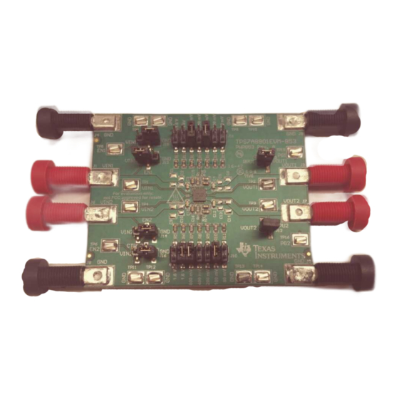
The Texas Instruments TPS7A8901EVM-853 EVM helps design engineers evaluate the operation and performance of the TPS7A89 linear regulator for possible use in their own circuit application. This particular EVM configuration contains a dual low-noise, high-PSRR linear regulator, ideal for high- performance signal chain. -
Page 4: Evm Setup
J10 – ANYOUT2 The channel-2 output voltage of the TPS7A89 is selectable in accordance with the names given to the output voltage setting pins: 50 mV, 100 mV, 200 mV, 400 mV, 800 mV, 1.6 V, and 1.6 V. For each pin connected to the ground, the output voltage setting increases by the value associated with that pin name, starting from the value of the reference voltage of 0.8 V;... - Page 5 J11 – ANYOUT1 The channel-1 output voltage of the TPS7A89 is selectable in accordance with the names given to the output voltage setting pins: 50 mV, 100 mV, 200 mV, 400 mV, 800 mV, 1.6 V, and 1.6 V. For each pin connected to the ground, the output voltage setting increases by the value associated with that pin name, starting from the value of the reference voltage of 0.8 V;...
- Page 6 TP10 – GND Ground. 2.1.27 TP11 – GND Ground. 2.1.28 TP12 – GND Ground. 2.1.29 TP13 – GND Ground. 2.1.30 TP14 – GND Ground. TPS7A89 Evaluation Module SBVU037 – November 2016 Submit Documentation Feedback Copyright © 2016, Texas Instruments Incorporated...
-
Page 7: Soldering Guidelines
3. Enable the channel 2 output by shorting the EN2 pin to VIN2 on J14. 4. Vary the respective load and input voltage, as necessary, for test purposes. SBVU037 – November 2016 TPS7A89 Evaluation Module Submit Documentation Feedback Copyright © 2016, Texas Instruments Incorporated... -
Page 8: Pcb Layout
PCB Layout www.ti.com PCB Layout Figure 1 Figure 5 illustrate the PCB layout for this EVM. Figure 1. Assembly Layer Figure 2. Top Layer Routing TPS7A89 Evaluation Module SBVU037 – November 2016 Submit Documentation Feedback Copyright © 2016, Texas Instruments Incorporated... -
Page 9: Layer 2 Routing
PCB Layout www.ti.com Figure 3. Layer 2 Routing Figure 4. Layer 3 Routing SBVU037 – November 2016 TPS7A89 Evaluation Module Submit Documentation Feedback Copyright © 2016, Texas Instruments Incorporated... -
Page 10: Bottom Layer Routing
PCB Layout www.ti.com Figure 5. Bottom Layer Routing TPS7A89 Evaluation Module SBVU037 – November 2016 Submit Documentation Feedback Copyright © 2016, Texas Instruments Incorporated... -
Page 11: Schematic
Schematic www.ti.com Schematic Figure 6 is the schematic for this EVM. Figure 6. Schematic SBVU037 – November 2016 TPS7A89 Evaluation Module Submit Documentation Feedback Copyright © 2016, Texas Instruments Incorporated... -
Page 12: Bill Of Materials
Fiducial mark. There is nothing to buy or mount. Fiducial Unless otherwise noted in the Alternate Part Number or Alternate Manufacturer columns, all parts may be substituted with equivalents. TPS7A89 Evaluation Module SBVU037 – November 2016 Submit Documentation Feedback Copyright © 2016, Texas Instruments Incorporated... - Page 13 STANDARD TERMS AND CONDITIONS FOR EVALUATION MODULES Delivery: TI delivers TI evaluation boards, kits, or modules, including demonstration software, components, and/or documentation which may be provided together or separately (collectively, an “EVM” or “EVMs”) to the User (“User”) in accordance with the terms and conditions set forth herein.
- Page 14 FCC Interference Statement for Class B EVM devices NOTE: This equipment has been tested and found to comply with the limits for a Class B digital device, pursuant to part 15 of the FCC Rules. These limits are designed to provide reasonable protection against harmful interference in a residential installation.
- Page 15 【無線電波を送信する製品の開発キットをお使いになる際の注意事項】 開発キットの中には技術基準適合証明を受けて いないものがあります。 技術適合証明を受けていないもののご使用に際しては、電波法遵守のため、以下のいずれかの 措置を取っていただく必要がありますのでご注意ください。 1. 電波法施行規則第6条第1項第1号に基づく平成18年3月28日総務省告示第173号で定められた電波暗室等の試験設備でご使用 いただく。 2. 実験局の免許を取得後ご使用いただく。 3. 技術基準適合証明を取得後ご使用いただく。 なお、本製品は、上記の「ご使用にあたっての注意」を譲渡先、移転先に通知しない限り、譲渡、移転できないものとします。 上記を遵守頂けない場合は、電波法の罰則が適用される可能性があることをご留意ください。 日本テキサス・イ ンスツルメンツ株式会社 東京都新宿区西新宿6丁目24番1号 西新宿三井ビル 3.3.3 Notice for EVMs for Power Line Communication: Please see http://www.tij.co.jp/lsds/ti_ja/general/eStore/notice_02.page 電力線搬送波通信についての開発キットをお使いになる際の注意事項については、次のところをご覧ください。http:/ /www.tij.co.jp/lsds/ti_ja/general/eStore/notice_02.page SPACER EVM Use Restrictions and Warnings: 4.1 EVMS ARE NOT FOR USE IN FUNCTIONAL SAFETY AND/OR SAFETY CRITICAL EVALUATIONS, INCLUDING BUT NOT LIMITED TO EVALUATIONS OF LIFE SUPPORT APPLICATIONS.
- Page 16 Notwithstanding the foregoing, any judgment may be enforced in any United States or foreign court, and TI may seek injunctive relief in any United States or foreign court. Mailing Address: Texas Instruments, Post Office Box 655303, Dallas, Texas 75265 Copyright © 2016, Texas Instruments Incorporated...
- Page 17 IMPORTANT NOTICE Texas Instruments Incorporated and its subsidiaries (TI) reserve the right to make corrections, enhancements, improvements and other changes to its semiconductor products and services per JESD46, latest issue, and to discontinue any product or service per JESD48, latest issue.
Need help?
Do you have a question about the TPS7A89 and is the answer not in the manual?
Questions and answers