Table of Contents
Advertisement
Quick Links
www.ti.com
User's Guide
TPS7A53EVM-080 Evaluation Module
This user's guide describes the operational use of the TPS7A53EVM-080 evaluation module (EVM) as
a reference design for engineering demonstration and evaluation of the TPS7A53A-Q1 low-dropout linear
regulator (LDO). Included in this user's guide are setup and operating instructions, thermal and layout guidelines,
a printed circuit board (PCB) layout, a schematic diagram, and a bill of materials (BOM).
Throughout this document, the terms evaluation board, evaluation module, and EVM are synonymous with the
TPS7A53EVM-080.
SBVU078 – NOVEMBER 2022
Submit Document Feedback
ABSTRACT
TPS7A53EVM-080 Evaluation Module
Copyright © 2022 Texas Instruments Incorporated
TPS7A53EVM-080 Evaluation Module
1
Advertisement
Table of Contents

Subscribe to Our Youtube Channel
Related Manuals for Texas Instruments TPS7A53EVM-080


Summary of Contents for Texas Instruments TPS7A53EVM-080
- Page 1 ABSTRACT TPS7A53EVM-080 Evaluation Module This user's guide describes the operational use of the TPS7A53EVM-080 evaluation module (EVM) as a reference design for engineering demonstration and evaluation of the TPS7A53A-Q1 low-dropout linear regulator (LDO). Included in this user's guide are setup and operating instructions, thermal and layout guidelines, a printed circuit board (PCB) layout, a schematic diagram, and a bill of materials (BOM).
-
Page 2: Table Of Contents
List of Figures Figure 2-1. TPS7A53EVM-080 Turn-On............................5 Figure 2-2. TPS7A53EVM-080 With Current Probes Attached....................Figure 2-3. TPS7A53EVM-080 Load Transient Results: 1-mA to 3-A Load Step................7 Figure 2-4. TPS7A53EVM-080 Load Transient Results: 3-A to 1-mA Load Step................7 Figure 3-1. Top Assembly Layer and Silkscreen......................... -
Page 3: Introduction
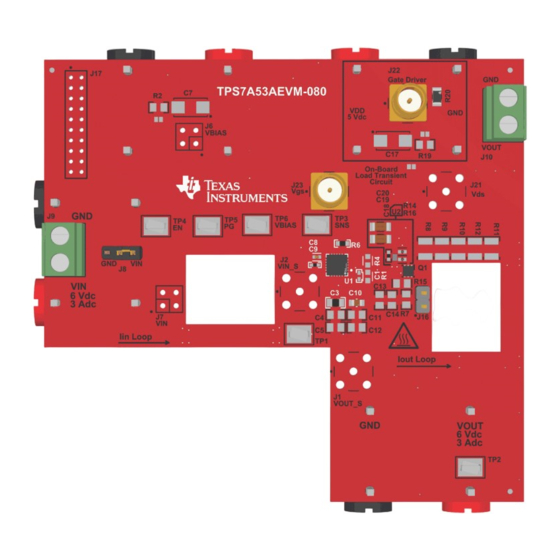
Introduction 1 Introduction The Texas Instruments TPS7A53EVM-080 evaluation module (EVM) helps designers evaluate the operation and performance of the TPS7A53A-Q1 LDO voltage regulator. As shown in Table 1-1, the TPS7A53EVM-080 contains one TPS7A53A-Q1 LDO voltage regulator in the RTJ package. An optional load transient circuit is also included to assist the user with high-speed load transient testing. -
Page 4: Optional Load Transient Input/Output Connector Descriptions
2.2.7 J24 J24 is the jumper used to enable the gate driver device. Tie this pin to GND to enable the gate driver. TPS7A53EVM-080 Evaluation Module SBVU078 – NOVEMBER 2022 Submit Document Feedback Copyright © 2022 Texas Instruments Incorporated... -
Page 5: Tps7A53A-Q1 Ldo Operation And Component Selection
TPS7A53A-Q1 LDO after VIN is applied. Figure 2-1 shows the result of the TPS7A53EVM-080 during turn-on. The yellow trace is the input voltage, the green trace is the load current, and the red trace is the output voltage. Figure 2-1. TPS7A53EVM-080 Turn-On SBVU078 –... -
Page 6: Optional Load Transient Circuit Operation
Optional kelvin sense points are provided using the SMA connectors J2 (VIN) and J1 (VOUT). 2.4 Optional Load Transient Circuit Operation The TPS7A53EVM-080 evaluation module contains an optional high-performance load transient circuit to allow efficient testing of the TPS7A53A-Q1 LDO load transient performance. To use the optional load transient circuit, install the correct components in accordance with the application. -
Page 7: Figure 2-3. Tps7A53Evm-080 Load Transient Results: 1-Ma To 3-A Load Step
The resulting test data shows a 1-mA to 3-A load step on VOUT of the LDO, with only a 47-μF capacitor on the output of the LDO. Figure 2-3. TPS7A53EVM-080 Load Transient Figure 2-4. TPS7A53EVM-080 Load Transient Results: 1-mA to 3-A Load Step Results: 3-A to 1-mA Load Step SBVU078 –... -
Page 8: Board Layout
TPS7A53EVM-080 PCB. The TPS7A53EVM-080 dissipates power, which can cause some components to experience an increase in temperature. The TPS7A53A-Q1 LDO and pulsed resistors R8, R9, R10, R11, and R12 are most at risk of raising the junction temperature during normal operation. -
Page 9: Figure 3-5. Layer 4
Board Layout Figure 3-5. Layer 4 Figure 3-6. Layer 5 Figure 3-8. Bottom Assembly Layer and Silkscreen Figure 3-7. Bottom Layer Routing SBVU078 – NOVEMBER 2022 TPS7A53EVM-080 Evaluation Module Submit Document Feedback Copyright © 2022 Texas Instruments Incorporated... -
Page 10: Tps7A53Evm-080 Schematic
TPS7A53EVM-080 Schematic www.ti.com 4 TPS7A53EVM-080 Schematic Figure 4-1 shows a schematic for the TPS7A53EVM-080. Vin Recommended Max = 6V BIAS Recommended Max = 6V Vout Max = 3.6V BIAS Iout Max = 3A 1000pF BI AS 10µF 10µF 10µF 330uF 10µF... -
Page 11: Bill Of Materials
TPS7A53EVM-080 Schematic 5 Bill of Materials Table 5-1 shows the bill of materials (BOM) for the TPS7A53EVM-080. Table 5-1. Bill of Materials Designator Quantity Value Description PackageReference PartNumber Manufacturer !PCB1 Printed Circuit Board LP080 10 µF CAP CER 10 µF 10V X7R 0805... - Page 12 STANDARD TERMS FOR EVALUATION MODULES Delivery: TI delivers TI evaluation boards, kits, or modules, including any accompanying demonstration software, components, and/or documentation which may be provided together or separately (collectively, an “EVM” or “EVMs”) to the User (“User”) in accordance with the terms set forth herein.
- Page 13 www.ti.com Regulatory Notices: 3.1 United States 3.1.1 Notice applicable to EVMs not FCC-Approved: FCC NOTICE: This kit is designed to allow product developers to evaluate electronic components, circuitry, or software associated with the kit to determine whether to incorporate such items in a finished product and software developers to write software applications for use with the end product.
- Page 14 www.ti.com Concernant les EVMs avec antennes détachables Conformément à la réglementation d'Industrie Canada, le présent émetteur radio peut fonctionner avec une antenne d'un type et d'un gain maximal (ou inférieur) approuvé pour l'émetteur par Industrie Canada. Dans le but de réduire les risques de brouillage radioélectrique à...
- Page 15 www.ti.com EVM Use Restrictions and Warnings: 4.1 EVMS ARE NOT FOR USE IN FUNCTIONAL SAFETY AND/OR SAFETY CRITICAL EVALUATIONS, INCLUDING BUT NOT LIMITED TO EVALUATIONS OF LIFE SUPPORT APPLICATIONS. 4.2 User must read and apply the user guide and other available documentation provided by TI regarding the EVM prior to handling or using the EVM, including without limitation any warning or restriction notices.
- Page 16 Notwithstanding the foregoing, any judgment may be enforced in any United States or foreign court, and TI may seek injunctive relief in any United States or foreign court. Mailing Address: Texas Instruments, Post Office Box 655303, Dallas, Texas 75265 Copyright © 2019, Texas Instruments Incorporated...
- Page 17 TI products. TI’s provision of these resources does not expand or otherwise alter TI’s applicable warranties or warranty disclaimers for TI products. TI objects to and rejects any additional or different terms you may have proposed. IMPORTANT NOTICE Mailing Address: Texas Instruments, Post Office Box 655303, Dallas, Texas 75265 Copyright © 2022, Texas Instruments Incorporated...
Need help?
Do you have a question about the TPS7A53EVM-080 and is the answer not in the manual?
Questions and answers