Table of Contents
Advertisement
Quick Links
Advertisement
Table of Contents

Subscribe to Our Youtube Channel
Related Manuals for Lattice Semiconductor iCE40 Ultra


Summary of Contents for Lattice Semiconductor iCE40 Ultra
- Page 1 Ultra™ Breakout Board User Guide December 2014 EB87_1.1...
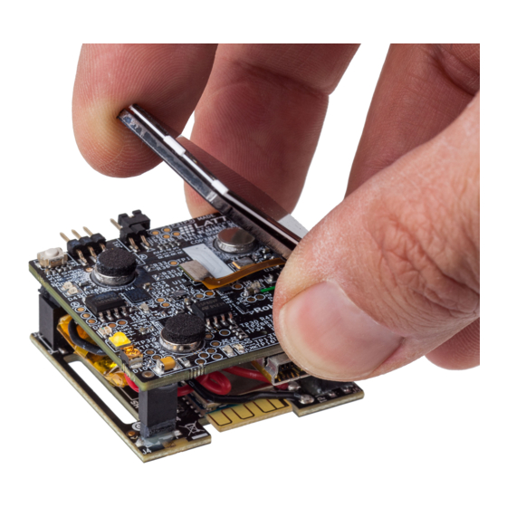
- Page 2 This guide describes how to begin using the iCE40 Ultra Breakout Board, an easy-to-use platform for demonstrat- ing the high-current LED drive capabilities of the iCE40 Ultra FPGA. Along with the evaluation board and accesso- ries, this kit includes the pre-loaded LED Driver Demo that demonstrates driving the RGB LEDs with a PWM circuit.
-
Page 3: Software Requirements
Ultra Breakout Board Figure 1 shows the top side of the iCE40 Ultra Breakout Board indicating the specific features that are designed on the board. Figure 1. iCE40 Ultra Breakout Board (Top Side) D3 – USB Interface Power LED... - Page 4 Ultra Breakout Board Demonstration Design Shunts Lattice provides the RGB LED Driver Demo design programmed in the board. The RGB LED Driver Demo used in conjunction with the software GUI illustrates the use of a PWM driver controlling the LEDs on the board. Below is a description of the control jumpers for each LED.
-
Page 5: Clock Sources
— ICC2 can be measured across the series resistor R15 (1Ohm) at TP3 and TP4 The power supplies on the iCE40 Ultra Breakout Board are simplified and suitable for booting from the external SPI flash. The power supply sequencing does not conform to the NVCM boot requirements as specified in DS1048, iCE40 Ultra Family Data Sheet. - Page 6 Ultra Breakout Board Figure 3. Configuration and Programming Details USB Interface CRESETB Socket Push-Button J2 CRESETB Probe – D2 – DONE LED J10 – Program SPI Flash or iCE5LP J9 – Isolate U8 – SPI Flash CSn iCE5LP4K - SWG36 U7 –...
-
Page 7: Test Points
Ultra Breakout Board Test Points The board features a number of headers and test connections which provide access to the iCE40 Ultra I/Os: Figure 4. J6 Header ‘A’ Breakouts HEADER A Figure 5. J7 Header ‘B’ Breakouts HEADER B Figure 6. - Page 8 Ultra Breakout Board Figure 7. J7 Header ‘B’ Breakouts AARDVARK CONNECTOR The break-out headers and test connectors are shown in Figure 8. Figure 8. Breakout Headers J1 – Aardvark SPI emulator connector J6 – “Header A” J7 – “Header B”...
-
Page 9: Rgb Led Demonstration Design And Software Gui
Ultra Breakout Board RGB LED Demonstration Design and Software GUI The iCE40 Ultra Breakout Board can demonstrate a complete controller for an RGB LED. These are the steps nec- essary to run the demonstration. 1. Ensure that the RGB LED GUI is installed. - Page 10 Ultra Breakout Board 4. After the iCE40 Ultra device has initialized and the RGB LED is illuminated RED, change the J10 jumper posi- tions to horizontal, shorting pins 1-2 and 3-4. This is required to allow the USB port to communicate with the iCE40 Ultra device.
- Page 11 GUI Serial Communication Interface LED Control via SPI The Software GUI demonstration program communicates with the iCE40 Ultra device using a SPI serial communi- cation channel. The SPI interface (mode 0) control link is implemented using a simple write-only protocol (see Figure 12).
-
Page 12: Register Definitions
Ultra Breakout Board Register Definitions Default setting (hardware, software) is denoted by (*). RGB Color[3:0] Color Color Code 0000* #FF0000 0001 Orange #FF7F00 0010 Yellow #FFFF00 0011 Chartreuse #7FFF00 0100 Green #00FF00 0101 Spring Green #00FF7F 0110 Cyan #00FFFF... - Page 13 Breathe Ramp [3:0] Factor 0000* .0x (fast) 0001 .063x 0010 .125x 0011 .25x 0100 0101 0110 0111 4x (slow) 1000 — — 1001 1010 — 1011 — — 1100 1101 — 1110 — 1111 — Blink Rate [3:0] Off Time (s) 0000 Always On 0001...
-
Page 14: Ordering Information
01.0 Initial release. © 2014 Lattice Semiconductor Corp. All Lattice trademarks, registered trademarks, patents, and disclaimers are as listed at www.latticesemi.com/legal. All other brand or product names are trademarks or registered trademarks of their respective holders. The specifications and information herein are subject to change without notice. -
Page 15: Appendix A. Schematic Diagrams
Appendix A. Schematic Diagrams Figure 13. Block Diagram BANK 1... - Page 16 Figure 14. FTDI Connection...
- Page 17 Figure 15. DUT Connection...
- Page 18 Figure 16. LEDs and Headers...
- Page 19 Figure 17. Regulator Connection...
- Page 20 Figure 18. SPI...
-
Page 21: Appendix B. Bill Of Materials
Ultra Breakout Board Appendix B. Bill of Materials Item Reference Quantity Part PCB Footprint PART_NUMBER Description C1,C3,C33 4.7uF cc0603 ECJ-1VB0J475K Panasonic CAP CER 4.7UF 6.3 V 10% X5R 0603 C2, C4, C5, C6, C7, C8, C9, 0.1uF cc0603 C0603C104K4RACTU Kemet CAP CER 0.1UF 16 V 10% X7R 0603... - Page 22 Ultra Breakout Board Item Reference Quantity Part PCB Footprint PART_NUMBER Description ICE5LP4KSWG36 36_WLCSP LED TRI- 6-PLCC SFT722N-S Seoul Semicon- LED RED/GRN/BLU CLEAR LENS 6PLCC COLOUR_1 ductor Inc 12.0000 MHZ osc_4p_dsc3001 DSC3001HE2- Mircel OSCILLATOR 12.0000 MHZ -20'C to 70'C +/- 012.0000T...
Need help?
Do you have a question about the iCE40 Ultra and is the answer not in the manual?
Questions and answers