Table of Contents
Advertisement
Quick Links
Advertisement
Table of Contents

Related Manuals for Lattice Semiconductor iCE40HX-8K


Summary of Contents for Lattice Semiconductor iCE40HX-8K
- Page 1 Breakout Board Evaluation Board User Guide FPGA-EB-02031-1.2 July 2020...
- Page 2 The information provided in this document is proprietary to Lattice Semiconductor, and Lattice reserves the right to make any changes to the information in this document or to any products at any time without notice.
-
Page 3: Table Of Contents
Table 9.1. Ordering Information ............................10 © 2013-2020 Lattice Semiconductor Corp. All Lattice trademarks, registered trademarks, patents, and disclaimers are as listed at www.latticesemi.com/legal. All other brand or product names are trademarks or registered trademarks of their respective holders. The specifications and information herein are subject to change without notice. -
Page 4: Acronyms In This Document
Serial Peripheral Interface © 2013-2020 Lattice Semiconductor Corp. All Lattice trademarks, registered trademarks, patents, and disclaimers are as listed at www.latticesemi.com/legal. All other brand or product names are trademarks or registered trademarks of their respective holders. The specifications and information herein are subject to change without notice. -
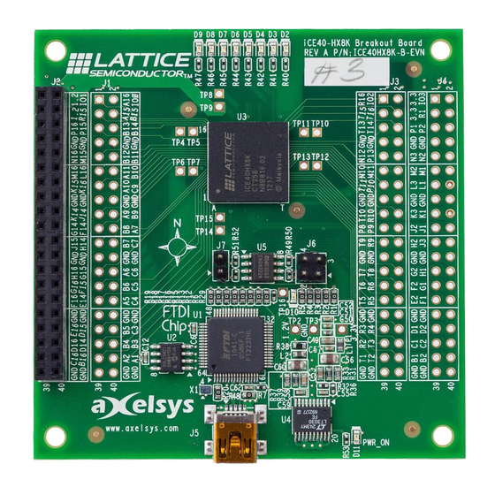
Page 5: Introduction
Pre-loaded Demo – The kit comes with a default design that flashes the LEDs on and off. USB connector Cable – A mini B USB cable for programming the SRAM fabric of the iCE40HX-8K or the onboard SPI flash. The USB cable also powers the iCE40HX-8K evaluation board. -
Page 6: Figure 2.2. Block Diagram
Figure 2.2. Block Diagram © 2013-2020 Lattice Semiconductor Corp. All Lattice trademarks, registered trademarks, patents, and disclaimers are as listed at www.latticesemi.com/legal. All other brand or product names are trademarks or registered trademarks of their respective holders. The specifications and information herein are subject to change without notice. -
Page 7: Ice40 Device
Evaluation Board User Guide 3. iCE40 Device This board features an iCE40HX-8K device with a 1.2 V core supply. It is packaged in a 256 caBGA package. For a iCE40 LP/HX Family Data Sheet complete description of this device, refer to (FPGA-DS-02029). -
Page 8: Board Power
6. Board Power The iCE40HX-8K evaluation board is powered with the USB cable. LED location D11 indicates that the board is powered up. All I/O are driven at 3.3 V. There are two versions of the BOM. Early versions have D1 populated with a CDBU0520 Schottky. -
Page 9: Figure 8.2. Cram Programming
8.2. Figure 8.2. CRAM Programming LED in location D10 is connected to the CDONE pin of the iCE40HX-8K. This can be monitored to determine that the iCE40HX-8K is programmed correctly. © 2013-2020 Lattice Semiconductor Corp. All Lattice trademarks, registered trademarks, patents, and disclaimers are as listed at www.latticesemi.com/legal. -
Page 10: Ordering Information
© 2013-2020 Lattice Semiconductor Corp. All Lattice trademarks, registered trademarks, patents, and disclaimers are as listed at www.latticesemi.com/legal. All other brand or product names are trademarks or registered trademarks of their respective holders. The specifications and information herein are subject to change without notice. -
Page 11: Technical Support Assistance
Submit a technical support case through www.latticesemi.com/techsupport. © 2013-2020 Lattice Semiconductor Corp. All Lattice trademarks, registered trademarks, patents, and disclaimers are as listed at www.latticesemi.com/legal. All other brand or product names are trademarks or registered trademarks of their respective holders. The specifications and information herein are subject to change without notice. -
Page 12: Appendix A. Schematic Diagrams
Figure A.1. Block Diagram © 2013-2020 Lattice Semiconductor Corp. All Lattice trademarks, registered trademarks, patents, and disclaimers are as listed at www.latticesemi.com/legal. All other brand or product names are trademarks or registered trademarks of their respective holders. The specifications and information herein are subject to change without notice. -
Page 13: Figure A.2. Usb To Spi/Rs232
Figure A.2. USB to SPI/RS232 © 2013-2020 Lattice Semiconductor Corp. All Lattice trademarks, registered trademarks, patents, and disclaimers are as listed at www.latticesemi.com/legal. All other brand or product names are trademarks or registered trademarks of their respective holders. The specifications and information herein are subject to change without notice. -
Page 14: Figure A.3. Fpga
Figure A.3. FPGA © 2013-2020 Lattice Semiconductor Corp. All Lattice trademarks, registered trademarks, patents, and disclaimers are as listed at www.latticesemi.com/legal. All other brand or product names are trademarks or registered trademarks of their respective holders. The specifications and information herein are subject to change without notice. -
Page 15: Figure A.4. Fpga
Figure A.4. FPGA © 2013-2020 Lattice Semiconductor Corp. All Lattice trademarks, registered trademarks, patents, and disclaimers are as listed at www.latticesemi.com/legal. All other brand or product names are trademarks or registered trademarks of their respective holders. The specifications and information herein are subject to change without notice. -
Page 16: Figure A.5. Power And Leds
Figure A.5. Power and LEDs © 2013-2020 Lattice Semiconductor Corp. All Lattice trademarks, registered trademarks, patents, and disclaimers are as listed at www.latticesemi.com/legal. All other brand or product names are trademarks or registered trademarks of their respective holders. The specifications and information herein are subject to change without notice. -
Page 17: Figure A.6. Spi
Figure A.6. SPI © 2013-2020 Lattice Semiconductor Corp. All Lattice trademarks, registered trademarks, patents, and disclaimers are as listed at www.latticesemi.com/legal. All other brand or product names are trademarks or registered trademarks of their respective holders. The specifications and information herein are subject to change without notice. -
Page 18: Revision History
Initial release. © 2013-2020 Lattice Semiconductor Corp. All Lattice trademarks, registered trademarks, patents, and disclaimers are as listed at www.latticesemi.com/legal. All other brand or product names are trademarks or registered trademarks of their respective holders. The specifications and information herein are subject to change without notice. - Page 19 www.latticesemi.com...
- Page 20 Mouser Electronics Authorized Distributor Click to View Pricing, Inventory, Delivery & Lifecycle Information: Lattice ICE40HX8K-B-EVN...
Need help?
Do you have a question about the iCE40HX-8K and is the answer not in the manual?
Questions and answers