Advertisement
Quick Links
NCD57252 Evaluation Board
User Manual
NCD57252GEVB
INTRODUCTION
The NCD57252 Evaluation driver board is designed for evaluation
of the NCD57252.
The NCD57252 is a high current two channel gate driver. It can
directly drive two independent IGBTs in any configuration.
The driver provides 5 kVrms internal galvanic isolation from input
to each output and functional isolation between the two output
channels. The device accepts 3.3 V to 20 V bias voltage and signal
levels on the input side and up to 32 V bias voltage on the output side.
The device accepts complementary inputs and offers separate pins for
Disable and Dead Time control for system design convenience.
NCD57252 is available in wide body SOIC−16 package.
DESCRIPTION
The board was created for the ability to verify and test the datasheet
parameters. The board can be externally connected to a power device
to verify real parameters in the system. It contains all the necessary
peripheral components for direct connection to the power devices. The
input bias is configured so the VDDA and VDDB can be powered by
using many types of integrated DC/DC power supplies or can be
powered directly from external power source. The PCB design is
optimized to reduce loop areas and provide clear and simple
measurement of all signals. All the parts (except optional DC/DC
sources) are TOP mounted which allows easy replacement and can
serve as an ideal reference design for future use.
Features
•
High Peak Output Current (+8 A/−8 A)
•
Configurable as a Dual Low−Side or Dual High−Side or Half−Bridge
Driver
•
Programmable Overlap or Dead Time control
•
Disable Pin to Turn Off Outputs for Power Sequencing
•
ANB Function to Offer Flexibility to Set up the Driver as
Half−bridge Driver Operating with a Single Input Signal
•
IGBT Gate Clamping during Short Circuit
•
Short Propagation Delays with Accurate Matching
•
Tight UVLO Thresholds on all Power Supplies
•
3.3 V, 5 V, and 15 V Logic Input
•
5 kVrms Galvanic Isolation from Input to each Output and 1.5 kV
Peak Differential Voltage between Output Channels
•
1200 V Working Voltage (per VDE0884−11 Requirements)
•
High Common Mode Transient Immunity
•
High Electromagnetic Immunity
•
This Device is Pb−Free, Halogen Free/BFR Free and is RoHS
Compliant
•
Non−inverting Output Signals
© Semiconductor Components Industries, LLC, 2020
January, 2021 − Rev. 1
EVAL BOARD USER'S MANUAL
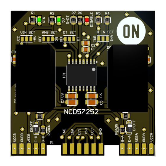
Figure 1. Evaluation Board TOP View
Features
(continued)
•
PCB layout optimized for power supply
bypassing capacitor, gate−driver loop
•
Allows quick verification of most of the
data sheet parameters
1
www.onsemi.com
Publication Order Number:
EVBUM2730/D
Advertisement

Subscribe to Our Youtube Channel
Related Manuals for ON Semiconductor NCD57252


Summary of Contents for ON Semiconductor NCD57252
- Page 1 The NCD57252 Evaluation driver board is designed for evaluation www.onsemi.com of the NCD57252. The NCD57252 is a high current two channel gate driver. It can directly drive two independent IGBTs in any configuration. EVAL BOARD USER’S MANUAL The driver provides 5 kVrms internal galvanic isolation from input to each output and functional isolation between the two output channels.
-
Page 2: Table Of Contents
7, 8 Emitter connection of B channel – connected to GNDB G−B 9, 10 Gate connection of B channel ON−BOARD Jumpers Functional Table Table 2. NCD57252 JUMPERS FUNCTIONAL TABLE Jumper Name Setup Description VIN SET OPEN When using external power supplies for VCCA / VCCB Power supplies need to be connected to the VCCA, VCCB pins on P1 When using DC−DC converter powered by the same voltage as the primary side of the driver... -
Page 3: Gnd
NCD57252GEVB Electrical Specification Table 3. NCD57252 ELECTRICAL SPECIFICATION Description Unit VCCA/VCCB Output positive bias power supply (VCC−VEE max) − Output negative bias power supply − −20 GNDA / GNDB Output bias ground – connected to the IGBT emitter − −... - Page 4 NCD57252GEVB FUNCTIONAL DESCRIPTION Power Supply (VCC, +5V, VCCA, VCCB) • NCD57252 is designed to support unipolar power supply External power supply on both individual channels. The evaluation driver board is designed to support bipolar The evaluation driver board supports two types of output...
- Page 5 Signal Inputs (INA, INB) • ANB SET should be set to OFF when G−A and G−B are To prevent output pulse trimming, NCD57252 is controlled individually by INA and INB (along with equipped by resettable input functionality. DISABLE and DT).
-
Page 6: Vcca
Bench Test Setup This section provides details how to configure the The bench test setup shows the equipment connections. NCD57252 Evaluation board. Basic laboratory equipment Use basic setup procedure as a reference: will be required to perform the tests. •... - Page 7 NCD57252GEVB Test 1 – Typical Performance Waveforms – Propagation Delay To set the board, use this setup as a reference. Make sure the power supplies & outputs of signal generators are powered off / disabled channel 1. VIN SET a. For powering outputs by using external power supplies − open jumper b.
- Page 8 NCD57252GEVB (Legend: C1 – Input A (INA), C2 – Output A (G−A), C3 – Input B (INB), C4 – Output B (G−B)) Figure 7. INPUT and OUTPUT Fall Propagation Delay Waveforms www.onsemi.com...
- Page 9 NCD57252GEVB Test 2 – Typical Performance Waveforms – Independent 2 Channels Driver The NCD57252 can work as 2 independent channel driver. To set the board as 2 independent channel driver, use this setup as a reference. Make sure the power supplies & outputs of signal generators are powered off / disabled channel 1.
- Page 10 NCD57252GEVB (Legend: C1 – Input A (INA), C2 – Output A (G−A), C3 – Input B (INB), C4 – Output B (G−B)) (Input signals from the external signal generator are complementary) Figure 9. INPUT and OUTPUT Signals www.onsemi.com...
- Page 11 Test 3 – Typical Performance Waveforms –2 Channels Complementary Driver without Added Dead Time The NCD57252 can work as 2 channel complementary driver with single channel input without affecting the dead time. To set the board as 2 channel driver, use this setup as a reference.
- Page 12 NCD57252GEVB (Legend: C1 – Input A (INA), C2 – Output A (G−A), C3 – Input B (INB), C4 – Output B (G−B)) Figure 11. INPUT and OUTPUT Signals www.onsemi.com...
- Page 13 Test 4 – Typical Performance Waveforms –2 Channels Complementary Driver with Adjustable Dead Time The NCD57252 can work as 2 channel complementary driver with single channel input with adjustable dead time. To set the board as 2 channel driver, use this setup as a reference.
- Page 14 NCD57252GEVB (Legend: C1 – Input A (INA), C2 – Output A (G−A), C3 – Input B (INB), C4 – Output B (G−B)) Figure 13. INPUT and OUTPUT Signals www.onsemi.com...
- Page 15 NCD57252GEVB SCHEMATIC & LAYOUT DIAGRAMS Schematic Diagram Figure 14. Schematic www.onsemi.com...
- Page 16 NCD57252GEVB Layout Diagrams Figure 15. Assembled PCB TOP View Figure 16. TOP Overlay www.onsemi.com...
- Page 17 NCD57252GEVB Figure 17. Top Layer Figure 18. BOT Layer www.onsemi.com...
- Page 18 NCD57252GEVB Figure 19. BOT Overlay Figure 20. Assembled PCB BOT View www.onsemi.com...
- Page 19 NCD57252GEVB Table 4. BILL OF MATERIAL Quantity Assembled Designator Value Description Package Manufacturer NCD57252 IGBT Driver SOIC−16W ON Semiconductor DAOFF, DBOFF MMSD301T1G Schottky diode 30 V SOD−123 ON Semiconductor VIN, +5V, POWERA, LED SMD GREEN SMD 0805 POWERB DISABLE LED SMD...
- Page 20 onsemi, , and other names, marks, and brands are registered and/or common law trademarks of Semiconductor Components Industries, LLC dba “onsemi” or its affiliates and/or subsidiaries in the United States and/or other countries. onsemi owns the rights to a number of patents, trademarks, copyrights, trade secrets, and other intellectual property. A listing of onsemi’s product/patent coverage may be accessed at www.onsemi.com/site/pdf/Patent−Marking.pdf.
Need help?
Do you have a question about the NCD57252 and is the answer not in the manual?
Questions and answers