Advertisement
Quick Links
NCP51820GAN1GEVB
NCP51820 HB GaN Driver
Evaluation Board
User's Manual
NCP51820 High−Speed, Half−Bridge, GaN
Driver Evaluation Board for Existing or
New PCB Designs
INTRODUCTION
Purpose
The NCP51820 HB GaN Driver Evaluation Board (EVB) is
intended to replace the driver and power MOSFETs used in existing
half−bridge or full−bridge power supplies. This EVB highlights the
performance, simplicity and minimal number of components required
to efficiently and reliably drive two gallium nitride power switches
used in a high−voltage, totem pole configuration. Intended
applications include off−line power converter topologies such as:
LLC, phase−shifted full−bridge, totem pole PFC, active clamp flyback
and forward, dual active−bridge, Phi−2 and high voltage synchronous
buck. This document describes the NCP51820 HB GaN Driver EVB
mated to a 400 V to 12.5 V LLC converter, as one commonly used
example from the topologies listed.
NCP51820 GaN Driver Description
The NCP51820 high−speed, gate driver is designed to meet the
stringent requirements of driving enhancement mode (E−mode), high
electron mobility transistor (HEMT) and gate injection transistor
(GIT) HEMT, gallium nitride (GaN) power switches in off−line,
half−bridge power topologies. The NCP51820 offers short and
matched propagation delays with advanced level shift technology
providing −3.5 V to +650 V (typical) common mode voltage range for
the high−side drive and −3.5 V to +3.5 V common mode voltage range
for the low−side drive. In addition, the device provides stable and
reliable operation when used in high dV/dt environments up to
200 V/ns. In order to fully protect the gates of the GaN power switches
against excessive voltage, both NCP51820 drive stages employ
separate, dedicated voltage regulators to accurately maintain the
gate−source drive signal amplitude. The circuit offers active clamping
of the driver's bias rails thus protecting against potential gate−source
over−voltage under various operating conditions.
The NCP51820 offers important protection functions such as
independent under−voltage lockout (UVLO), monitoring VDD bias
voltage, VDDH and VDDL driver bias and thermal shutdown based
on die junction temperature of the device. As shown in Figure 2, the
Schmitt trigger, EN, HIN and LIN inputs are internally pulled LOW to
assure the driver is always in a default 'OFF' state during initial
application of V
bias. Programmable dead−time control is available
DD
by the DT pin and can be configured to prevent or allow
cross−conduction.
© Semiconductor Components Industries, LLC, 2019
September, 2019 − Rev. 2
EVAL BOARD USER'S MANUAL
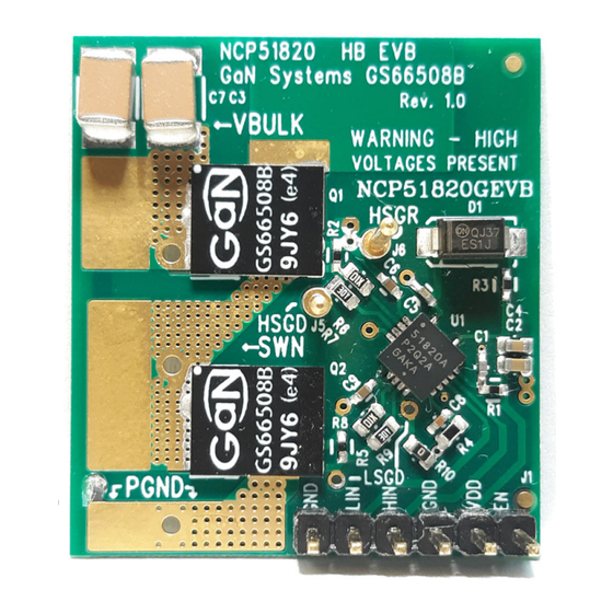
Figure 1. Evaluation Board Photo
1
www.onsemi.com
Publication Order Number:
EVBUM2641/D
Advertisement

Subscribe to Our Youtube Channel
Related Manuals for ON Semiconductor NCP51820GAN1GEVB


Summary of Contents for ON Semiconductor NCP51820GAN1GEVB
- Page 1 NCP51820GAN1GEVB NCP51820 HB GaN Driver Evaluation Board User's Manual NCP51820 High−Speed, Half−Bridge, GaN www.onsemi.com Driver Evaluation Board for Existing or New PCB Designs EVAL BOARD USER’S MANUAL INTRODUCTION Purpose The NCP51820 HB GaN Driver Evaluation Board (EVB) is intended to replace the driver and power MOSFETs used in existing half−bridge or full−bridge power supplies.
- Page 2 NCP51820GAN1GEVB The NCP51820 can be considered as having two includes dedicated input level shifting to ensure accurately independent high−side and low−side “floating” drive stages. matched propagation delays to within 5 ns. Each output The high−side can float up to 650 V referenced to SW and includes separate source and sink allowing rise and fall times the low−side can float up to 3.5 V referenced to PGND,...
- Page 3 NCP51820GAN1GEVB LS Probe GND Figure 3. NCP51820 HB GaN Driver EVB Figure 4. Tip−and−Barrel Measurement Method www.onsemi.com...
- Page 4 NCP51820GAN1GEVB NCP51820 EVB Schematic Figure 5. NCP51820 EVB Schematic www.onsemi.com...
- Page 5 NCP51820GAN1GEVB NCP51820 EVB Bill of Materials (BOM) Table 1. NCP51820 EVB BILL OF MATERIALS Item Reference Value Part Number Description Manufacturer Pkg Type 10 pF CC0402JRNPO9BN100 CAP, SMD, CERAMIC, Yageo 50 V, NPO 1 mF CL10B105KA8NNNC CAP, SMD, CERAMIC, Samsung...
- Page 6 NCP51820GAN1GEVB NCP51820 Layers • • Top Layer: All EVB components are on the top layer. Layer 3 (Internal): Layer 3 has additional high current The large copper high current carrying etches used to carrying etches for the HS/LS GaN power switches.
- Page 7 NCP51820GAN1GEVB NCP51820 EVB I/C Connections Power Stage Input Connector Figure 7. EVB I/O Connections Table 2. I/O CONNECTOR DESCRIPTION Pin Name Pin Type Description Value EN (Note 3) J1−1 Logic input for enabling/disabling the driver 2.5 V < EN < V + 0.3 V...
- Page 8 NCP51820GAN1GEVB NCP51820 EVB CONNECTION METHODS There are two different methods for connecting the EVB Preparing Power Board for EVB Connection 1. Remove HS and LS MOSFETs and HS and LS gate to an existing power board. drive resistors from the power board as illustrated in Power topologies not using a current sense resistor Figure 8.
- Page 9 NCP51820GAN1GEVB Figure 9. Connection Method #1 − No LS Current Sense Resistor Figure 10. Connection Method #2 − LS Current Sense Resistor on Power Board www.onsemi.com...
- Page 10 NCP51820GAN1GEVB External VDD An external VDD can be used, as long as the HIN and LIN 60 V, 1A minimum diode) in series with VDD + to protect signals still fall within the parameters listed in Table 2. If an the VDD supply.
- Page 11 NCP51820GAN1GEVB CONFIGURING ENABLE (EN) AND DEAD−TIME (DT) EN Function and External Control dead−time, anti−cross−conduction protection is The NCP51820 GaN Driver EN is internally pulled low enabled. If HIN and LIN are overlapping by X ns, to SGND, so the driver is always defaulted to a disabled then X ns of dead−time is automatically inserted.
- Page 12 NCP51820GAN1GEVB EN Bypass Capacitor EN Register DT Bypass Capacitor DT Register SGND = PGND Resistor Figure 13. EN and DT Resistor and Capacitor Locations www.onsemi.com...
- Page 13 The NCP51820 HB GaN Driver EVB was mated to an offers best in class efficiency for isolated DC/DC LLC Resonant 250 W, 400 V to 12.5 V converter featuring converters. ON Semiconductor’s FAN7688, a secondary−side LLC Figure 14. FAN7688 LLC with NCP51820 HB GaN Driver EVB Installed www.onsemi.com...
- Page 14 NCP51820GAN1GEVB Figure 15. FAN7688 LLC with NCP51820 HB GaN Driver EVB Installed As shown in Figure 14 and Figure 15, the NCP51820 HB Test Conditions The FAN7688/NCP51820 HB GaN Driver EVB was GaN Driver EVB is being used to replace the MOSFETs and powered up using a 12 V bias for VDD, a high−voltage DC...
- Page 15 NCP51820GAN1GEVB Figure 16. FAN7688 LLC/NCP51820 HB GaN Driver EVB, 380 VIN, 100 kHz, 12.5 V, 20 A Figure 17. FAN7688 LLC/NCP51820 HB GaN Driver EVB, 400 VIN, 100 kHz, 12.5 V, 20 A www.onsemi.com...
- Page 16 NCP51820GAN1GEVB Figure 18. Thermal Image: FAN7688 LLC/NCP51820 HB GaN Driver EVB, 400 VIN, 100 kHz, 12.5 V, 20 A Figure 18 shows a thermal image of EVB operating at density) will not be realized at the lower frequencies that Si 400 V in, 100 kHz, 12.5 V, 20 A out.
- Page 17 LIMITATIONS OF LIABILITY: ON Semiconductor shall not be liable for any special, consequential, incidental, indirect or punitive damages, including, but not limited to the costs of requalification, delay, loss of profits or goodwill, arising out of or in connection with the board, even if ON Semiconductor is advised of the possibility of such damages. In no event shall ON Semiconductor’s aggregate liability from any obligation arising out of or in connection with the board, under any theory of liability, exceed the purchase price paid for the board, if any.
Need help?
Do you have a question about the NCP51820GAN1GEVB and is the answer not in the manual?
Questions and answers