Advertisement
Quick Links
NCV91300 Evaluation Kit
User Manual
EVBUM2789
DOCUMENT DESCRIPTION
Goal of Document
This document describes the operation and use of the NCV91300
evaluation kit. This kit is provided by ON Semiconductor to help user
to evaluate and set up the NCV91300 numerous operation modes as
well as the typical operating characteristics.
In this document, user will find information about hardware and
Graphical User Interface software, as well as typical Bill of Material,
board schematic and layout.
Applicable and Reference Documents
APPLICATION INFORMATION
Supply Input
AVIN
4.7 mF
AGND
Enable Control
EN
Input
AGND
SCL
2
I
C BUS
AGND
SDA
External Clock SYNC
PG
Power Good
INTB
Interrupt
NCV91300 Data Sheet
© Semiconductor Components Industries, LLC, 2021
March, 2021 − Rev. 0
NCV91300
Core
DCDC
3.0 A
Thermal
Protection
Modular
Driver
Enabling
2
Test / I
C
Clocking
Output
DCDC
Monitoring
2.15 MHz
Controller
Interrupt
Figure 1. Typical Application Schematic
EVAL BOARD USER'S MANUAL
PVIN
BOOT
10 nF
SW
PGND
FB
Sense
1
www.onsemi.com
Power Supply Input
10 mF
1.0 mH
10 mF
Processor
Core
Publication Order Number:
EVBUM2789/D
Advertisement

Subscribe to Our Youtube Channel
Related Manuals for ON Semiconductor NCV91300


Summary of Contents for ON Semiconductor NCV91300
- Page 1 Goal of Document www.onsemi.com This document describes the operation and use of the NCV91300 evaluation kit. This kit is provided by ON Semiconductor to help user EVAL BOARD USER’S MANUAL to evaluate and set up the NCV91300 numerous operation modes as well as the typical operating characteristics.
- Page 2 PC to PWM transitions improve overall solution efficiency. The Graphical User Interface software. NCV91300 registers NCV91300 is housed in low profile 3.0 x 3.0 mm QFN−16 are also read through this interface. In that case, the board package.
-
Page 3: Getting Started
EVBUM2789 GETTING STARTED Input / Output Description This section describes the connectors and jumper settings for proper operation as well as the voltage appropriate range. Table 1. EVALUATION BOARD OPERATING RANGE Symbol Parameter Unit Power Supply Range Analog Supply Range Table 2. - Page 4 Evaluation Board is operated cable 1. Install the Graphical User Interface (GUI) 6. Connect NCV91300 Board 2.5 V~5.5 V (See Software on computer table 1) power supply to J3/J8 (J5) and J1/J8 2. Connect the Interface Board to the Board, using...
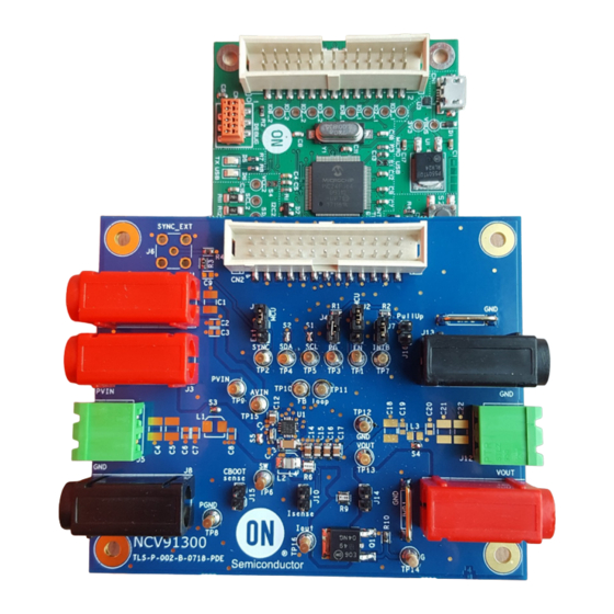
- Page 5 EVBUM2789 Figure 2. Hardware Setup of EVKit (Board To Board Connection) Figure 3. Hardware Setup of EVKit (Ribbon Cable Connection) www.onsemi.com...
-
Page 6: Board Layout
EVBUM2789 BOARD LAYOUT This section includes the SST layer of PCB layout and EVB board pictures. 3 POINTS CONFIGURATION JUMPERS PIN OUT Figure 4. TOP Assembly Figure 5. BOTTOM Assembly www.onsemi.com... - Page 7 EVBUM2789 Figure 6. TOP Figure 7. Inner 1 www.onsemi.com...
- Page 8 EVBUM2789 Figure 8. Inner 2 Figure 9. Bottom www.onsemi.com...
- Page 9 EVBUM2789 J5 Input J12 Output Connector Connector Figure 10. Board Picture TOP View www.onsemi.com...
- Page 10 EVBUM2789 BOARD SCHEMATIC AND BOM This section provides the board schematic as well as standard Bill of Material. Schematic Figure 11. Board Schematic www.onsemi.com...
- Page 11 EVBUM2789 Bill of Material www.onsemi.com...
-
Page 12: Gui Software
GUI SOFTWARE Once hardware is properly installed and set up, user may At start up, the GUI will first read NCV91300 use the Graphical User Interface software (GUI in the rest of configuration. Please make sure that hardware is supplied the document) to set up NCV91300 and read configurations prior to GUI startup. - Page 13 EVBUM2789 You can click on the Generic tab to access to the generic window, where individual register can be addressed Figure 14. Generic Window You can click on the Register tab to access to the Register window, where all register can be read and write Figure 15.
- Page 14 EVBUM2789 NCV91300 CONFIGURATION Table 5. NCV91300 CONFIGURATION 3.5 A 2.5 A NCV91300A NCV91300B Configuration Default I C address ADD1 – 14h : 0010100R/W ADD1 – 14h : 0010100R/W PID product identification RID revision identification Metal Metal FID feature identification Default VOUT 1.25 V...
- Page 15 EVBUM2789 Table 7. I C REGISTERS MAP CONFIGURATION (NCV91300MNWBTXG) Register Name Add. Type Def. Function INT_ACK1 Interrupt register 1 INT_ACK2 Interrupt register 2 INT_SEN1 Sense register 1 (real time status) INT_SEN2 Sense register 2 (real time status) INT_MSK1 Mask register 1 to enable or disable interrupt sources (trim) INT_MSK2 Mask register 2 to enable or disable interrupt sources (trim) Product Identification...
-
Page 16: Registers Description
EVBUM2789 REGISTERS DESCRIPTION The tables below describe the I2C registers. Reserved Address is reserved and register / bit is not physically designed Registers / Bits Operations: Spare Address is reserved and register / bit is Read only register physically designed Write to 1 to Clear In bold default can be factory programmed upon request. - Page 17 EVBUM2789 Table 9. INTERRUPT ACKNOWLEDGE REGISTER 2 Name: INTACK2 Address: 01h Type: W1C Default: 00000000b (00h) Trigger: Dual Edge [D7..D0] Spare = 0 ACK_TSD ACK_TWARN ACK_TPREW Spare = 0 ACK_BUS ACK_CLK ACK_PG Bit Description ACK_PG Power Good Sense Acknowledgement 0: Cleared 1: DC−DC Power Good Event detected ACK_CLK Working Clock Indicator Acknowledgement...
- Page 18 EVBUM2789 Table 11. INTERRUPT SENSE REGISTER 2 Name: INTSEN2 Address: 03h Type: R Default: 00000000b (00h) Trigger: N/A Spare = 0 SEN_TSD SEN_TWARN SEN_TPREW Spare = 0 SEN_BUS SEN_CLK SEN_PG Bit Description SEN_PG Power Good Sense 0: DC−DC Output Voltage below target 1: DC−DC Output Voltage within nominal range SNS_CLK Working Clock Indicator Sense...
- Page 19 EVBUM2789 Table 13. INTERRUPT MASK REGISTER 2 Name: INTMSK2 Address: 05h Type: RW Default: See Register map Trigger: N/A Spare = 1 MSK_TSD MSK_TWARN MSK_TPREW Spare = 1 MSK_BUS MSK_CLK MSK_PG Bit Description MSK_PG Power Good interrupt source mask 0: Interrupt is Enabled 1: Interrupt is Masked MSK_CLK Working Clock Indicator interrupt Mask...
- Page 20 EVBUM2789 Table 16. FEATURE ID REGISTER Name: FID Address: 08h Type: R Default: See Register map Trigger: N/A Spare Spare Spare Spare FID_3 FID_2 FID_1 FID_0 Bit Description FID[3..0] Feature Identification Table 17. DC−DC VOLTAGE PROG REGISTER Name: PROG Address: 09h Type: RW Default: See Register map Trigger: N/A...
- Page 21 EVBUM2789 Table 18. COMMAND Name: COMMAND Address: 0Ah Type: RW Default: See Register map Trigger: N/A DVSMODE SLEEP_MODE DISCHG PGCLK ENABLE PGDVS PGDCDC Bit Description PGDCDC Power Good Enabling 0 = Disabled 1 = Enabled PGDVS Power Good Active On DVS 0 = Disabled 1 = Enabled ENABLE...
- Page 22 01 = 3.5 A (for 2.5 A output current) 10 = 4.0 A (for 3.0 A output current) 11 = 4.5 A (for 3.5 A output current) ON Semiconductor is licensed by the Philips Corporation to carry the I C bus protocol. www.onsemi.com...
- Page 23 onsemi, , and other names, marks, and brands are registered and/or common law trademarks of Semiconductor Components Industries, LLC dba “onsemi” or its affiliates and/or subsidiaries in the United States and/or other countries. onsemi owns the rights to a number of patents, trademarks, copyrights, trade secrets, and other intellectual property. A listing of onsemi’s product/patent coverage may be accessed at www.onsemi.com/site/pdf/Patent−Marking.pdf.
Need help?
Do you have a question about the NCV91300 and is the answer not in the manual?
Questions and answers