Advertisement
Quick Links
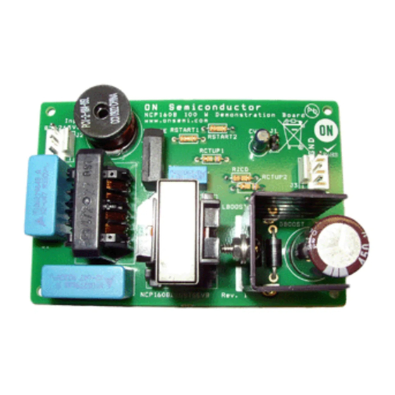
NCP1608BOOSTGEVB
NCP1608 100 W Boost
Evaluation Board User's
Manual
Introduction
The NCP1608 is a voltage mode power factor correction
(PFC) controller designed to implement converters to
comply with line current harmonic regulations. The device
operates in critical conduction mode (CrM) for optimal
performance in applications up to 350 W. Its voltage mode
scheme enables it to obtain near unity power factor (PF)
without the need for a line-sensing network. The output
voltage is accurately controlled with an integrated high
precision transconductance error amplifier. The controller
also implements a comprehensive set of safety features that
simplify system design.
This application note describes the design and
implementation of a 400 V, 100 W, CrM boost PFC
converter using the NCP1608. The converter exhibits high
PF, low standby power dissipation, high active mode
efficiency, and a variety of protection features.
Rectifiers
AC Line
Basic Operation of a CrM Boost Converter
For medium power (< 350 W) applications, CrM is the
preferred control method. CrM operates at the boundary
between discontinuous conduction mode (DCM) and
continuous conduction mode (CCM). In CrM, the drive on
time begins when the inductor current reaches zero.
CrM combines the reduced peak current of CCM
operation with the zero current switching of DCM
© Semiconductor Components Industries, LLC, 2012
November, 2012 − Rev. 1
PFC Pre−Converter
High
+
Frequency
NCP1608
Bypass
Capacitor
Figure 1. Active PFC Stage with the NCP1608
EVAL BOARD USER'S MANUAL
The Need for PFC
Most electronic ballasts and switch−mode power supplies
(SMPS) use a diode bridge rectifier and a bulk storage
capacitor to produce a dc voltage from the utility ac line.
This causes a non-sinusoidal current consumption and
increases the stress on the power delivery infrastructure.
Government regulations and utility requirements mandate
control over line current harmonic content. Active PFC
circuits are the most popular method to comply with these
harmonic content requirements. System solutions consist of
connecting a PFC pre−converter between the rectifier bridge
and the bulk capacitor (Figure 1). The boost converter is the
most popular topology for active PF correction. It produces
a constant output voltage and consumes a sinusoidal input
current from the line.
Bulk
+
Storage
Capacitor
operation. This control method causes the frequency to vary
with the instantaneous line input voltage (V
load. The operation and waveforms of a CrM PFC boost
converter are illustrated in Figure 2. For detailed
information on the operation of a CrM boost converter for
PFC
applications,
please
www.onsemi.com.
1
http://onsemi.com
Converter
) and the output
in
refer
to
AND8123
Publication Order Number:
EVBUM2162/D
Load
at
Advertisement

Subscribe to Our Youtube Channel
Related Manuals for ON Semiconductor NCP1608BOOSTGEVB


Summary of Contents for ON Semiconductor NCP1608BOOSTGEVB
- Page 1 NCP1608BOOSTGEVB NCP1608 100 W Boost Evaluation Board User's Manual http://onsemi.com EVAL BOARD USER’S MANUAL Introduction The NCP1608 is a voltage mode power factor correction (PFC) controller designed to implement converters to The Need for PFC comply with line current harmonic regulations. The device Most electronic ballasts and switch−mode power supplies...
- Page 2 NCP1608BOOSTGEVB Diode Bridge Diode Bridge drain AC Line AC Line drain − − The power switch is ON The power switch is OFF With the power switch voltage being about zero, the The inductor current flows through the diode. The inductor input voltage is applied across the inductor.
- Page 3 The design of a CrM boost PFC converter is discussed in . A resistor in series with the ZCD winding ZCD(TRIG) many ON Semiconductor application notes. Table 1 lists limits the ZCD pin current. some examples. The NCP1608 features a powerful output driver on the This application note describes the design procedure for DRV pin.
- Page 4 NCP1608BOOSTGEVB MOSFET Conduction 2 @ 85 @ 0.92 Diode Conduction @ 1 * + 50.5 kHz SW(LL) 2 @ 460 m @ 100 2 @ 265 @ 0.92 L(peak) @ 1 * + 44.3 kHz SW(HL) 2 @ 460 m @ 100 L(NEG) is equal to 50.5 kHz at Vac...
- Page 5 NCP1608BOOSTGEVB bulk EQ(drain) AC Line Filter Figure 5. Equivalent Drain Capacitance Discharge Path is the combined parasitic capacitances of the EQ(drain) out1 (eq. 8) MOSFET, the diode, and the inductor. C is charged by the out2 * 1 * R energy discharged by C .
- Page 6 NCP1608BOOSTGEVB The value of C is selected as 68 mF to reduce DESIGN STEP 6: Size the Power Components bulk The power components are sized such that there is to less than 15 V. This results in a peak ripple(peak-peak) sufficient margin to sustain the currents and voltages applied output voltage of 406.25 V, which is less than the peak output...
- Page 7 NCP1608BOOSTGEVB Once V reaches V , the internal references and + 0.5 CC(on) + 0.138 W sense 3.62 logic of the NCP1608 turn on. The NCP1608 includes an The current sense resistor is selected as 0.125 W for undervoltage lockout (UVLO) feature that ensures that the decreased power dissipation.
- Page 8 NCP1608BOOSTGEVB bulk PFC(V − NCP1230 NCP1608 Figure 8. Using the SMPS Controller to Supply Power to the NCP1608 DESIGN STEP 8: Limit the Inrush Current bypass The sudden application of the ac line voltage to the PFC pre−converter causes an inrush current and a resonant voltage overshoot that is several times the normal value.
- Page 9 NCP1608BOOSTGEVB The type 2 network is composed of C , and COMP COMP1 (eq. 24) COMP1 2 @ p @ f sets the crossover frequency (f ) and zero COMP1 COMP1 CROSS COMP is calculated using Equation 23: + 19.3 kW COMP1 2 @ p @ 2.5 @ 3.3 m...
- Page 10 NCP1608BOOSTGEVB Vin (100V/div) (500mA/div) (10V/div, ac coupled) Zero Crossing Distortion Figure 13. Full Load Input Current (V = 230 Vac 50 Hz, I = 250 mA) The zero crossing distortion increases the THD and reduces the instantaneous input voltage at which the decreases the PF of the pre-converter.
- Page 11 NCP1608BOOSTGEVB Vac(t) with R CTUP no R CTUP no R CTUP with R CTUP time Figure 15. On Time and Switching Frequency With and Without R CTUP The dependency of THD on R is illustrated in CTUP Figure 16. = open...
- Page 12 NCP1608BOOSTGEVB Control Control switch Driver charge − gate Ct(off) sense (offset) Figure 18. Block Diagram of the Propagation Delay Components There is a delay (t ) from when V is reached to A value of R = 365 W compensates for the propagation...
- Page 13 NCP1608BOOSTGEVB Design Results The completed evaluation board schematic is shown in Figure 22. Figure 22. NCP1608BOOSTGEVB Evaluation Board Schematic The bill of materials (BOM), layout, and summary of − The input power, PF, and THD are measured using a boost equations are shown in Appendix 1, Appendix 2, and PM3000A power meter Appendix 3 respectively.
- Page 14 NCP1608BOOSTGEVB 115 Vac 60 Hz 230 Vac 50 Hz = 50 W = 75 W = 100 W IEC61000−3−2 Class D Limits Vin (Vac) Nth HARMONIC Figure 23. THD vs. Input Voltage Figure 24. Individual Harmonic Current 1.00 0.99 = 100 W 0.98...
- Page 15 NCP1608BOOSTGEVB Input Current and Output Voltage The input current and output voltage ripple are shown in Figure 28. The NCP1608 detects an OVP fault when V Figure 27. The overvoltage protection is observed by reaches 421 V and restarts when V decreases to 410 V.
- Page 16 NCP1608BOOSTGEVB Frequency Response The frequency response is measured at the minimum and crossover frequency is 2 Hz and the phase margin is 71°. maximum input voltages and maximum output power. Figure 30 shows that at maximum input voltage, the Figure 29 shows that at minimum input voltage, the crossover frequency is 10 Hz and the phase margin is 53°.
- Page 17 NCP1608BOOSTGEVB Floating Pin Protection (FPP) Jumper The evaluation board includes a jumper (J1) between the Figure 31. If J1 is removed during operation, the drive is FB pin and the feedback network to demonstrate the FPP disabled as shown in Figure 32. J1 is for FPP evaluation feature of the NCP1608.
- Page 18 NCP1608BOOSTGEVB The evaluation board can be configured for THD reduction or power dissipation reduction. Table 3 shows the configuration results. Table 3. EVALUATION BOARD CONFIGURATION RESULTS Efficiency (P = 100 W) THD (P = 100 W) 115 Vac 230 Vac...
- Page 19 NCP1608BOOSTGEVB Table 4. BILL OF MATERIALS* Substi- Desig- Toler- Manufacturer Part tution nator Description Value ance Footprint Manufacturer Number Allowed BRIDGE Bridge Rectifier, 4 A, 600 V − − Vishay KBL06-E4/51 C1, C2 Capacitor, EMI Suppression, 0.47 mF Radial EPCOS...
- Page 20 NCP1608BOOSTGEVB Table 4. BILL OF MATERIALS* Substi- Desig- Toler- Manufacturer Part tution nator Description Value ance Footprint Manufacturer Number Allowed Thermistor, Inrush Current 4.7 W Radial EPCOS B57238S479M Limiter MOSFET, N−Channel, − − TO−220 Infineon SPP12N50C3 11.6 A, 560 V...
- Page 21 NCP1608BOOSTGEVB LAYOUT Figure 34. Top View of the Layout Figure 35. Bottom View of the Layout http://onsemi.com...
- Page 22 NCP1608BOOSTGEVB TEST PROCEDURE FOR THE NCP1608BOOSTGEVB EVALUATION BOARD Required Equipment 15. Repeat steps 9-13 with the ac source set to 115 Vac (*Equivalent test equipment may be substituted.) / 60 Hz, 230 Vac / 50 Hz, 265 Vac / 50 Hz. Verify •...
- Page 23 NCP1608BOOSTGEVB Figure 36. Test Setup http://onsemi.com...
- Page 24 NCP1608BOOSTGEVB Table 6. SUMMARY OF BOOST EQUATIONS Components are identified in Figure 3 Input rms Current h (the efficiency of only the PFC stage) is generally in the range of 90 Iac + − 95%. Vac is the rms ac line input h @ Vac voltage.
- Page 25 PUBLICATION ORDERING INFORMATION LITERATURE FULFILLMENT: N. American Technical Support: 800−282−9855 Toll Free ON Semiconductor Website: www.onsemi.com Literature Distribution Center for ON Semiconductor USA/Canada Order Literature: http://www.onsemi.com/orderlit P.O. Box 5163, Denver, Colorado 80217 USA Europe, Middle East and Africa Technical Support: Phone: 303−675−2175 or 800−344−3860 Toll Free USA/Canada...
Need help?
Do you have a question about the NCP1608BOOSTGEVB and is the answer not in the manual?
Questions and answers