Table of Contents
Advertisement
Quick Links
www.ti.com
User's Guide
Using the UCC14131EVM-070 for Biasing GaN and Gate
Driver ICs in Automotive and Industrial Applications
This user's guide provides a description and instructions for use of the UCC14131EVM-070 to evaluate the
UCC14131-Q1; a high frequency, integrated transformer, DC-DC converter module from Texas Instruments. This
EVM allows designers to quickly and efficiently evaluate the UCC14131-Q1 for use in automotive or industrial
applications requiring gate driver IC bias power as high as 1.5 W, meeting up to 5 kV
1
Introduction.............................................................................................................................................................................3
1.1 Pin Configuration and Functions........................................................................................................................................
2 Description..............................................................................................................................................................................
2.1 EVM Electrical Performance Specifications.......................................................................................................................
3
Schematic................................................................................................................................................................................7
Operation......................................................................................................................................................8
4.1 Recommended Test Equipment.........................................................................................................................................
4.2 External Connections for Easy Evaluation.........................................................................................................................
4.3 Powering the EVM.............................................................................................................................................................
Points.................................................................................................................................................................9
4.5 Probing the EVM..............................................................................................................................................................
5 Performance Data.................................................................................................................................................................
5.1 Efficiency Data.................................................................................................................................................................
5.2 Regulation Data...............................................................................................................................................................
Current...............................................................................................................................................15
Waveforms.........................................................................................................................................................15
5.5 Inrush Current..................................................................................................................................................................
5.6 AC Ripple Voltage............................................................................................................................................................
Timing..................................................................................................................................................................22
5.8
RLIM.................................................................................................................................................................................22
5.9 Shutdown.........................................................................................................................................................................
5.10 Thermal Performance....................................................................................................................................................
(BOM)..........................................................................................................................................................30
Figure 2-2. UCC14141EVM-070 (Bottom View)..........................................................................................................................
Figure 3-1. UCC14131EVM-070 Schematic Diagram.................................................................................................................
Figure 4-2. UCC14131EVM-070, PCB Scope Probe Test Points..............................................................................................
Figure 5-2. Regulation vs Power, VDD-VEE Loading Only.......................................................................................................
Figure 5-3. Regulation vs Current, VDD-VEE Loading Only.....................................................................................................
SLUUCU2 - MARCH 2023
Submit Document Feedback
ABSTRACT
Table of Contents
Layers...........................................................................................................26
List of Figures
View)..................................................................................................................3
View)................................................................................................................................5
Setup......................................................................................................................8
Only.............................................................................................12
Only....................................................................................................15
= 0 mA..................................................................................................
= 0 mA..............................................................................................
= 10 mA................................................................................................
= 10 mA............................................................................................
Copyright © 2023 Texas Instruments Incorporated
Using the UCC14131EVM-070 for Biasing GaN and Gate Driver ICs in
Automotive and Industrial Applications
Table of Contents
isolation.
RMS
3
5
6
8
8
9
11
12
12
14
18
20
24
25
5
7
11
14
14
15
16
16
17
1
Advertisement
Table of Contents

Subscribe to Our Youtube Channel
Related Manuals for Texas Instruments UCC14131EVM-070


Summary of Contents for Texas Instruments UCC14131EVM-070
-
Page 1: Table Of Contents
Driver ICs in Automotive and Industrial Applications ABSTRACT This user’s guide provides a description and instructions for use of the UCC14131EVM-070 to evaluate the UCC14131-Q1; a high frequency, integrated transformer, DC-DC converter module from Texas Instruments. This EVM allows designers to quickly and efficiently evaluate the UCC14131-Q1 for use in automotive or industrial applications requiring gate driver IC bias power as high as 1.5 W, meeting up to 5 kV... - Page 2 ..........................13 Table 7-1. UCC14131EVM-070 BOM............................Trademarks All trademarks are the property of their respective owners. Using the UCC14131EVM-070 for Biasing GaN and Gate Driver ICs in SLUUCU2 – MARCH 2023 Automotive and Industrial Applications Submit Document Feedback Copyright © 2023 Texas Instruments Incorporated...
-
Page 3: Introduction
GNDP GNDP GNDP GNDP Figure 1-1. DWN Package, 36-Pin SSOP (Top View) SLUUCU2 – MARCH 2023 Using the UCC14131EVM-070 for Biasing GaN and Gate Driver ICs in Submit Document Feedback Automotive and Industrial Applications Copyright © 2023 Texas Instruments Incorporated... -
Page 4: Table 1-1. Pin Functions (Refer And Follow The Data Sheet)
VEEA pin. P = power, G = ground, I = input, O = output Using the UCC14131EVM-070 for Biasing GaN and Gate Driver ICs in SLUUCU2 – MARCH 2023 Automotive and Industrial Applications Submit Document Feedback Copyright ©... -
Page 5: Description
Description 2 Description The UCC14131EVM-070 is intended to allow designers to evaluate the performance characteristics and capabilities of the UCC14131-Q1 quickly and easily for use in automotive, isolated, gate driver bias applications, as well as a variety of isolated industrial bias power applications. The EVM allows users to test functions of the UCC14131-Q1 such as: Enable/Disable (EN) of the device and easily apply variable loads to the outputs. -
Page 6: Evm Electrical Performance Specifications
[+5V] °C above ambient Switching frequency is specified as primary-side switching frequency. Secondary-side is 2x primary. Using the UCC14131EVM-070 for Biasing GaN and Gate Driver ICs in SLUUCU2 – MARCH 2023 Automotive and Industrial Applications Submit Document Feedback Copyright © 2023 Texas Instruments Incorporated... -
Page 7: Schematic
X on the secondary side, placed directly over the component. Figure 3-1. UCC14131EVM-070 Schematic Diagram SLUUCU2 – MARCH 2023 Using the UCC14131EVM-070 for Biasing GaN and Gate Driver ICs in Submit Document Feedback Automotive and Industrial Applications Copyright © 2023 Texas Instruments Incorporated... -
Page 8: Evm Setup And Operation
Thermal camera (optional) or thermocouple to measure U1 case temperature 4.2 External Connections for Easy Evaluation The UCC14131EVM-070 EVM utilizes screw terminals for quickly connecting to VIN, VDD, [+5V] and VEE (refer Table 4-1). Connecting the appropriate ammeters and voltmeters, as shown in... -
Page 9: Powering The Evm
Figure 4-1 to locate test point location on the board for TP1, TP2, etc. SLUUCU2 – MARCH 2023 Using the UCC14131EVM-070 for Biasing GaN and Gate Driver ICs in Submit Document Feedback Automotive and Industrial Applications Copyright © 2023 Texas Instruments Incorporated... -
Page 10: Table 4-1. Input, Output, Test Point (I/O/Tp)
GNDP, shared primary GND test point TP11 GNDP Black GNDP, shared primary GND test point Using the UCC14131EVM-070 for Biasing GaN and Gate Driver ICs in SLUUCU2 – MARCH 2023 Automotive and Industrial Applications Submit Document Feedback Copyright © 2023 Texas Instruments Incorporated... -
Page 11: Probing The Evm
[+5V](TP3) and [+12V](TP6), which are referenced to VEE or GNDS. SLUUCU2 – MARCH 2023 Using the UCC14131EVM-070 for Biasing GaN and Gate Driver ICs in Submit Document Feedback Automotive and Industrial Applications... -
Page 12: Performance Data
Note VDD, VEE, and [+5V], etc., refer to Table 4-1 Figure 4-1. Using the UCC14131EVM-070 for Biasing GaN and Gate Driver ICs in SLUUCU2 – MARCH 2023 Automotive and Industrial Applications Submit Document Feedback Copyright © 2023 Texas Instruments Incorporated... -
Page 13: Table 5-2. Efficiency Test Data (Vin = 12 V)
Note VDD, VEE, and [+5V], etc., refer to Table 4-1 Figure 4-1. SLUUCU2 – MARCH 2023 Using the UCC14131EVM-070 for Biasing GaN and Gate Driver ICs in Submit Document Feedback Automotive and Industrial Applications Copyright © 2023 Texas Instruments Incorporated... -
Page 14: Regulation Data
VIN = 14 V 11.2 (mA) VDD-VEE Figure 5-3. Regulation vs Current, VDD-VEE Loading Only Using the UCC14131EVM-070 for Biasing GaN and Gate Driver ICs in SLUUCU2 – MARCH 2023 Automotive and Industrial Applications Submit Document Feedback Copyright © 2023 Texas Instruments Incorporated... -
Page 15: Steady State Input Current
Note VDD, VEE, and [+5V], etc., refer to Table 4-1 Figure 4-1. SLUUCU2 – MARCH 2023 Using the UCC14131EVM-070 for Biasing GaN and Gate Driver ICs in Submit Document Feedback Automotive and Industrial Applications Copyright © 2023 Texas Instruments Incorporated... -
Page 16: Figure 5-6. Start-Up 2: Vin = 12 V, Ivdd = 130 Ma, I [+5V] = 0 Ma
Note VDD, VEE, and [+5V], etc., refer to Table 4-1 Figure 4-1. Using the UCC14131EVM-070 for Biasing GaN and Gate Driver ICs in SLUUCU2 – MARCH 2023 Automotive and Industrial Applications Submit Document Feedback Copyright © 2023 Texas Instruments Incorporated... -
Page 17: Figure 5-8. Start-Up 4: Vin = 12 V, Ivdd = 130 Ma, I [+5V] = 10 Ma
Figure 5-8. Start-up 4: VIN = 12 V, I = 130 mA, I = 10 mA [+5V] SLUUCU2 – MARCH 2023 Using the UCC14131EVM-070 for Biasing GaN and Gate Driver ICs in Submit Document Feedback Automotive and Industrial Applications Copyright © 2023 Texas Instruments Incorporated... -
Page 18: Inrush Current
Figure 5-10. Inrush Current: VIN = 12 V, I = 130 mA, I = 10 mA [+5V] Using the UCC14131EVM-070 for Biasing GaN and Gate Driver ICs in SLUUCU2 – MARCH 2023 Automotive and Industrial Applications Submit Document Feedback Copyright © 2023 Texas Instruments Incorporated... -
Page 19: Figure 5-11. Inrush Current: Vin = 12 V, Ivdd = 0 Ma, I [+5V] = 0 Ma
Figure 5-12. Inrush Current: VIN = 12 V, I = 0 mA, I = 0 mA [+5V] SLUUCU2 – MARCH 2023 Using the UCC14131EVM-070 for Biasing GaN and Gate Driver ICs in Submit Document Feedback Automotive and Industrial Applications Copyright © 2023 Texas Instruments Incorporated... -
Page 20: Ac Ripple Voltage
Figure 5-14. AC Ripple: VIN = 12 V, I = 130 mA, I = 10 mA [+5V] Using the UCC14131EVM-070 for Biasing GaN and Gate Driver ICs in SLUUCU2 – MARCH 2023 Automotive and Industrial Applications Submit Document Feedback Copyright © 2023 Texas Instruments Incorporated... -
Page 21: Figure 5-15. Ac Ripple: Vin = 12 V, Ivdd =0 Ma, I [+5V] = 0 Ma
Figure 5-16. AC Ripple: VIN = 12 V, I = 130 mA, I = 10 mA [+5V] SLUUCU2 – MARCH 2023 Using the UCC14131EVM-070 for Biasing GaN and Gate Driver ICs in Submit Document Feedback Automotive and Industrial Applications Copyright © 2023 Texas Instruments Incorporated... -
Page 22: And Timing
Note VDD, VEE, and [+5V], etc., refer to Table 4-1 Figure 4-1. Using the UCC14131EVM-070 for Biasing GaN and Gate Driver ICs in SLUUCU2 – MARCH 2023 Automotive and Industrial Applications Submit Document Feedback Copyright © 2023 Texas Instruments Incorporated... -
Page 23: Figure 5-20. Rlim: Vin = 12 V, Ivdd = 130 Ma, I [+5V] = 10 Ma
Figure 5-20. RLIM: VIN = 12 V, I = 130 mA, I = 10 mA [+5V] SLUUCU2 – MARCH 2023 Using the UCC14131EVM-070 for Biasing GaN and Gate Driver ICs in Submit Document Feedback Automotive and Industrial Applications Copyright © 2023 Texas Instruments Incorporated... -
Page 24: Shutdown
Figure 5-22. Shutdown by EN Low: VIN = 12 V, I = 130 mA, I = 10 mA [+5V] Using the UCC14131EVM-070 for Biasing GaN and Gate Driver ICs in SLUUCU2 – MARCH 2023 Automotive and Industrial Applications Submit Document Feedback... -
Page 25: Thermal Performance
Figure 5-25. VIN=12 V, I =0 mA, POUT=0 W = 30.5°C − 23.9°C = 6.6°C RISE SLUUCU2 – MARCH 2023 Using the UCC14131EVM-070 for Biasing GaN and Gate Driver ICs in Submit Document Feedback Automotive and Industrial Applications Copyright © 2023 Texas Instruments Incorporated... -
Page 26: Assembly And Printed Circuit Board (Pcb) Layers
6 Assembly and Printed Circuit Board (PCB) Layers The UCC14131EVM-070 is designed using a four-layer, FR4, PCB, fabricated with 2-ounce copper on all four layers. The EVM, PCB demonstrates the important use of ground planes and tented stitching vias for shielding and improving EMI performance. -
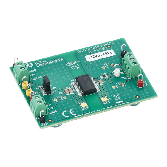
Page 27: Figure 6-3. Ucc14131Evm-070, 3D Angle View
Figure 6-3. UCC14131EVM-070, 3D Angle View Figure 6-4. UCC14131EVM-070, PCB Top Layer, Assembly SLUUCU2 – MARCH 2023 Using the UCC14131EVM-070 for Biasing GaN and Gate Driver ICs in Submit Document Feedback Automotive and Industrial Applications Copyright © 2023 Texas Instruments Incorporated... -
Page 28: Figure 6-5. Ucc14131Evm-070, Gnd Layer 2 (Same As Layer 3)
Figure 6-5. UCC14131EVM-070, GND Layer 2 (same as layer 3) Figure 6-6. UCC14131EVM-070, GND Layer 3 (same as layer 2) Using the UCC14131EVM-070 for Biasing GaN and Gate Driver ICs in SLUUCU2 – MARCH 2023 Automotive and Industrial Applications Submit Document Feedback Copyright ©... -
Page 29: Figure 6-7. Ucc14131Evm-070, Pcb Bottom Layer, Assembly (Mirrored View)
Assembly and Printed Circuit Board (PCB) Layers Figure 6-7. UCC14131EVM-070, PCB Bottom Layer, Assembly (mirrored view) SLUUCU2 – MARCH 2023 Using the UCC14131EVM-070 for Biasing GaN and Gate Driver ICs in Submit Document Feedback Automotive and Industrial Applications Copyright © 2023 Texas Instruments Incorporated... -
Page 30: Bill Of Materials (Bom)
1.5W, 12V-Vin, 12V-Vout, High-Density, 5 UCC14131DWNQ1 Texas Instruments kVRMS Isolated DC-DC Module Using the UCC14131EVM-070 for Biasing GaN and Gate Driver ICs in SLUUCU2 – MARCH 2023 Automotive and Industrial Applications Submit Document Feedback Copyright © 2023 Texas Instruments Incorporated... - Page 31 STANDARD TERMS FOR EVALUATION MODULES Delivery: TI delivers TI evaluation boards, kits, or modules, including any accompanying demonstration software, components, and/or documentation which may be provided together or separately (collectively, an “EVM” or “EVMs”) to the User (“User”) in accordance with the terms set forth herein.
- Page 32 www.ti.com Regulatory Notices: 3.1 United States 3.1.1 Notice applicable to EVMs not FCC-Approved: FCC NOTICE: This kit is designed to allow product developers to evaluate electronic components, circuitry, or software associated with the kit to determine whether to incorporate such items in a finished product and software developers to write software applications for use with the end product.
- Page 33 www.ti.com Concernant les EVMs avec antennes détachables Conformément à la réglementation d'Industrie Canada, le présent émetteur radio peut fonctionner avec une antenne d'un type et d'un gain maximal (ou inférieur) approuvé pour l'émetteur par Industrie Canada. Dans le but de réduire les risques de brouillage radioélectrique à...
- Page 34 www.ti.com EVM Use Restrictions and Warnings: 4.1 EVMS ARE NOT FOR USE IN FUNCTIONAL SAFETY AND/OR SAFETY CRITICAL EVALUATIONS, INCLUDING BUT NOT LIMITED TO EVALUATIONS OF LIFE SUPPORT APPLICATIONS. 4.2 User must read and apply the user guide and other available documentation provided by TI regarding the EVM prior to handling or using the EVM, including without limitation any warning or restriction notices.
- Page 35 Notwithstanding the foregoing, any judgment may be enforced in any United States or foreign court, and TI may seek injunctive relief in any United States or foreign court. Mailing Address: Texas Instruments, Post Office Box 655303, Dallas, Texas 75265 Copyright © 2023, Texas Instruments Incorporated...
- Page 36 TI products. TI’s provision of these resources does not expand or otherwise alter TI’s applicable warranties or warranty disclaimers for TI products. TI objects to and rejects any additional or different terms you may have proposed. IMPORTANT NOTICE Mailing Address: Texas Instruments, Post Office Box 655303, Dallas, Texas 75265 Copyright © 2023, Texas Instruments Incorporated...
Need help?
Do you have a question about the UCC14131EVM-070 and is the answer not in the manual?
Questions and answers