Table of Contents
Advertisement
Quick Links
www.ti.com
EVM User's Guide: UCC21551CQEVM-079
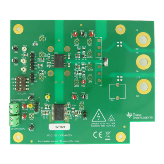
UCC21551CQEVM-079 Evaluation Module
Description
The UCC21551CQEVM-079 is a two copper layer
PCB containing multiple test points and jumpers
to fully evaluate the functionality of the UCC21551
gate driver. The EVM features PWM input control,
onboard adjustable power supply, sockets for discrete
FETs, external active clamp for low side protection,
bootstrapped high side power supply, negative gate
voltage capability, configurable deadtime switches,
EN/DIS jumpers, and socket for Wolfspeed XM3 SiC-
based half bridge power modules. The layout has
been optimized to minimize gate loop area for each
channel and placement of bypass capacitors allow for
SLUUCT9 – SEPTEMBER 2023
Submit Document Feedback
clean and sharp signal reading with minimal noise
interference.
Features
•
Variety of test points to help evaluate all of the gate
driver functions
•
Onboard isolated adjustable bias supply
configured for 20 V
•
Selectable dead time modes: overlap, interlock,
programmable
•
Low side external active clamping circuit
•
16 V/-3V Zener negative voltage pulldown circuit
for SiC FETs
•
Socket for Wolfspeed XM3 module
PCB Top Side
Copyright © 2023 Texas Instruments Incorporated
UCC21551CQEVM-079 Evaluation Module
Description
1
Advertisement
Table of Contents

Subscribe to Our Youtube Channel
Related Manuals for Texas Instruments UCC21551CQEVM-079


Summary of Contents for Texas Instruments UCC21551CQEVM-079
- Page 1 EVM User's Guide: UCC21551CQEVM-079 UCC21551CQEVM-079 Evaluation Module clean and sharp signal reading with minimal noise Description interference. The UCC21551CQEVM-079 is a two copper layer Features PCB containing multiple test points and jumpers to fully evaluate the functionality of the UCC21551 •...
-
Page 2: Kit Contents
UCC21551CQEVM-079 two layer PCB 1.3 Specification UCC21551CQEVM-079 primary function is to evaluate the UCC2155xx dual channel gate driver family. Multiple test points enable monitoring of the different input and outputs of the gate driver for thorough performance evaluation. The gate driver output can be configured to drive a capacitive loads for low voltage testing as well as discrete MOSFETs in a halfbridge configuration. - Page 3 EVM in an adequate lucent plastic box with interlocks from accidental touch. • Limitation for Safe Use: – EVMs are not to be used as all or part of a production unit. SLUUCT9 – SEPTEMBER 2023 UCC21551CQEVM-079 Evaluation Module Submit Document Feedback Copyright © 2023 Texas Instruments Incorporated...
- Page 4 High Voltage! Electric shock is possible when connecting board to live wire. Board must be handled with care by a professional. For safety, use of isolated test equipment with overvoltage and overcurrent protection is highly recommended. UCC21551CQEVM-079 Evaluation Module SLUUCT9 – SEPTEMBER 2023 Submit Document Feedback Copyright © 2023 Texas Instruments Incorporated...
-
Page 5: Header Information
Hardware 2 Hardware 2.1 Power Requirements Table 2-1. UCC21551CQEVM-079 Electrical Specifications Description Units Enable for UCC21551 and UCC14240 VBIAS Primary side input voltage UCC14240 VDDB UCC21551C output bias supply voltage 13.5 VDDA See data sheet for UCC2155XX variants Switching frequency... -
Page 6: Test Points
MMCX pad for output side channel B supply OUTB MMCX pad for channel B output MMCX pad for Q2 gate VDDB MMCX pad for output low side supply UCC21551CQEVM-079 Evaluation Module SLUUCT9 – SEPTEMBER 2023 Submit Document Feedback Copyright © 2023 Texas Instruments Incorporated... - Page 7 Function Generator – CH1: INB to GND – CH2: INA to GND • Power Supply – DC Supply 1: J18 – DC Supply 2: J21 SLUUCT9 – SEPTEMBER 2023 UCC21551CQEVM-079 Evaluation Module Submit Document Feedback Copyright © 2023 Texas Instruments Incorporated...
- Page 8 SW and DC-. See Figure 3-1 for a visual of the default test connections. Figure 3-1. Default Connections Without Load UCC21551CQEVM-079 Evaluation Module SLUUCT9 – SEPTEMBER 2023 Submit Document Feedback Copyright © 2023 Texas Instruments Incorporated...
- Page 9 5. Probing VGA-VSSA and VGB-VSSB shows a PWM output signal from the gate driver going up to +16V when HIGH and -3V when LOW as shown in Figure 3-2. Figure 3-2. Power-up Test: Switching at 5 kHz SLUUCT9 – SEPTEMBER 2023 UCC21551CQEVM-079 Evaluation Module Submit Document Feedback Copyright © 2023 Texas Instruments Incorporated...
- Page 10 10% of the rising edge of the second output. Timing is illustrated in Figure 3-3. See Figure 3-4for an example of Interlock mode. Figure 3-3. Timing Diagram Figure 3-4. Interlock Mode UCC21551CQEVM-079 Evaluation Module SLUUCT9 – SEPTEMBER 2023 Submit Document Feedback Copyright © 2023 Texas Instruments Incorporated...
- Page 11 Overlap Mode: Overlap mode disables the deadtime circuitry to allow the outputs to overlap. To select this mode, shunt jumper J5 to VCC-DT. An example of overlap mode is depicted in Figure 3-6. Figure 3-6. Overlap Mode SLUUCT9 – SEPTEMBER 2023 UCC21551CQEVM-079 Evaluation Module Submit Document Feedback Copyright © 2023 Texas Instruments Incorporated...
- Page 12 200 kHz, at which about half of INB’s signal is lost. Figure 3-7. Switching at 5 kHz Figure 3-8. Switching at 200 kHz UCC21551CQEVM-079 Evaluation Module SLUUCT9 – SEPTEMBER 2023 Submit Document Feedback Copyright © 2023 Texas Instruments Incorporated...
- Page 13 High Voltage Double Pulse Test This UCC21551CQEVM-079 was designed to work with voltages of up to 800 V. A low side double pulse test was performed to test the high voltage capability of the EVM. This test consisted of a Wolfspeed XM3 evaluation board which includes a SiC FET module and DC bus capacitor.
- Page 14 Implementation Results www.ti.com Figure 3-10. UCC21551CQEVM-079 Connected to SiC Wolfspeed XM3 Module If the Wolfspeed XM3 evaluation board is not in use, then the user has the capability of connecting DC bus link capacitors to the board by using connectors J8 (DC+) and J12 (DC-).
- Page 15 70.6k 21V<VIN<27V TP18 0.1uF GNDP FBVDD 10µF 10µF GNDP GNDP GNDP GNDP GNDP GNDP 330pF 0.1% GNDP GNDP VSSB VSSB Figure 4-2. UCC14240 Schematic SLUUCT9 – SEPTEMBER 2023 UCC21551CQEVM-079 Evaluation Module Submit Document Feedback Copyright © 2023 Texas Instruments Incorporated...
-
Page 16: Pcb Layouts
Hardware Design Files www.ti.com 4.2 PCB Layouts Figure 4-3. PCB Top Layer UCC21551CQEVM-079 Evaluation Module SLUUCT9 – SEPTEMBER 2023 Submit Document Feedback Copyright © 2023 Texas Instruments Incorporated... - Page 17 Hardware Design Files Figure 4-4. PCB Bottom Layer SLUUCT9 – SEPTEMBER 2023 UCC21551CQEVM-079 Evaluation Module Submit Document Feedback Copyright © 2023 Texas Instruments Incorporated...
-
Page 18: Bill Of Materials (Bom)
R1, R2, R10, R31 RES, 100, 0.5%, 0.1 W, 0805 RR1220P-101-D Susumu Co Ltd R3, R4 RES, 10.4 k, 0.5%, 0.1 W, 0603 RT0603DRE0710K4L Yageo America UCC21551CQEVM-079 Evaluation Module SLUUCT9 – SEPTEMBER 2023 Submit Document Feedback Copyright © 2023 Texas Instruments Incorporated... - Page 19 H1, H2, H3, H4 NY PMS 440 0025 PH B&F Fastener Supply Nylon, Philips panhead H5, H6, H7, H8 Standoff, Hex, 0.5"L #4-40 Nylon 1902C Keystone SLUUCT9 – SEPTEMBER 2023 UCC21551CQEVM-079 Evaluation Module Submit Document Feedback Copyright © 2023 Texas Instruments Incorporated...
- Page 20 RES, 0, 0%, 0.25 W, AEC-Q200 Grade PMR03EZPJ000 Rohm 0, 0603 RES, 10.4 k, 0.5%, 0.1 W, 0603 RT0603DRE0710K4L Yageo America TP14 Fuse Holder, 5AG, TH 3566 Keystone UCC21551CQEVM-079 Evaluation Module SLUUCT9 – SEPTEMBER 2023 Submit Document Feedback Copyright © 2023 Texas Instruments Incorporated...
- Page 21 STANDARD TERMS FOR EVALUATION MODULES Delivery: TI delivers TI evaluation boards, kits, or modules, including any accompanying demonstration software, components, and/or documentation which may be provided together or separately (collectively, an “EVM” or “EVMs”) to the User (“User”) in accordance with the terms set forth herein.
- Page 22 www.ti.com Regulatory Notices: 3.1 United States 3.1.1 Notice applicable to EVMs not FCC-Approved: FCC NOTICE: This kit is designed to allow product developers to evaluate electronic components, circuitry, or software associated with the kit to determine whether to incorporate such items in a finished product and software developers to write software applications for use with the end product.
- Page 23 www.ti.com Concernant les EVMs avec antennes détachables Conformément à la réglementation d'Industrie Canada, le présent émetteur radio peut fonctionner avec une antenne d'un type et d'un gain maximal (ou inférieur) approuvé pour l'émetteur par Industrie Canada. Dans le but de réduire les risques de brouillage radioélectrique à...
- Page 24 www.ti.com EVM Use Restrictions and Warnings: 4.1 EVMS ARE NOT FOR USE IN FUNCTIONAL SAFETY AND/OR SAFETY CRITICAL EVALUATIONS, INCLUDING BUT NOT LIMITED TO EVALUATIONS OF LIFE SUPPORT APPLICATIONS. 4.2 User must read and apply the user guide and other available documentation provided by TI regarding the EVM prior to handling or using the EVM, including without limitation any warning or restriction notices.
- Page 25 Notwithstanding the foregoing, any judgment may be enforced in any United States or foreign court, and TI may seek injunctive relief in any United States or foreign court. Mailing Address: Texas Instruments, Post Office Box 655303, Dallas, Texas 75265 Copyright © 2023, Texas Instruments Incorporated...
- Page 26 TI products. TI’s provision of these resources does not expand or otherwise alter TI’s applicable warranties or warranty disclaimers for TI products. TI objects to and rejects any additional or different terms you may have proposed. IMPORTANT NOTICE Mailing Address: Texas Instruments, Post Office Box 655303, Dallas, Texas 75265 Copyright © 2023, Texas Instruments Incorporated...
Need help?
Do you have a question about the UCC21551CQEVM-079 and is the answer not in the manual?
Questions and answers