Table of Contents
Advertisement
Quick Links
Advertisement
Table of Contents

Related Manuals for Phytec phyCORE-AM62Ax


Summary of Contents for Phytec phyCORE-AM62Ax
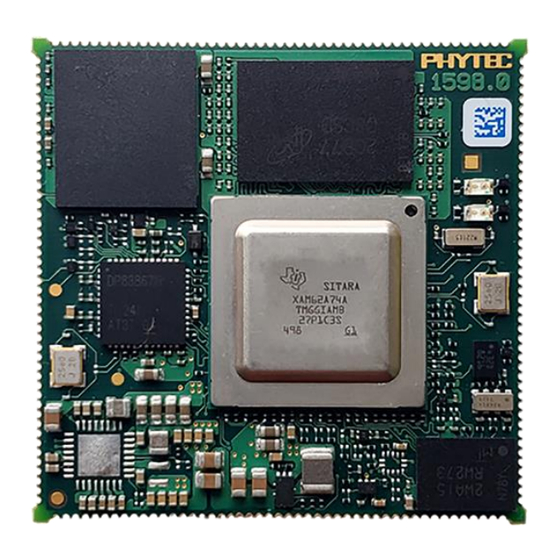
- Page 1 ® phyCORE -AM62Ax Direct Solder Connection (DSC) Hardware Manual Document No.: L-1061e.A0 SOM Prod. No.: PCL-075 SOM PCB. No.: 1598.0 CB Prod. No.: PBA-C-24 CB PCB. No.: 1576.3 Edition: Oct 2023 A product of a PHYTEC Technology Holding company...
-
Page 2: Table Of Contents
PCL-075/phyCORE-AM62Ax DSC System on Module L-1061e.A0 1 Table of Contents Table of Contents ..........................2 List of Figures..........................6 List of Tables ..........................7 SOM Features............................9 Conventions, Abbreviations and Acronyms ................... 10 Conventions ..........................10 Abbreviations and Acronyms ......................10 Types of Signals ........................... - Page 3 PCL-075/phyCORE-AM62Ax DSC System on Module L-1061e.A0 Safe Shutdown and Sudden Power Loss ..................41 System Memory ..........................41 SOM Memory ..........................42 6.1.1 LPDDR4 RAM ........................42 6.1.2 EEPROM ..........................42 6.1.3 eMMC Flash .......................... 42 6.1.4 OSPI ............................. 42 External Memory Bus ........................
- Page 4 PCL-075/phyCORE-AM62Ax DSC System on Module L-1061e.A0 MCASP ............................67 7.7.1 MCASP Pinout ........................67 Display and Camera Interfaces ......................69 VOUT ............................69 8.1.1 VOUT Pinout ......................... 70 CSI .............................. 71 8.2.1 CSI Pinout ..........................71 8.2.2 CSI Design In Considerations....................71 8.2.3...
- Page 5 12.3 WKUP Pinout ..........................90 12.4 RTC ............................. 90 12.4.1 RTC Pinout..........................90 12.5 Heartbeat LEDs ..........................90 13 Integrating and Updating the phyCORE-AM62Ax DSC................91 13.1 Integration ............................ 91 13.2 Modification ..........................91 13.3 In-Field Updates ........................... 91 13.4 Product Change Management....................... 92 14 Additional Information ..........................
-
Page 6: List Of Figures
Figure 3. phyCORE-AM62Ax DSC Dimensions Top View ............... 15 Figure 4. phyCORE-AM62Ax DSC Dimensions End View ............... 16 Figure 5. phyCORE-AM62Ax DSC Component Placement (processor side) .......... 17 Figure 6. phyCORE-AM62Ax DSC Component Placement (connector side) ........... 18 Figure 7. Position Solder Jumper Pad Numbering Scheme ..............20 Figure 8. -
Page 7: List Of Tables
Table 5 Solder Jumper Settings ....................... 20 Table 6 Voltage Domain Configurations ....................21 Table 7 phyCORE-AM62Ax DSC Connector X1, Pins 1-47 Pinout ............28 Table 8 phyCORE-AM62Ax DSC Connector X1, Pins 48-94 Pinout ............29 Table 9 phyCORE-AM62Ax DSC Connector X1, Pins 95-141 Pinout ............30 Table 10 phyCORE-AM62Ax DSC Connector X1, Pins 142-188 Pinout ........... - Page 8 Table 31 VOUT Connections at the SOC footprint ................... 70 Table 32 CSI Connections at the SOC footprint..................71 Table 33 phyCORE-AM62Ax DSC CSI0 Layout Characteristics .............. 72 Table 34 ECAP Connections at the SOC footprint ................... 75 Table 35 EPWM Connections at the SOC footprint .................. 75 Table 36 EQEP Connections at the SOC footprint ...................
-
Page 9: Som Features
PCL-075/phyCORE-AM62Ax DSC System on Module L-1061e.A0 2 SOM Features The phyCORE-AM62Ax Direct Solder Connection (DSC) offers the following features: • Insert-ready, small (40.8 mm x 40.8 mm) System on Module (SOM) subassembly in low EMI design, achieved through advanced SMD technology •... -
Page 10: Conventions, Abbreviations And Acronyms
L-1061e.A0 3 Conventions, Abbreviations and Acronyms This hardware manual describes the PCL-075 System on Module, henceforth referred to as phyCORE-AM62Ax DSC. The manual specifies the phyCORE-AM62Ax DSC's design and function. Precise specifications for the Texas Instruments AM62Ax SoC can be found in the AM62Ax Technical Reference Manual. -
Page 11: Types Of Signals
Peripheral Component Interconnect PCIe PCI express PCM/PCL phyCORE Module (connectorized / direct solder) Product Change Notification PHYTEC Display Interface; defined to connect PHYTEC display adapter boards, or custom adapters PHYTEC Expansion Board PMIC Power management IC Power-on reset Programmable Realtime Unit... - Page 12 PCL-075/phyCORE-AM62Ax DSC System on Module L-1061e.A0 Table 2 Signal Types Used in this Manual Signal Type Description Abbreviation Analog Analog Power Supply voltage input PWR_I Input Digital input Output Digital output Bidirectional input/output OD-Bidir PU Open drain input/output with pull up...
-
Page 13: Introduction
The phyCORE-AM62Ax DSC is a small (40.8 mm x 40.8 mm) insert-ready System on Module populated with the Texas Instrument’s AM62Ax SoC. Its universal design enables its insertion in a wide range of embedded applications. Most of the SoC signals and ports extend from the SoC to the DSC footprint on the bottom of the board, allowing it to be soldered down on a target application. -
Page 14: Block Diagram
PCL-075/phyCORE-AM62Ax DSC System on Module L-1061e.A0 4.1 Block Diagram Figure 2. phyCORE-AM62Ax DSC Block Diagram © PHYTEC America L.L.C. 2023... -
Page 15: Physical Dimensions
PCL-075/phyCORE-AM62Ax DSC System on Module L-1061e.A0 4.2 Physical Dimensions Figure 3. phyCORE-AM62Ax DSC Dimensions Top View © PHYTEC America L.L.C. 2023... - Page 16 PCL-075/phyCORE-AM62Ax DSC System on Module L-1061e.A0 Figure 4. phyCORE-AM62Ax DSC Dimensions End View © PHYTEC America L.L.C. 2023...
-
Page 17: Component Placement Diagram
PCL-075/phyCORE-AM62Ax DSC System on Module L-1061e.A0 4.3 Component Placement Diagram Figure 5. phyCORE-AM62Ax DSC Component Placement (processor side) © PHYTEC America L.L.C. 2023... - Page 18 PCL-075/phyCORE-AM62Ax DSC System on Module L-1061e.A0 Figure 6. phyCORE-AM62Ax DSC Component Placement (connector side) A searchable pdf of the phyCORE-AM62Ax DSC component placement can be found here: here. © PHYTEC America L.L.C. 2023...
-
Page 19: Technical And Electrical Specifications
Connect all ground pins to ground. • Implement a power sequencing circuit to avoid driving external power to the I/O pins of the PHYCORE-AM62Ax DSC SOM before the module is fully powered up. More details on this can be found in section 5.4 Power... -
Page 20: Solder Jumpers
Table 5 provides a functional summary of the solder jumpers which can be changed to adapt the phyCORE-AM62Ax DSC SOM to specific design needs. It shows their default positions, possible alternative positions, type, and functions. The jumpers are a 0201 package size with a 1/16W or higher power rating. - Page 21 Figure 8. Some of the phyCORE-AM62Ax DSC power domains can be configured for 1.8V or 3.3V operation via the solder jumpers in the table above. This allows for configuring the voltage levels of the associated I/O signals under these domains to meet application requirements.
- Page 22 PCL-075/phyCORE-AM62Ax DSC System on Module L-1061e.A0 Figure 8. Jumper Locations (Connector side) © PHYTEC America L.L.C. 2023...
-
Page 23: Pin Descriptions
PCL-075/phyCORE-AM62Ax DSC System on Module L-1061e.A0 4.7 Pin Descriptions Most of the processor signals extend to the DSC footprint on the bottom of the module. Figure 9-11 show recommended landing pattern with dimensions and pin details for soldering down the SOM to a custom carrier board. - Page 24 PCL-075/phyCORE-AM62Ax DSC System on Module L-1061e.A0 Figure 10. Landing Pattern (SOM Edge Dimensions) © PHYTEC America L.L.C. 2023...
- Page 25 PCL-075/phyCORE-AM62Ax DSC System on Module L-1061e.A0 Figure 11. Landing Pattern Detail (SOM Corner Dimensions) © PHYTEC America L.L.C. 2023...
- Page 26 PCL-075/phyCORE-AM62Ax DSC System on Module L-1061e.A0 Figure 12. Landing Pattern Dimensions (Pin Alignment) © PHYTEC America L.L.C. 2023...
- Page 27 Tables 7-10 provide an overview of the pinout of the phyCORE-Connector with signal names and descriptions specific to the phyCORE-AM62Ax SOM as well as the processor ball it connects to, if any. An example of how this information translates to our schematic is shown in Figure 13.
-
Page 28: Pinout Table
PCL-075/phyCORE-AM62Ax DSC System on Module L-1061e.A0 4.8 Pinout Table Table 7 phyCORE-AM62Ax DSC Connector X1, Pins 1-47 Pinout X1, Pins 1-47 SOM Signal Name Type Level Processor Ball Description X_GPMC0_CSn2 3.3V GPMC Chip Select 2 (active low) X_GPMC0_CSn1 3.3V GPMC Chip Select 1 (active low) X_GPMC0_CSn0 3.3V... - Page 29 More information about this signal can be found in section 5 Power This signal should not be driven during reset. More information can be found in section 6.3 System Boot Configuration Table 8 phyCORE-AM62Ax DSC Connector X1, Pins 48-94 Pinout X1, Pins 48-94 Signal Name Type...
- Page 30 The voltage level for this signal is configurable for 1.8V or 3.3V. The default voltage level is listed here, but always check the actual jumper setting for the applicable SOM configuration. Refer to section 4.6 Solder Jumpers for details. Table 9 phyCORE-AM62Ax DSC Connector X1, Pins 95-141 Pinout X1, Pins 95-141 Signal Type...
- Page 31 The voltage level for this signal is configurable for 1.8V or 3.3V. The default voltage level is listed here, but always check the actual jumper setting for the applicable SOM configuration. Refer to section 4.6 Solder Jumpers for details Table 10 phyCORE-AM62Ax DSC Connector X1, Pins 142-188 Pinout X1, Pins 142-188 Processor Signal...
- Page 32 The voltage level for this signal is configurable for 1.8V or 3.3V. The default voltage level is listed here, but always check the actual jumper setting for the applicable SOM configuration. Refer to section 4.6 Solder Jumpers for details. Table 11 phyCORE-AM62Ax DSC Connector X1, Pins 189-270 Pinout X1, Pins 189-270 Processor Signal...
-
Page 33: Thermal Management
75C without an active cooling system (heatsink and fan)). The following parts are used to attach the fan to the phyCORE-AM62Ax DSC SOM processor and to connect the fan power cable to the connector on the PHYTEC phyCORE-AM62Ax DSC Carrier Board:... -
Page 34: Layout Guidelines
PCL-075/phyCORE-AM62Ax DSC System on Module L-1061e.A0 Figure 14. Fan design reference circuit 4.10 Layout Guidelines 4.10.1 High-Speed Differential Signal Routing Guidelines Spacing • Implement proper trace width and spacing to yield the recommended differential impedance value. • Spacing between the differential pairs and other traces should be at least twice the distance between the inter- pair spacing. -
Page 35: General Signal Routing Guidelines
5 Power The following sub-sections discuss the power configuration of the phyCORE-AM62Ax DSC in detail. Table 13 summarizes the relationships between the voltage rails and the devices on the phyCORE-AM62Ax DSC SOM. Table 13 External Supply Voltages Signal Direction Power Draw / Deliver... -
Page 36: Primary System Power (Vin)
VIN supplied to the SOM. For proper operation, the phyCORE-AM62Ax DSC SOM must be supplied with a voltage source of 5V (±5 %) with a minimum 2.5A capacity at the VIN pins on the DSC footprint (if you do not plan to use VDD_3V3_OUT in your custom CB design only 1.25A of capacity is required). - Page 37 PCL-075/phyCORE-AM62Ax DSC System on Module L-1061e.A0 Figure 15. Primary Power VIN(VCC_5V0_MAIN) reference circuit The circuit consists of: • A USB-C connector for connecting an external USB-C power cable to the system • A diode circuit (D49) that will trip in case of an overload preventing damage to the rest of the circuit The reference circuits below showcase additional functionality that can be added to the primary power circuit.
-
Page 38: Backup Power (Vbat)
To keep the Real-Time Clock (RTC) module running, a secondary voltage source of 1.2-5.5V can be supplied to the phyCORE-AM62Ax DSC SOM at the VBAT pin (pin 24 of DSC footprint X1). For the RTC to maintain time when main system power is removed, the VBAT input must be supplied with power. - Page 39 PCL-075/phyCORE-AM62Ax DSC System on Module L-1061e.A0 Most of the reset signals are connected to pullups/pulldowns (X_nRESET_IN also has an attached capacitor) so pullups/pulldowns are not needed on custom CBs for these signals. This information is in Table 14 as well as shown in the figure below.
-
Page 40: Power Sequencing
5.4 Power Sequencing It is mandatory to avoid driving the I/O pins of the phyCORE-AM62Ax DSC SOM when the SOM is not fully powered up. Prematurely driving the pins may cause current to flow through the I/O pins before the processor is properly powered, potentially resulting in damage or unknown behavior after power-up or reset. -
Page 41: Safe Shutdown And Sudden Power Loss
6 System Memory The following sub-sections detail each memory type supported on the phyCORE-AM62Ax DSC as well as how to configure which memory system to boot from. This section is split into memories populated on the SOM and potential CB memory interfaces. -
Page 42: Som Memory
6.1.1 LPDDR4 RAM The RAM on the phyCORE-AM62Ax DSC is comprised of one LPDDR4 SDRAM chip for a 32-bit wide interface providing up to 4GB of SDRAM which can run at up to 4266Mb/s/pin. These chips are connected to the dedicated DDR subsystem of the AM62Ax SOC processor. -
Page 43: External Memory Bus
PCL-075/phyCORE-AM62Ax DSC System on Module L-1061e.A0 Figure 20. OSPI0 CSN signal use 6.2 External Memory Bus 6.2.1 GPMC The General-Purpose Memory Control (GPMC) module can be used as a data path to an external memory device. The GPMC can support: •... - Page 44 PCL-075/phyCORE-AM62Ax DSC System on Module L-1061e.A0 Table 15 GPMC Signal Connections at the SOC footprint Processor Signal X1 Pin #(s) SOM Signal(s) Type Level Description GPMC Address Valid (active low) or Address GPMC0_ADVn_ALE X_GPMC0_ADVn_ALE 3.3V Latch Enable GPMC0_CLK X_GPMC0_CLK 3.3V...
-
Page 45: Sd/Mmc/Sdio
PCL-075/phyCORE-AM62Ax DSC System on Module L-1061e.A0 Processor Signal X1 Pin #(s) SOM Signal(s) Type Level Description X_GPMC0_AD8/BOOTMODE_8 GPMC0_AD8 3.3V GPMC Data 8 Input/Output (100K pullup on SOM) X_GPMC0_AD9/BOOTMODE_9 GPMC0_AD9 3.3V GPMC Data 9 Input/Output (100K pullup on SOM) X_GPMC0_AD10/BOOTMODE_10 GPMC0_AD10 3.3V... - Page 46 SD card power should be connected to a 3.3V power supply regardless of the MMC IO voltage level. • SD card power needs to be toggled with SoC warm reset status (in our reference design we use X_RESETSTATz). Table 17 phyCORE-AM62Ax DSC MMC1 Layout Characteristics © PHYTEC America L.L.C. 2023...
- Page 47 PCL-075/phyCORE-AM62Ax DSC System on Module L-1061e.A0 Signal Name SOM Trace Length (µm) Length Matching (µm) Single Ended Impedance (Ω) X_MMC1_DAT3 26542 X_MMC1_DAT2 25329 X_MMC1_DAT1 25672 12700 X_MMC1_DAT0 25262 X_MMC1_CLK 28221 X_MMC1_CMD 25234 X_MMC2_DAT3 23578 X_MMC2_DAT2 23193 X_MMC2_DAT1 23366 12700 X_MMC2_DAT0...
- Page 48 PCL-075/phyCORE-AM62Ax DSC System on Module L-1061e.A0 Figure 22. MMC1 Load Switch Reference Schematic The circuit consists of: • An SD-card reader with CMD/DATA line pullups • A load switch The second reference circuit connects MMC2 to a E key M.2 connector for use in WIFI/BT applications.
- Page 49 PCL-075/phyCORE-AM62Ax DSC System on Module L-1061e.A0 Figure 24. M.2 WIFI MMC2 Level Translators Reference Schematic The circuit consists of: • A E key M.2 connector to connect to a module • Two voltage translators that serve as buffers for the bootmode signals with jumpers allowing the module to operate at either 3.3V or 1.8V.
-
Page 50: System Boot Configuration
During the power-on reset cycle, the operational system boot mode of the phyCORE-AM62Ax DSC SOM is determined by the configuration of the BOOTMODE [15:0] signals. The BOOTMODE signals must be held at the desired configuration until X_PORz_OUT goes high to be properly latched into the system. - Page 51 To modify the default boot configuration on a custom carrier board, it is recommended to use 1kΩ pull-up resistors or 10kΩ pull-down resistors to override the SOM settings. For startup/verification testing, PHYTEC recommends designing the boot configuration circuit to include a DIP switch. This will make it easy to swap between various boot modes (an example circuit is shown below).
- Page 52 PCL-075/phyCORE-AM62Ax DSC System on Module L-1061e.A0 Figure 26. Reference Schematic for BOOTMODE configuration © PHYTEC America L.L.C. 2023...
-
Page 53: Serial Interfaces
The following sub-sections detail each of the serial interfaces supported on the phyCORE-AM62Ax DSC. 7.1 CAN The phyCORE-AM62Ax DSC SOM provides three Controller Area Network (MCAN) ports. The CAN interfaces support CAN and CAN FD (flexible data-rate) specifications, conforming with CAN protocol version 2.0 part A, B and ISO 11898-1:2015. -
Page 54: Ethernet
PHY if necessary. Refer to the DP83867IRRGZ datasheet for further details on these configuration and strapping options (DP83867IRRGZ Datasheet). NOTE: Adjusting strapping options and PHY registers is not necessary when using PHYTEC provided BSPs. Table 20 Ethernet PHY Default Strapping Configuration Strapping Option Default Setting Strapping Signals... -
Page 55: Ethernet Design In Guide
7.2.2 Ethernet Design In Guide 7.2.2.1 CPSW_ETH0 Ethernet Design In Considerations • Connecting the phyCORE-AM62Ax DSC SOM to an existing 10/100/1000Base-T network involves adding an RJ45 and appropriate magnetic devices in the design. See the reference circuit in section 7.2.3 Ethernet Reference Circuits for an example. - Page 56 PCL-075/phyCORE-AM62Ax DSC System on Module L-1061e.A0 Table 22 phyCORE-AM62Ax DSC CPSW_ETH0 Layout Characteristics Signal Name Length (µm) Intrapair Length Interpair Length Single Ended Differential Matching (µm) Matching (µm) Impedance Impedance Max CB (Ω) (Ω) Trace Total Trace X_CPSW_ETH0_A- 6152 101600...
-
Page 57: Ethernet Reference Circuits
Receive Clock Length Calculation with Physical Trace Delay: (22910 µm) + (Average total length of control/data signals on Carrier Board) + (276860 µm) – (22757 µm) able 24 phyCORE-AM62Ax DSC RGMII2 Trace Length Characteristics Signal Name SOM Trace Length (µm) - Page 58 PCL-075/phyCORE-AM62Ax DSC System on Module L-1061e.A0 Figure 28. RJ45 Reference Schematic The circuit consists of: • An Ethernet Jack • Two TVS diode arrays for ESD protection • Two resistor networks to manage the Ethernet LEDs in the jack Figure 29. RGMII PHY RJ45 Reference Schematic...
- Page 59 PCL-075/phyCORE-AM62Ax DSC System on Module L-1061e.A0 Figure 30. RGMII PHY Strapping Resistors Reference Schematic Figure 31. RGMII PHY Reference Schematic The circuit consists of: • An Ethernet PHY to convert the RGMII signals to differential Ethernet signals © PHYTEC America L.L.C. 2023...
-
Page 60: I 2 C
The Inter-Integrated Circuit (I C) interface is a two-wire, bidirectional serial bus that provides a simple and efficient method for data exchange among devices. The phyCORE-AM62Ax DSC SOM provides six independent multimaster fast-mode I modules. The I C interfaces provide the following functionality: •... -
Page 61: I 2 C Pinout
4.6 Solder Jumpers for details. 7.4 SPI The Serial Peripheral Interface (SPI) is a transmit/receive, master/slave synchronous serial bus. The phyCORE-AM62Ax DSC SOM provides access to four SPI ports at the SOC footprint. 7.4.1 SPI Pinout Table 26 SPI Connections at the SOC footprint... -
Page 62: Uart
CPU. There are ten UART modules provided, and each can be used for configuration and data exchange with external peripheral devices. UART0 is the default console and as such PHYTEC recommends bringing out UART0 for console access. More information on using it as a debug console is provided in section 11.3... - Page 63 PCL-075/phyCORE-AM62Ax DSC System on Module L-1061e.A0 Processor Signal X1 Pin #(s) SOM Signal(s) Type Level Description X_I2C1_SDA UART1_TXD 3.3V UART1 Transmit Data X_MCASP0_ACLKR X_MMC1_DAT0 X_VOUT0_PCLK UART2_CTSN 3.3V UART2 Clear to Send X_GPMC0_AD14/BOOTMODE_14 (100K pulldown on SOM) X_VOUT0_VSYNC X_MMC1_DAT1 UART2_RTSN 3.3V...
- Page 64 PCL-075/phyCORE-AM62Ax DSC System on Module L-1061e.A0 Processor Signal X1 Pin #(s) SOM Signal(s) Type Level Description X_GPMC0_AD14/BOOTMODE_14 (100K pulldown on SOM) X_VOUT0_DATA6 X_VOUT0_DATA7 X_MCAN0_RX UART5_TXD 3.3V UART5 Transmit Data X_MMC2_DAT2 X_GPMC0_AD15/BOOTMODE_15 (100K pulldown on SOM) UART6_CTSN X_VOUT0_DATA11 3.3V UART6 Clear to Send...
-
Page 65: Usb
PCL-075/phyCORE-AM62Ax DSC System on Module L-1061e.A0 7.6 USB The phyCORE-AM62Ax DSC SOM provides two USB2.0 Dual-Role Device (DRD) Subsystems with integrated USB VBUS detection. 7.6.1 USB Pinout Table 28 USB Connections at the SOC footprint X1 Pin #(s) SOM Signal(s) - Page 66 PCL-075/phyCORE-AM62Ax DSC System on Module L-1061e.A0 Figure 32. USB-HUB Reference Schematic Figure 33. USB 2.0 Connector Reference Schematic The above circuits consist of the following parts: • A USB-HUB to convert the USB2.0 and SERDES signals into four USB outputs •...
-
Page 67: Mcasp
Two TVS diode arrays for ESD and EMI considerations • A USB-C connector 7.7 MCASP The phyCORE-AM62Ax DSC SOM provides three Multichannel Audio Serial Ports (MCASP). The MCASP interfaces provide the following functionality: • Supports Time Division Multiplexing (TDM), Inter-IC Sound (I2S), and similar formats •... - Page 68 PCL-075/phyCORE-AM62Ax DSC System on Module L-1061e.A0 MCASP0_AXR1 X_MCASP0_AXR1 3.3V MCASP Serial Data (Input/Output) MCASP0_AXR2 X_MCASP0_AXR2 3.3V MCASP Serial Data (Input/Output) MCASP0_AXR3 X_MCASP0_AXR3 3.3V MCASP Serial Data (Input/Output) X_MMC2_CLK (49.9K pulldown on SOM) MCASP1_ACLKR 3.3V MCASP Receive Bit Clock X_GPMC0_CSn3 X_MMC2_SDCD (10K pullup on...
-
Page 69: Display And Camera Interfaces
8 Display and Camera Interfaces The following sub-sections detail each of the display/camera interfaces supported on the phyCORE-AM62Ax DSC. 8.1 VOUT The phyCORE-AM62Ax DSC SOM brings out one 24-bit RGB parallel video output (VOUT). VOUT supports the following display interface modes: •... -
Page 70: Vout Pinout
PCL-075/phyCORE-AM62Ax DSC System on Module L-1061e.A0 8.1.1 VOUT Pinout Table 31 VOUT Connections at the SOC footprint Processor Signal X1 Pin #(s) SOM Signal(s) Type Level Description VOUT_DE VOUT_DE 3.3V Video Output Data Enable Video Output External Pixel Clock VOUT0_EXTPCLKIN X_GPMC0_WAIT1 3.3V... -
Page 71: Csi
PCL-075/phyCORE-AM62Ax DSC System on Module L-1061e.A0 8.2 CSI The phyCORE-AM62Ax DSC SOM brings out one 4 lane CSI (camera serial interface). The CSI interfaces provide the following functionality: • Compliant with MIPI CSI 1.3 and MIPI-DPHY 1.2 • Support for 1,2,3 or 4 data lane mode up to 2.5Gbps •... -
Page 72: Csi Reference Circuits
8.2.3 CSI Reference Circuits Example reference circuits for connecting the CSI signals to a 30-pin connector are shown below. The 30-pin connector pinout is designed to connect to a PHYTEC camera and supports both 3.3V and 5V cameras. © PHYTEC America L.L.C. 2023... - Page 73 PCL-075/phyCORE-AM62Ax DSC System on Module L-1061e.A0 Figure 35. CSI Power Toggle Reference Schematic © PHYTEC America L.L.C. 2023...
-
Page 74: Control Interfaces
• A 30-pin FFC connector 9 Control Interfaces The following sub-sections detail each of the control interfaces supported on the phyCORE-AM62Ax DSC. 9.1 Enhanced Capture The phyCORE-AM62Ax DSC SOM brings out 3x Enhanced Capture (ECAP) modules. © PHYTEC America L.L.C. 2023... -
Page 75: Ecap Pinout
SOM configuration. Refer to section 4.6 Solder Jumpers for details. 9.2 Enhanced Pulse-Width Modulation The phyCORE-AM62Ax DSC SOM supports up to four Enhanced Pulse-Width Modulation (PWM) modules. Each PWM provides the following functionality: • A dedicated 16-bit time-base counter with period and frequency control. -
Page 76: Enhanced Quadrature Encoder Pulse
The voltage level for this signal is configurable for 1.8V or 3.3V. The default voltage level is listed here, but always check the actual jumper setting for the applicable SOM configuration. Refer to section 4.6 Solder Jumpers for details. 10 Peripheral Interfaces The following sub-sections detail each of the peripheral interfaces supported on the phyCORE-AM62Ax DSC. © PHYTEC America L.L.C. 2023... -
Page 77: Cpts
PCL-075/phyCORE-AM62Ax DSC System on Module L-1061e.A0 10.1 CPTS The phyCORE-AM62Ax DSC SOM brings out the Common Platform Time Sync (CPTS) module that is used to facilitate host control of time sync operations. 10.1.1 CPTS Pinout Table 37 CPTS Connections at the SOC footprint... -
Page 78: Gpio Pinout
PCL-075/phyCORE-AM62Ax DSC System on Module L-1061e.A0 Many of the GPIOs are multiplexed with other interfaces, some of which connect to on-board circuits. Review the tables below when using these GPIOs to check for pull-up and pull-down resistors, connected devices, etc. - Page 79 PCL-075/phyCORE-AM62Ax DSC System on Module L-1061e.A0 Processor X1 Pin #(s) SOM Signal(s) Type Level Internal SOM Usage Signal GPIO0_37 X_GPMC0_WAIT0 3.3V None GPIO0_38 X_GPMC0_WAIT1 3.3V None GPIO0_39 X_GPMC0_WPn 3.3V None GPIO0_40 X_GPMC0_DIR 3.3V None GPIO0_41 X_GPMC0_CSn0 3.3V None GPIO0_42 X_GPMC0_CSn1 3.3V...
- Page 80 PCL-075/phyCORE-AM62Ax DSC System on Module L-1061e.A0 Table 40 GPIO1 Accessibility at SOC footprint Processor X1 Pin #(s) SOM Signal(s) Type Level Internal SOM Usage Signal GPIO1_0 X_CPSW_RGMII2_TD3 3.3V None GPIO1_1 X_CPSW_RGMII2_RX_CTL 3.3V None GPIO1_2 X_CPSW_RGMII2_RXC 3.3V None GPIO1_3 X_CPSW_RGMII2_RD0 3.3V...
-
Page 81: Timer
4.6 Solder Jumpers for details. 10.3 TIMER The phyCORE-AM62Ax DSC SOM brings out 12x Timer modules. The modules have a 32-bit data bus width and provide interrupts generated on overflow, compare, and capture. 10.3.1 Timer Pinout Table 42 Timer Signals... -
Page 82: Debug Interfaces
The following sub-sections detail each of the debug interfaces supported on the phyCORE-AM62Ax DSC. 11.1 JTAG The phyCORE-AM62Ax DSC SOM is equipped with a JTAG interface for downloading program code into the internal RAM or for debugging programs currently executing. The JTAG interface is accessible via the SOC footprint and provides seven standard IEEE1149.6 JTAG signals. -
Page 83: Jtag Reference Circuit
PCL-075/phyCORE-AM62Ax DSC System on Module L-1061e.A0 11.1.2 JTAG Reference Circuit An example reference circuit for connecting the JTAG signals to a 2x20 connector is shown below. Note that the pinout is based on TI’s compact 20-pin JTAG connector setup. More details on the specifics of that pinout can be found here... -
Page 84: Trace (Trc)
PCL-075/phyCORE-AM62Ax DSC System on Module L-1061e.A0 11.2 TRACE (TRC) The phyCORE-AM62Ax DSC SOM is equipped with a TRACE (TRC) module that can be used to record operation of the ROM code and debug unexpected occurrences. 11.2.1 TRC Pinout Table 44 TRC Connections at the SOC footprint... -
Page 85: Uart0
6.3 System Boot Configuration. 11.3 UART0 The phyCORE-AM62Ax DSC SOM can also be communicated with using UART0 for downloading program code into the internal RAM or for debugging programs currently executing. UART0 is the default console and as such PHYTEC recommends bringing out UART0 for console access. - Page 86 PCL-075/phyCORE-AM62Ax DSC System on Module L-1061e.A0 Figure 38. UART0 to USB Bridge Reference Schematic © PHYTEC America L.L.C. 2023...
- Page 87 PCL-075/phyCORE-AM62Ax DSC System on Module L-1061e.A0 Figure 39. UART0 to USB Buffers and Regulator Reference Schematic The circuit consists of: • Four buffers to isolate the UART signals from the bridge/header until SOM power is brought up and PGOOD has gone high (this is important as driving these signals high to early will prevent the SOM from powering on) •...
- Page 88 PCL-075/phyCORE-AM62Ax DSC System on Module L-1061e.A0 • A TVS diode array for ESD protection • A micro-USB connector • A DC regulator to convert the 5V USB power to 3.3V A simpler design that just brings out the bare minimum UART signals for use with FTDI USB adapter cables is shown below.
-
Page 89: System Interfaces
PCL-075/phyCORE-AM62Ax DSC System on Module L-1061e.A0 12 System Interfaces The following sub-sections detail the system signals brought out to the phyCORE connectors from the MAIN, MCU, and WKUP domains of the AM62Ax processor that are not discussed elsewhere in the manual. It also covers the on-board RTC and the two heartbeat LEDs. -
Page 90: Wkup Pinout
12.5 Heartbeat LEDs The phyCORE-AM62Ax has two LEDs, one green (connected to the Linux domain) and one red (connected to the MCU domain), named the heartbeat LEDs. In PHYTEC’s software, the green LED is configured to flash in a heartbeat pattern once the SOM starts booting into Linux. -
Page 91: Integrating And Updating The Phycore-Am62Ax Dsc
The various reference circuits contained in sections 5-12 as well as the information in section Minimum Requirements for Operation can be used as a starting point for integrating the phyCORE-AM62Ax DSC SOM into target circuitry. Additional information is available to facilitate the integration of the phyCORE-AM62Ax DSC SOM into customer applications, such as: phyCORE-AM62Ax SOM and Carrier Board Schematic References: •... -
Page 92: Product Change Management
13.4 Product Change Management Use of PHYTEC products ensures interchangeable SoC core circuitry in the event of obsolescence of parts used on our SOMs and SBCs. End users no longer need to redesign entire CPU circuitry and engage in version control to accommodate new or obsolete parts. -
Page 93: Additional Information
PHYTEC System on Modules (SOM) and Single Board Computers (SBC) are designed as subcomponents for integration in electrical devices. Combined with PHYTEC Carrier Boards, PHYTEC SOMs can be used as dedicated Evaluation Boards (i.e.: for use as a test and prototype platform for hardware/software development) in laboratory environments. - Page 94 - are reserved. No reproduction may occur without the express written consent from PHYTEC. The information in this document has been carefully checked and is as reliable as possible. However, PHYTEC assumes no responsibility for any inaccuracies. PHYTEC neither gives any guarantee nor accepts any liability whatsoever for consequential damages resulting from the use of this manual or its associated product.
-
Page 95: Revision History
PCL-075/phyCORE-AM62Ax DSC System on Module L-1061e.A0 15 Revision History Table 50 Document Revision History Date Version Number Changes in this Manual 2023/10/30 L-1061e.A0 Preliminary Release © PHYTEC America L.L.C. 2023...
Need help?
Do you have a question about the phyCORE-AM62Ax and is the answer not in the manual?
Questions and answers