ST STM32 Nucleo User Manual
Hide thumbs
Also See for STM32 Nucleo:
- User manual (85 pages) ,
- Application note (49 pages) ,
- Quick start manual (31 pages)
Table of Contents
Advertisement
Quick Links
UM2953
User manual
STM32 Nucleo-64 board (MB1717)
Introduction
The STM32 Nucleo-64 board, based on the MB1717 reference board
(NUCLEO-C031C6
order code) provides an affordable
and flexible way for users to try out new concepts and build prototypes with various combinations of performance, power
consumption, and features.
®
The ARDUINO
Uno V3 connectivity support and the ST morpho headers provide an easy means of expanding the functionality
of the STM32C0 Nucleo open development platform with a wide choice of specialized shields.
The STM32 Nucleo-64 board does not require any separate probe, as it integrates the ST-LINK/V2-1 debugger/programmer.
The STM32 Nucleo-64 board comes with the comprehensive free STM32 software libraries and examples that are available with
the
STM32CubeC0
MCU Package.
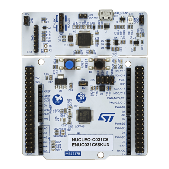
Figure 1.
NUCLEO-C031C6 board (Top view)
Picture is not contractual.
UM2953 - Rev 1 - February 2022
www.st.com
For further information contact your local STMicroelectronics sales office.
Advertisement
Table of Contents

Related Manuals for ST STM32 Nucleo


Summary of Contents for ST STM32 Nucleo
-
Page 1: Figure 1. Nucleo-C031C6 Board (Top View)
STM32C0 Nucleo open development platform with a wide choice of specialized shields. The STM32 Nucleo-64 board does not require any separate probe, as it integrates the ST-LINK/V2-1 debugger/programmer. The STM32 Nucleo-64 board comes with the comprehensive free STM32 software libraries and examples that are available with STM32CubeC0 MCU Package. -
Page 2: Features
® – ARDUINO Uno V3 expansion connector – ST morpho extension pin headers for full access to all STM32C0 I/Os • Flexible power-supply options: ST-LINK USB V or external sources • On-board ST-LINK/V2-1 debugger/programmer with USB re-enumeration capability: mass storage, Virtual COM port, and debug port •... -
Page 3: Ordering Information
UM2953 Ordering information Ordering information To order the NUCLEO-C031C6 Nucleo-64 board, refer to Table 1. Additional information is available from the datasheet and reference manual of the target STM32. Table 1. Ordering information Order code Board reference Target STM32 NUCLEO-C031C6 MB1717 STM32C031C6T6 Codification... -
Page 4: Development Environment
STM32 flash memory for easy demonstration of the device peripherals in standalone mode. The latest versions of the demonstration source code and associated documentation can be downloaded from www.st.com. UM2953 - Rev 1 page 4/32... -
Page 5: Conventions
UM2953 Conventions Conventions Table 3 provides the conventions used for the ON and OFF settings in the present document. Table 3. ON/OFF convention Convention Definition Jumper JPx ON Jumper fitted Jumper JPx OFF Jumper not fitted Jumper JPx [1-2] Jumper fitted between Pin 1 and Pin 2 Solder bridge SBx ON SBx connections closed by 0 Ω... -
Page 6: Quick Start
® To power the board, connect the STM32 Nucleo-64 board to a PC with a USB Type-A or USB Type-C Micro-B cable through the CN1 USB connector. Once powered on, the LD3 PWR green LED lights up and LD1 COM LED blinks. -
Page 7: Hardware Layout And Configuration
Uno V3 connector, ST morpho connector, push‑button, and embedded ST-LINK/V2-1). Figure 3 Figure 4 help the user to locate these features on the STM32 Nucleo-64 board. The mechanical dimensions of the NUCLEO-C031C6 product are shown in Figure Figure 2. Hardware block diagram... -
Page 8: Figure 3. Nucleo-C031C6 Pcb Top Side
UM2953 Hardware layout and configuration Figure 3. NUCLEO-C031C6 PCB top side UM2953 - Rev 1 page 8/32... -
Page 9: Figure 4. Nucleo-C031C6 Pcb Bottom Side
UM2953 Hardware layout and configuration Figure 4. NUCLEO-C031C6 PCB bottom side UM2953 - Rev 1 page 9/32... -
Page 10: Stm32 Nucleo-64 Board Mechanical Drawing
UM2953 STM32 Nucleo-64 board mechanical drawing STM32 Nucleo-64 board mechanical drawing Figure 5. STM32 Nucleo-64 board mechanical dimensions (in millimeters) UM2953 - Rev 1 page 10/32... -
Page 11: Default Board Configuration
Cuttable PCB The STM32 Nucleo-64 board is divided into two parts: the ST-LINK part and the target MCU part. The ST-LINK PCB part is cuttable to reduce the board size. In this case, the remaining target MCU part is only powered by VIN, ®... -
Page 12: St-Link/V2-1 Firmware Upgrade
UM2953 Embedded ST-LINK/V2-1 In cases where the STM32 Nucleo-64 board is connected to the PC before the driver is installed, some STM32 Nucleo-64 interfaces might be declared as “Unknown” in the PC device manager. In this case, the user must... -
Page 13: Power Supply And Power Selection
5V_ST_LINK is a DC power with limitations from the ST-LINK USB connector (USB type Micro-B connector of ST-LINK/V2-1). In this case, the JP5 jumper must be on pins 1 and 2 to select the STLK power source on the JP5 silkscreen. -
Page 14: External Power Supply Output
VIN is the 7 to 12 V DC power from CN6 pin 8 named VIN on ARDUINO connector silkscreen or from pin 24 of CN7 ST morpho connector. In this case, the JP5 jumper must be [3-4] to select the VIN power source on the ®... -
Page 15: Lse Clock Reference
R33 and R34 OFF MCO from ST-LINK: MCO output of ST-LINK is used as an input clock. This frequency cannot be changed, it is fixed at 8 MHz and connected to the PF0-OSC_IN of the STM32 microcontroller. The configuration must –... -
Page 16: Vcp Communication
LEDs Four LEDs are available on the STM32 Nucleo-64 board. The four LEDs are located on the top side of the board: LD1 COM: LD1 is a bi-colored LED. the LD1 default status is red. LD1 turns to green to indicate that communication is in progress between the PC and the ST-LINK/V2-1 as follow: –... -
Page 17: Jumper Configuration
SWD interface SB11/SB13/SB15/SB17 Reserved, do not modify. (Default) SWD interface SB12/SB14/SB16/SB18 Reserved, do not modify. (Reserved) VCP interface VCP connects ST-LINK and on‑board MCU. (Default) SB21/SB22 VCP interface VCP interface used as GPIOs (Reserved) 100 mA maximum allowed current through CN1... - Page 18 UM2953 Solder bridge configuration Solder bridge Definition State Comment U6 LDO output provides 3.3 V. 3.3 V LDO output U6 LDO output does not provide 3.3 V. SB27/SB32 ON, USART2 from PA2/PA3 SB31/SB33 OFF SB27/SB31/ UART for VCP SB32/SB33 SB27/SB32 OFF, USART1 from PB6/PB7 SB31/SB33 ON VDD provides power to...
-
Page 19: Connectors
UM2953 Connectors Connectors Seven connectors are implemented on the STM32 Nucleo-64 board: • CN1 ST-LINK USB Micro-B connector ® • CN5, CN6, CN8, and CN9 ARDUINO Uno V3 connector • CN7 and CN10 ST morpho connectors ® ARDUINO Uno V3 connector ®... -
Page 20: Cn7 And Cn10 St Morpho Connectors
ARD_D0 UART_1_RX CN7 and CN10 ST morpho connectors The CN7 and CN10 ST morpho connectors are male pin headers accessible on both sides of the STM32 Nucleo-64 board (Refer to Figure 3). All STM32 signals and power pins except 1.2 V VDD_CORE are available on the ST morpho connectors. -
Page 21: Stm32 Nucleo-64 Board Information
Evaluation tools marked as “ES” or “E” are not yet qualified and therefore not ready to be used as reference design or in production. Any consequences deriving from such usage will not be at ST charge. In no event, ST will be liable for any customer usage of these engineering sample tools as reference designs or in production. -
Page 22: Nucleo-C031C6 Stm32 Nucleo-64 Board I/O Assignment
UM2953 NUCLEO-C031C6 STM32 Nucleo-64 board I/O assignment NUCLEO-C031C6 STM32 Nucleo-64 board I/O assignment Table 12. NUCLEO-C031C6 STM32 Nucleo-64 board I/O assignment Pin number Pin name Main feature / optional feature PC13 BUTTON PC14-OSC32_IN OSC32_IN PC15-OSC32_OUT OSC32_OUT VREF+ PF0-OSC_IN OSC_IN PF1-OSC_OUT... - Page 23 UM2953 NUCLEO-C031C6 STM32 Nucleo-64 board I/O assignment Pin number Pin name Main feature / optional feature ARD_D3 || TIM1_CH2 ARD_D5 || TIM3_CH1 ARD_D6 || TIM3_CH3 ARD_D1 || VCP_USART1_TX ARD_D0 || VCP_USART1_RX ARD_D14_I2C_SDA ARD_D15_I2C_SCL UM2953 - Rev 1 page 23/32...
-
Page 24: Federal Communications Commission (Fcc) And Innovation, Science And Economic
UM2953 Federal Communications Commission (FCC) and Innovation, Science and Economic Development Canada (ISED) Compliance Statements Federal Communications Commission (FCC) and Innovation, Science and Economic Development Canada (ISED) Compliance Statements 10.1 FCC Compliance Statement Part 15.19 This device complies with Part 15 of the FCC Rules. Operation is subject to the following two conditions: (1) this device may not cause harmful interference, and (2) this device must accept any interference received, including interference that may cause undesired operation. - Page 25 UM2953 IC Compliance Statement Déclaration de conformité Avis: Le présent appareil est conforme aux CNR d'Industrie Canada applicables aux appareils radio exempts de licence. L'exploitation est autorisée aux deux conditions suivantes : (1) l'appareil ne doit pas produire de brouillage, et (2) l'utilisateur de l'appareil doit accepter tout brouillage radioélectrique subi, même si le brouillage est susceptible d'en compromettre le fonctionnement.
-
Page 26: Ce Conformity
UM2953 CE conformity CE conformity 11.1 Warning EN 55032 / CISPR32 (2012) Class B product Warning: this device is compliant with Class B of EN55032 / CISPR32. In a residential environment, this equipment may cause radio interference. Avertissement : cet équipement est conforme à la Classe B de la EN55032 / CISPR 32. Dans un environnement résidentiel, cet équipement peut créer des interférences radio. -
Page 27: Revision History
UM2953 Revision history Table 13. Document revision history Date Version Changes 16-Feb-2022 Initial release. UM2953 - Rev 1 page 27/32... -
Page 28: Table Of Contents
STM32 Nucleo-64 board mechanical drawing........ - Page 29 Board MB1717 revision B01 ..........21 NUCLEO-C031C6 STM32 Nucleo-64 board I/O assignment ......22 Federal Communications Commission (FCC) and Innovation, Science and Economic Development Canada (ISED) Compliance Statements .
-
Page 30: List Of Tables
NUCLEO-C031C6 STM32 Nucleo-64 board I/O assignment ........ -
Page 31: List Of Figures
STM32 Nucleo-64 board mechanical dimensions (in millimeters)....... . . 10... - Page 32 ST’s terms and conditions of sale in place at the time of order acknowledgement. Purchasers are solely responsible for the choice, selection, and use of ST products and ST assumes no liability for application assistance or the design of Purchasers’...
Need help?
Do you have a question about the STM32 Nucleo and is the answer not in the manual?
Questions and answers