Table of Contents
Advertisement
Quick Links
Description
The ZSSC324x SSC Evaluation Kit is designed for sensor module
evaluation, laboratory setup, and module calibration development
for the ZSSC324x Sensor Signal Conditioner (SSC).
The main purpose of the ZSSC324x Evaluation Kit is to enable the
communication between the user and the ZSSC324x device with
the GUI (Graphical User Interface). The ZSSC324x-GUI
establishes the communication via a USB port (configured as a
virtual COM port) to the SSC Communication Board (CB). The
microcontroller on the SSC CB interprets these commands,
converts them to the configured interface (I2C, SPI or OWI), and
provides it to the ZSSC324x located on the ZSSC324x SSC
Evaluation Board.
Almost all possible applications can be tested with the Evaluation
Kit and the GUI, so that the customer can easily get the first
experience and also evaluate in detail the ZSC324x functionalities.
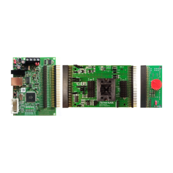
Kit Contents
ZSSC324x Evaluation Board -ZSSC324xEVB
SSC Communication Board
SRB (Sensor Replacement Board)
SSCSENSORREPBDV2P0
ZSSC324x 24-PQFN 4 × 4 mm Samples (5 pcs)
USB Cable
ZSSC324x Demo Kit
© 2020 Renesas Electronics Corporation
ZSSC324x Evaluation Kit User Manual
- SSCCOMMBOARDV4P1C
Features
I2C, SPI or OWI communication interface enables quick and
easy configuration and calibration of the ZSSC324x using the
user's computer.
Connections are provided on the ZSSC324x SSC Evaluation
Board for user's sensor module, which can be used instead
of the SSC Sensor Replacement Board.
A potentiometer on the SSC Sensor Replacement Board
controls a voltage that simulates a sensor signal ranging
from 2mV to 110mV, which can be input to the analog
frontend of the ZSSC324x (INP and INN pins) for evaluation
of basic features or for demonstrating a "dry-run" calibration.
Modular design allows reuse of kit components for evaluation
of select ZSSC324x products.
Clamshell 24-PQFN socket for ZSSC324x device under test
(DUT) facilitates testing multiple DUTs without soldering.
Software is available for download from the Renesas web site.
Note: The SSC Communication Board must have the V4.12
firmware (or higher version) in order to recognize the ZSSC324x. If
using an older Communication Board, contact Renesas regarding
firmware update procedures. For more detailed information about
the SSC Communication Board, refer to the SSC Communication
Board Data Sheet available at www.IDT.com/SSC-COMM-BD.
1
April 15, 2020
Advertisement
Table of Contents

Related Manuals for Renesas ZSSC3240KIT


Summary of Contents for Renesas ZSSC3240KIT
- Page 1 Clamshell 24-PQFN socket for ZSSC324x device under test experience and also evaluate in detail the ZSC324x functionalities. (DUT) facilitates testing multiple DUTs without soldering. Software is available for download from the Renesas web site. Kit Contents Note: The SSC Communication Board must have the V4.12 firmware (or higher version) in order to recognize the ZSSC324x.
-
Page 2: Table Of Contents
ZSSC324x Kit User Manual Important Notes Disclaimer Integrated Device Technology, Inc. and its affiliated companies (herein referred to as “Renesas”) shall not be liable for any damages arising out of defects resulting from delivered hardware or software (ii) non-observance of instructions contained in this manual and in any other documentation provided to user, or (iii) misuse, abuse, use under abnormal conditions, or alteration by anyone other than Renesas. - Page 3 Figure 5. Jumpers on the SSC Communication Board and the ZSSC324x EVB ..................13 Figure 6. Lab Equipment Connections ..............................14 Figure 7. LEDs Status CB - Ready for Operation (without GUI Running) ....................15 © 2020 Renesas Electronics Corporation April 15, 2020...
- Page 4 Figure 47. Saturation Condition ................................... 41 Figure 48. Calibration Points Set Options ..............................41 Figure 49. 2-Points Calibration – Reference Points ............................. 41 Figure 50. 2-Points Calibration – Points Position ............................42 © 2020 Renesas Electronics Corporation April 15, 2020...
- Page 5 Table 10. IC Status Indicators ..................................26 Table 11. Supported Default Calibration Types ............................32 Table 12. Jumper Settings for Amplified Analog Output ..........................48 Table 13. Abbreviations and terms used in the document.......................... 51 © 2020 Renesas Electronics Corporation April 15, 2020...
-
Page 6: Evaluation Kit Setup
The ZSSC324x power (VDD) can be supplied by the user’s external power supply. See 1.7 for connection details. • DC Voltmeter 0-50V and DC Ampmeter (0-100mA) • 4 channel 100MHz Oscilloscope • © 2020 Renesas Electronics Corporation April 15, 2020... -
Page 7: User Computer Requirements And Setup
The ZSSC324x Evaluation Software required for the kit is not included with the kit. To ensure use of the latest version of the software, it is available for download in zip file format from the Renesas web site. Note: FTDI USB drivers are needed for communication. If these drivers are not already installed on the user’s computer, they can be downloaded from the FTDIs homepage, https://www.ftdichip.com/FTDrivers.htm. -
Page 8: Figure 2. Zssc324X Ssc Evaluation Board - Overview
ZSSC324x Kit User Manual Figure 2. ZSSC324x SSC Evaluation Board – Overview Table 1. Sensor Signal at Connectors Signal VDDB VSSB © 2020 Renesas Electronics Corporation April 15, 2020... -
Page 9: Figure 3. Signal Connections: Ssc Communication Board And Zssc324X Evb
Signals are highlighted on Figure 3 Figure 3. Signal Connections: SSC Communication Board and ZSSC324x EVB For a complete description of the SSC CB, refer to the relevant datasheet available at the following link: https://www.idt.com/products/sensor-products/sensor-signal-conditioners/ssc-cb-ssc-communication-board. © 2020 Renesas Electronics Corporation April 15, 2020... -
Page 10: Figure 4. Signal Connections: Zssc324X Evb And Srb
VDDB Bridge positive supply voltage Bridge positive signal Bridge negative signal Refer to Figure 4, to display the odd numbered pins on the PCB. Figure 4. Signal Connections: ZSSC324x EVB and SRB © 2020 Renesas Electronics Corporation April 15, 2020... -
Page 11: Table 5. Evaluation Board Connections Descriptions
KS5V rail, from the CB. Short pins 1-2. • KS12V rail, from the CB. Short pins 2-3. • For current loop operation a jumper connecting pins 2-3 must be inserted. • 2-Pin Header – Male HW identification © 2020 Renesas Electronics Corporation April 15, 2020... -
Page 12: Kit Hardware Connections (Default)
Figure 5. An ESD safe vacuum suction pen should be used for correct handling of the ICs. The smallest suction cup is best suited for the ZSSC324x samples. The assembled kit looks like as per Figure 1, with jumpers as per Figure 5. See section 1.6 for the steps regarding the external lab equipment connections. © 2020 Renesas Electronics Corporation April 15, 2020... -
Page 13: Communication Interfaces
The ZSSC324x Evaluation Board is using the SSC CB to translate these interfaces to USB. Only one SSC CB can be connected to the user’s computer to operate GUI normally. The ZSSC324x Evaluation Software is intended for demonstration purposes and calibration of single units. Upon request, Renesas provides the user with algorithms and assistance in developing their full production calibration software. -
Page 14: Power Supply Option
Important: The maximum voltage for an external supply is 48V. If using an external power supply, do not apply the power connection until jumpers are properly set and HV option has been selected in the GUI. © 2020 Renesas Electronics Corporation April 15, 2020... -
Page 15: Power-Up Procedure
ZSSC324x is powered from the KS5V rail of the SSC CB. Additionally, the IC status section of the GUI reflects this by highlighting the virtual LEDs Powered and CMD Mode Figure 9. The kit is now ready to use. © 2020 Renesas Electronics Corporation April 15, 2020... -
Page 16: Figure 8. Led Status After Starting The Evaluation Sw
ZSSC324x Kit User Manual Figure 8. LED Status after Starting the Evaluation SW Figure 9. Initial GUI Display © 2020 Renesas Electronics Corporation April 15, 2020... -
Page 17: Gui
This section controls the file operations regarding the NVM content and the communication interface setup of the ZSSCC324x device. 2.1.1 NVM Control The content of the NVM can be Saved or Loaded from the File menu. © 2020 Renesas Electronics Corporation April 15, 2020... -
Page 18: Interface Setup
Information on how to write the data to ZSSC324x device is presented in section 2.7.2. Before loading the NVM, stop any ongoing measurements. 2.1.2 Interface Setup This menu allows setup of the communication interfaces: OWI, SPI and I2C. © 2020 Renesas Electronics Corporation April 15, 2020... -
Page 19: Figure 12. Communication Interface Setup Spi
. If the default address is changed, the Slave-address needs to be changed on this sub-tab. Figure 14. Communication Interface Setup - OWI For using the above serial interfaces, the correct jumper setting is required before attempting to establish communication, see Table 7. © 2020 Renesas Electronics Corporation April 15, 2020... -
Page 20: Output Interrupt Signaling
Information Bar: Status window message for a successful I2C scan: Valid I2C address found: 0xXX! Status window message for an I2C scan without slave acknowledge: No valid I2C address found! © 2020 Renesas Electronics Corporation April 15, 2020... -
Page 21: Measurement Control
The first stops the Cyclic Mode, the second sets the IC in Command Mode (CM). Note: In Cyclic Mode, the ZSSC324x always provides BUSY=1 (see Figure 17) until the STOP_CYC (Command BF ) command is sent. © 2020 Renesas Electronics Corporation April 15, 2020... -
Page 22: Figure 17. Cyclic Measurements - Busy Status
, not cyclic) are performed and the resulting mean value is provided as output Oversample-16 Measure - mean value generation; 16 full measurements (like triggered with AA , not cyclic) are performed and the resulting mean value is provided as output © 2020 Renesas Electronics Corporation April 15, 2020... -
Page 23: Display Control
The original stream of bits can be viewed by logging the communication. The graph shown in Figure 19 is an example of the resolution range from the chip through the communication channel to the GUI display. © 2020 Renesas Electronics Corporation April 15, 2020... -
Page 24: Logging Options
In Figure 21, Figure 22, and Figure 23, examples of command logs in case of SPI, I2C and OWI serial interfaces communication are shown. Figure 21. Communication log SPI Figure 22. Communication log I2C © 2020 Renesas Electronics Corporation April 15, 2020... -
Page 25: Measurement Data Log
The status is updated automatically for any reading sequence from the ZSSC324x. It can also be updated manually by clicking on the Status Request button. Table 10 shows the meaning of the various status indicators according to relevant background color. Figure 24. IC status © 2020 Renesas Electronics Corporation April 15, 2020... -
Page 26: Hardware Connection
The ZSSC324x is in Sleep Mode. Test Mode The ZSSC324x is Not in Test Mode. Test Mode Test Mode The ZSSC324x is in Test Mode (only for Renesas use). Cyclic Mode The ZSSC324x is not in Cyclic Mode. Cyclic Mode Cyclic Mode The ZSSC324x is in Cyclic Mode. -
Page 27: Sensor And Temperature Readings
The user can change the register content in the NVM table by modifying the desired value directly in the table, or by using the drop down menus of the single parameters. For more information regarding the drop down menu settings, refer to the ZSSC324x datasheet. © 2020 Renesas Electronics Corporation April 15, 2020... -
Page 28: Figure 27. Nvm Table
ZSSC324x must be in Command Mode or Sleep Mode in order to write to the NVM. Figure 27. NVM Table address Modified register Selected register Modified register, that failed to be written in the last attempt © 2020 Renesas Electronics Corporation April 15, 2020... -
Page 29: Figure 28. Sm Config 1/2 Sub-Tab
The controls provided are changing the content of registers 03 and are shown in Figure 30. For a description of the registers down to bit level, refer to the ZSSSC3240 Data Sheet © 2020 Renesas Electronics Corporation April 15, 2020... -
Page 30: Calibration Tab
The tab is divided into three main areas: Calibration points positions – provides visual representation of the calibration points. Calibration points – allows selection of the calibration type. Coefficients – shows the calculated calibration coefficients. © 2020 Renesas Electronics Corporation April 15, 2020... -
Page 31: Figure 32. Calibration Tab
Above the Calibration Points Position area (see Figure 32), the calibration type can be selected in a drop-down menu. Available default calibration types are described in Table 11. © 2020 Renesas Electronics Corporation April 15, 2020... -
Page 32: Diagnostic / Cyclic Configuration / Command Section
2.7.4 Diagnostic / Cyclic Configuration / Command Section In Figure 34 the overview of the tab is provided. There are 5 sub-tab areas that are discussed in sections 2.7.4.1, 2.7.4.2, 2.7.4.3, 2.7.4.4, and 2.7.4.5. © 2020 Renesas Electronics Corporation April 15, 2020... -
Page 33: Figure 34. Diagnostic / Cyclic Configuration /Command Section
ZSSC324x Data Sheet for a detailed description of the continuously running measurement sequence. In Figure 35, the registers affected by each parameter in this sub-tab are shown. Refer to the register map in the datasheet for a detailed description of the function of each bit. Figure 35. Cyclic Operation Parameters © 2020 Renesas Electronics Corporation April 15, 2020... -
Page 34: Figure 36. Adc And Dac Diagnostics
. Those commands are described in the ZSSC324x Data Sheet. For a new status check, click the Reset Diagnostic button and then, to verify the status of the diagnostic, click the Apply Sensor Check button. © 2020 Renesas Electronics Corporation April 15, 2020... -
Page 35: Figure 37. Sensor Check Selection Settings
These commands are not part of the ZSSC324x command set. The controller on the CB interprets them and switches on /off the 12V for HV application on the EVB. LED L3 is indicating whether this voltage is available on the EVB (see Figure 2 and Table 2) © 2020 Renesas Electronics Corporation April 15, 2020... -
Page 36: Main Buttons
Start/Stop – Trigger the start and stop of measurements acquisition. Its label toggles according to the relevant status. Get Measurements Value for Calibration – It Is used in combination with the Calibration tab (see section 2.7.3). © 2020 Renesas Electronics Corporation April 15, 2020... -
Page 37: Information Bar
This bar returns a status message when specific status is requested. An example is shown in Figure 41, where, using the I2C interface, and a scan of the addresses of the bus is requested by clicking on the Scan I2C-Bus button. Figure 41. Information Bar Message © 2020 Renesas Electronics Corporation April 15, 2020... -
Page 38: Calibration Process, Configuration And Calibration Example
(SRB) to emulate a sensor signal. A typical calibration flow includes the five basic steps: 1. Setup and initialization, see section 3.3. 2. Data collection, see section 3.4. 3. Coefficient calculation, see section 3.5. © 2020 Renesas Electronics Corporation April 15, 2020... -
Page 39: Connect Evk And Start Gui
In this example it is used a gain of 30, but it can vary due to the resistor tolerances of the SRB. Settings are summarized in Figure 44. © 2020 Renesas Electronics Corporation April 15, 2020... -
Page 40: Figure 44. Afe Settings
The same configuration of the AFE could also cause a saturation at the top (or bottom) limit of the full scale output, as it is illustrated in the Figure 47. In this case, it is recommended to reduce the gain or increase offset value. © 2020 Renesas Electronics Corporation April 15, 2020... -
Page 41: Data Collection
The graph for Calibration Points Position provides the view as shown in Figure 50, where the x-axes represents the temperature and the y-axes the percentage of the full scale for the bridge sensor. © 2020 Renesas Electronics Corporation April 15, 2020... -
Page 42: Figure 50. 2-Points Calibration - Points Position
External Sensor numerical display shows 90%. Stop the measurement, and click the Get Measurement Value for Calibration button in the bottom left corner of the GUI. The table on the Calibration Points sub-tab is filled with relevant raw values in the S[count] column, as displayed in Figure 52. © 2020 Renesas Electronics Corporation April 15, 2020... -
Page 43: Coefficients Calculation
If one or more of the coefficients are displayed in red, an error message appears on the information bar (see Figure 54). To remove the error, test adjusting the reference values of the calibration points. Figure 54. Calculation Error Message © 2020 Renesas Electronics Corporation April 15, 2020... -
Page 44: Memory Programming
Triggers the CRC calculation over the new memory content and writes it. 4. Click the Reset button. Resets the ZSSC324x, and the status bit ‘Memory Error’ is set to 0BIN. Figure 55. NVM View with New Register Values after Calibration © 2020 Renesas Electronics Corporation April 15, 2020... -
Page 45: Verification
Measurement data values have to swing between 0 and 100% of full scale without saturation, as shown in Figure 56. Also, the SRB position which were used as calibration points (10% and 90%) must provide the same percentage output, as calibrated. Figure 56. Calibrated Sensor Measurement © 2020 Renesas Electronics Corporation April 15, 2020... -
Page 46: Board Supply By External Jfet
Configuring this application includes two relevant parameters: LDOctrl and VDD_ldoctrl_target (LDOctrl Voltage in the GUI), as shown in Figure 58. Figure 58. External Supply GUI Settings Note: LED3 at EVB does not light on when the supply voltage is provided externally, through connector P1. © 2020 Renesas Electronics Corporation April 15, 2020... -
Page 47: Analog Output
Aout/OWI1 pin. The analog, processed sensor signal can be displayed by connecting a scope probe to the Aout/OWI1 pin, see the top of Figure 60: Figure 60. Analog and Digital Output Synchronous Swing © 2020 Renesas Electronics Corporation April 15, 2020... -
Page 48: Amplified Analog Output
10V. 5.3 Current Loop Output This functionality is described in a dedicated application note. Refer to the device product folder to access the AN, or ask the application support team. © 2020 Renesas Electronics Corporation April 15, 2020... -
Page 49: Troubleshooting
Connecting the SSC Communication Board is possible, to enable the GUI functions follow these steps: 1. Connect the Communication Board to the PC 2. Click the Open Port button. 3. Click the Power on button, see Figure 62. Figure 62. Resume Communication © 2020 Renesas Electronics Corporation April 15, 2020... -
Page 50: Unplugging Communication Board With Port Open
7. Schematic, Bill of Materials For detailed information on PCB, including a high quality evaluation board schematic, refer to the ZSSC3240 EVB V2 2 Schematic BOM document on the project site on www.IDT.com/ZSSC3240. © 2020 Renesas Electronics Corporation April 15, 2020... -
Page 51: Glossary
Most Significant Bit (“coarse” portion of the converted signal) NACK Not Acknowledge (interface’s protocol indicator for unsuccessful data/command transfer) Printed Circuit Board Power-On-Reset PQFN Power Quad Flat No Leads Signal Measurement Second-Order Term © 2020 Renesas Electronics Corporation April 15, 2020... -
Page 52: Ordering Information
Orderable Part Number Description ZSSC324xEVB ZSSC324x Evaluation Board SSCCOMMBOARDV4P1C SSC Communication Board V 4.1 SSCSENSORREPBDV2P0 SRB (Sensor Replacement Board) V2.0 10. Revision History Revision Date Description of Change April 15, 2020 Initial release. © 2020 Renesas Electronics Corporation April 15, 2020... - Page 53 Koto-ku, Tokyo 135-0061, Japan www.renesas.com/contact/ www.renesas.com Trademarks Renesas and the Renesas logo are trademarks of Renesas Electronics Corporation. All trademarks and registered trademarks are the property of their respective owners.
- Page 54 Mouser Electronics Authorized Distributor Click to View Pricing, Inventory, Delivery & Lifecycle Information: Renesas Electronics ZSSC3240KIT...
Need help?
Do you have a question about the ZSSC3240KIT and is the answer not in the manual?
Questions and answers