Advertisement
Quick Links
5 BIT PROGRAMMABLE DUAL-PHASE CONTROLLER
2 PHASE OPERATION WITH
SYNCRHONOUS RECTIFIER CONTROL
ULTRA FAST LOAD TRANSIENT RESPONSE
INTEGRATED HIGH CURRENT GATE
DRIVERS: UP TO 2A GATE CURRENT
TTL-COMPATIBLE 5 BIT PROGRAMMABLE
OUTPUT COMPLIANT WITH VRM 9.0
0.8% INTERNAL REFERENCE ACCURACY
10% ACTIVE CURRENT SHARING
ACCURACY
DIGITAL 2048 STEP SOFT-START
OVERVOLTAGE PROTECTION
OVERCURRENT PROTECTION REALIZED
USING THE LOWER MOSFET'S R
SENSE RESISTOR
300 kHz INTERNAL OSCILLATOR
OSCILLATOR EXTERNALLY ADJUSTABLE
UP TO 600kHz
POWER GOOD OUTPUT AND INHIBIT
FUNCTION
REMOTE SENSE BUFFER
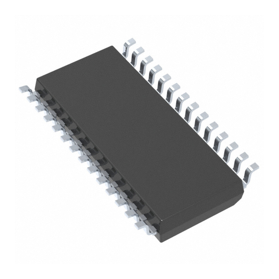
PACKAGE: SO-28
APPLICATIONS
POWER SUPPLY FOR SERVERS AND
WORKSTATIONS
POWER SUPPLY FOR HIGH CURRENT
MICROPROCESSORS
DISTRIBUTED DC-DC CONVERTERS
BLOCK DIAGRAM
PGOOD
VID4
VID3
VID2
VID1
VID0
FBG
FBR
September 2002
OR A
dsON
ROSC / INH
2 PHASE
OSCILLATOR
DIGITAL
VCC
SOFT START
VCCDR
LOGIC
AND
PROTECTIONS
DAC
CH2 OVER
CURRENT
CH1 OVER
CURRENT
10k
10k
IFB
10k
ERROR
AMPLIFIER
REMOTE
BUFFER
10k
VSEN
FB
ORDERING NUMBERS:L6917BD
DESCRIPTION
The device is a power supply controller specifically
designed to provide a high performance DC/DC con-
version for high current microprocessors.
The device implements a dual-phase step-down con-
troller with a 180° phase-shift between each phase.
A precise 5-bit digital to analog converter (DAC) al-
lows adjusting the output voltage from 1.100V to
1.850V with 25mV binary steps.
The high precision internal reference assures the se-
lected output voltage to be within ±0.8%. The high
peak current gate drive affords to have fast switching
to the external power mos providing low switching
losses.
The device assures a fast protection against load
over current and load over/under voltage. An internal
crowbar is provided turning on the low side mosfet if
an over-voltage is detected. In case of over-current,
the system works in Constant Current mode.
SGND
VCCDR
PWM1
-
+
CH 1 OVER
CURRENT
CURRENT
+
READING
TOTAL
CURRENT
AVG
CURRENT
CURRENT
< >
READING
CH 2 OVER
CURRENT
+
-
PWM2
Vcc
COMP
Vcc
L6917B
SO-28
L6917BDTR (Tape & Reel)
BOOT1
UGATE1
HS
PHASE1
LGATE1
LS
ISEN1
PGNDS1
PGND
PGNDS2
ISEN2
LGATE2
LS
PHASE2
UGATE2
HS
BOOT2
1/33
Advertisement

Subscribe to Our Youtube Channel
Related Manuals for ST L6917BD


Summary of Contents for ST L6917BD
- Page 1 ULTRA FAST LOAD TRANSIENT RESPONSE INTEGRATED HIGH CURRENT GATE DRIVERS: UP TO 2A GATE CURRENT SO-28 TTL-COMPATIBLE 5 BIT PROGRAMMABLE ORDERING NUMBERS:L6917BD OUTPUT COMPLIANT WITH VRM 9.0 L6917BDTR (Tape & Reel) 0.8% INTERNAL REFERENCE ACCURACY 10% ACTIVE CURRENT SHARING ACCURACY...
-
Page 2: Absolute Maximum Ratings
L6917B ABSOLUTE MAXIMUM RATINGS Symbol Parameter Value Unit Vcc, V to PGND CCDR Boot Voltage BOOT PHASE UGATE1 PHASE1 UGATE2 PHASE2 LGATE1, PHASE1, LGATE2, PHASE2 to PGND -0.3 to Vcc+0.3 All other pins to PGND -0.3 to 7 Sustainable Peak Voltage t < 20ns @ 600kHz phase THERMAL DATA Symbol... -
Page 3: Electrical Characteristics
L6917B ELECTRICAL CHARACTERISTICS = 12V ±10%, T = 0 to 70°C unless otherwise specified Symbol Parameter Test Condition Unit Vcc SUPPLY CURRENT Vcc supply current HGATEx and LGATEx open 12.5 =12V CCDR BOOT supply current LGATEx open; V =12V CCDR CCDR CCDR Boot supply current... - Page 4 L6917B ELECTRICAL CHARACTERISTICS (continued) = 12V ±10%, T = 0 to 70°C unless otherwise specified Symbol Parameter Test Condition Unit Input Offset FBR=1.100V to1.850V; FBG=GND Slew Rate VSEN=10pF V/µs DIFFERENTIAL CURRENT SENSING µA Bias Current Iload=0 ISEN1 ISEN2 µA Bias Current PGNDSx µA Bias Current at...
- Page 5 L6917B Table 1. VID Settings VID4 VID3 VID2 VID1 VID0 Output Voltage (V) OUTPUT OFF 1.100 1.125 1.150 1.175 1.200 1.225 1.250 1.275 1.300 1.325 1.350 1.375 1.400 1.425 1.450 1.475 1.500 1.525 1.550 1.575 1.600 1.625 1.650 1.675 1.700 1.725 1.750 1.775...
-
Page 6: Pin Function
L6917B PIN FUNCTION Name Description LGATE1 Channel 1 low side gate driver output. VCCDR Mosfet driver supply. It can be varied from 5V to 12V. PHASE1 This pin is connected to the source of the upper mosfet and provides the return path for the high side driver of channel 1. - Page 7 L6917B PIN FUNCTION (continued) Name Description ISEN2 Channel 2 current sense pin. The output current may be sensed across a sense resistor or across the low-side mosfet Rds This pin has to be connected to the low-side mosfet drain or to the sense resistor through a resistor Rg in order to program the positive current limit at 140% as follow: 35 µA R...
- Page 8 L6917B Device Description The device is an integrated circuit realized in BCD technology. It provides complete control logic and protections for a high performance dual-phase step-down DC-DC converter optimized for microprocessor power supply. It is designed to drive N Channel MOSFETs in a dual-phase synchronous-rectified buck topology. A 180 deg phase shift is provided between the two phases allowing reduction in the input capacitor current ripple, reducing also the size and the losses.
- Page 9 L6917B Digital to Analog Converter The built-in digital to analog converter allows the adjustment of the output voltage from 1.100V to 1.850V with 25mV as shown in the previous table 1. The internal reference is trimmed to ensure the precision of 0.8% and a zero temperature coefficient around 70°C.
- Page 10 L6917B Driver Section The integrated high-current drivers allow using different types of power MOS (also multiple MOS to reduce the RDSON), maintaining fast switching transition. The drivers for the high-side mosfets use BOOTx pins for supply and PHASEx pins for return. The drivers for the low-side mosfets use VCCDRV pin for supply and PGND pin for return.
- Page 11 L6917B which the low-side mosfet is on (OFF Time). During this time, the reaction keeps the pin ISENx and PGNDSx at the same voltage while during the time in which the reading circuitry is off, an internal clamp keeps these two pins at the same voltage sinking from the ISENx pin the necessary current.
- Page 12 L6917B current (I >35µA): the device enters in Quasi-Constant-Current operation. The low-side mosfets stays ON INFOx until I becomes lower than 35µA skipping clock cycles. The high side mosfets can be turned ON with a T INFO imposed by the control loop at the next available clock cycle and the device works in the usual way until another OCP event is detected.
- Page 13 L6917B Integrated Droop Function The device uses a droop function to satisfy the requirements of high performance microprocessors, reducing the size and the cost of the output capacitor. This method "recovers" part of the drop due to the output capacitor ESR in the load transient, introducing a de- pendence of the output voltage on the load current As shown in figure 6, the ESR drop is present in any case, but using the droop function the total deviation of the output voltage is minimized.
- Page 14 L6917B Output Voltage Protection and Power Good The output voltage is monitored by pin VSEN. If it is not within +12/-10% (typ.) of the programmed value, the powergood output is forced low. Power good is an open drain output and it is enabled only after the soft start is finished (2048 clock cycles after start-up).
- Page 15 L6917B The power dissipated by the input capacitance is then equal to: ⋅ RM S RM S Input capacitor is designed in order to sustain the ripple relative to the maximum load duty cycle. To reach the high rms value needed by the CPU power supply application and also to minimize components cost, the input capacitance is realized by more than one physical capacitor.
-
Page 16: Main Control Loop
L6917B voltage, during the removal it is discharged only by the output voltage. The following expressions give approx- imate response time for ∆I load transient in case of enough fast compensation network response: ⋅ I ∆ ⋅ I ∆ ----------------------------- - -------------- - a pplic atio n rem ov al... - Page 17 L6917B Current Sharing (CS) Control Loop Active current sharing is implemented using the information from Tran conductance differential amplifier in an average current mode control scheme. A current reference equal to the average of the read current (I ) is internally built;...
- Page 18 L6917B – Z (s) is the compensation network impedance; – Z (s) is the parallel of the two inductor impedance; – A(s) is the error amplifier gain; ∆ ⋅ – -- - ------------------ - · is the ACM PWM transfer function where DVosc is the oscillator ramp amplitude ∆...
-
Page 19: Layout Guidelines
L6917B ⋅ ⋅ ∆ -- - O SC ---------------------------------- ω ⋅ ⋅ ⋅ ------------------------------------------------------- - -- - ------------------- - ⋅ DROOP LAYOUT GUIDELINES Since the device manages control functions and high-current drivers, layout is one of the most important things to consider when designing such high current applications. - Page 20 L6917B as well as for the voltage spikes generated by the distributed inductance along the copper traces are so mini- mized. In fact, the further the mosfet is from the device, the longer is the interconnecting gate trace and as a conse- quence, the higher are the voltage spikes corresponding to the gate pwm rising and falling signals.
-
Page 21: Application Examples
L6917B pins to the load in order to compensate losses along the output power traces and also to avoid the pick-up of any common mode noise. Connecting these pins in points far from the load will cause a non-optimum load reg- ulation, increasing output tolerance. - Page 22 L6917B Figure 16. Demo Board Schematic GNDin C9,C10 C11..C13 VCCDR GNDcc BOOT1 BOOT2 UGATE1 UGATE2 PHASE1 PHASE2 VoutCORE C14, LGATE1 LGATE2 GNDCORE ISEN1 ISEN2 PGNDS1 L6917B PGNDS2 PGND VID4 PGOOD PGOOD VID3 VSEN VID2 VID1 VID0 OSC / INH SGND COMP Several jumpers allow setting different configurations for the device: JP3, JP4 and JP5 allow configuring the remote buffer as desired.
- Page 23 L6917B – Single Supply: In this case JP6 has to be completely shorted. The device is supplied with the same rail that is used for the conversion. With an additional zener diode DZ1 a lower voltage can be derived to supply the mosfets driver if Logic level mosfet are used.
- Page 24 L6917B PCB and Components Layouts Figure 20. PCB and Components Layouts Component Side Internal PGND Plane Figure 21. PCB and Components Layouts Internal SGND Plane Solder Side 24/33...
- Page 25 L6917B CPU Power Supply: 5 to 12V ; 1.7V ; 45A Considering the high slope for the load transient, a high switching frequency has to be used. In addition to fast reaction, this helps in reducing output and input capacitor. Inductance value is also reduced. A switching frequency of 200kHz for each phase is then considered allowing large bandwidth for the compen- sation network.
- Page 26 L6917B Part List SMD 0805 R2, R20 Not Mounted SMD 0805 R3, R4, R5, R6 5.1k SMD 0805 1.43k SMD 0805 6.2k SMD 0805 82Ω SMD 0805 R12 to R16, R19 2.2Ω SMD 0805 R17, R18 0Ω SMD 0805 SMD 0805 C3, C4 100n SMD 0805...
- Page 27 L6917B CPU Power Supply: 12V - VRM 9.0 - 50A thermal Figure 23 shows the device in a high current CPU core power supply solution. The output voltage can be adjusted with binary step from 1.100V to 1.850V following VRM 9.0 specifications. The demo board assembled with the following part list is capable to deliver up to 50A in open air without any kind of airflow.
- Page 28 L6917B Part List (continued) SMD 0805 C3, C4 100n Ceramic SMD 0805 C5, C6, C7, C8 1µ Ceramic SMD 1206 C9, C10 10µ Ceramic SMD 1206 C11 to C13 1800µ/ 16V Rubycon MBZ Radial 10x10.5 C14 to C23 2200µ/ 6.3V Rubycon MBZ Radial 10x10.5 SMD 0805...
- Page 29 L6917B Current Sharing Figure 25 shows the current balancing between the two phases for different values of output current. Figure 25. Load Transient Response Figure 26 shows the system response from 0 to 50A load transient. To obtain such a response, 5 additional capacitors have been added to the output filter to reproduce the motherboard output filter.
- Page 30 L6917B High Current DC-DC: 12V - 3.3 (or 5V) OUT - 35A Figure 27 shows the device in a high current server power supply application. Adding an external resistor divider after the remote sense buffer gives the possibility to increase the regulated voltage.
- Page 31 L6917B Part List SMD 0805 R2, R9 Not Mounted SMD 0805 R3, R6 1.3k SMD 0805 R4, R5 SMD 0805 SMD 0805 SMD 0805 SMD 0805 R12 to R15 SMD 0805 R16, R17, R18 SMD 0805 SMD 0805 SMD 0805 1.3M SMD 0805 Not Mounted...
- Page 32 L6917B inch OUTLINE AND DIM. MECHANICAL DATA MIN. TYP. MAX. MIN. TYP. MAX. 2.65 0.104 0.004 0.012 0.35 0.49 0.014 0.019 0.23 0.32 0.009 0.013 0.020 45° (typ.) 17.7 18.1 0.697 0.713 10.65 0.394 0.419 1.27 0.050 16.51 0.65 0.291 0.299 1.27 0.016...
- Page 33 This publication supersedes and replaces all information previously supplied. STMicroelectronics products are not authorized for use as critical components in life support devices or systems without express written approval of STMicroelectronics. The ST logo is a registered trademark of STMicroelectronics ® 2002 STMicroelectronics - All Rights Reserved...
Need help?
Do you have a question about the L6917BD and is the answer not in the manual?
Questions and answers