Table of Contents
Advertisement
Quick Links
Introduction
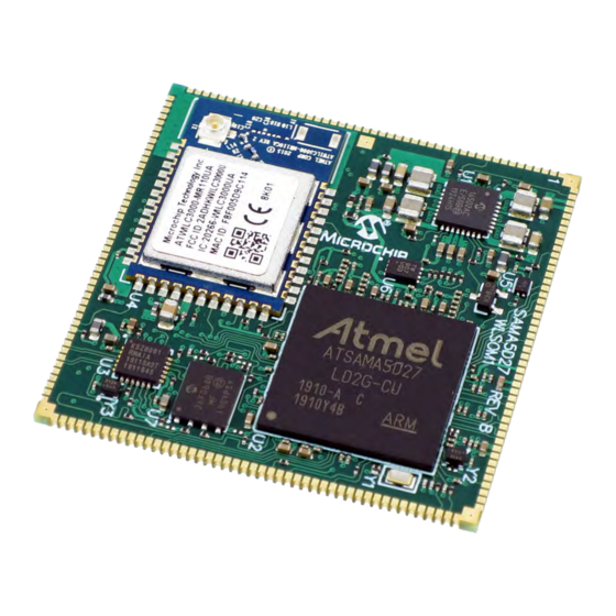
The Microchip SAMA5D27 Wireless System-On-Module 1 (ATSAMA5D27-WLSOM1) is a small single-sided
SOM based on the high-performance System-in-Package (SiP) 32-bit Arm
SAMA5D27, 2 Gb LPDDR2-SDRAM running up to 500 MHz, and Wi-Fi
module.
The ATSAMA5D27-WLSOM1 is built on a common set of proven Microchip components to reduce time to market by
simplifying hardware design and software development.
The ATSAMA5D27-WLSOM1 also limits design rules of the main application board, reducing overall PCB complexity
and cost. The ATSAMA5D27-WLSOM1 is delivered with a free Linux
Figure 1. ATSAMA5D27-WLSOM1 Overview
©
2021 Microchip Technology Inc.
and its subsidiaries
SAMA5D27 Wireless SOM1
ATSAMA5D27-WLSOM1
Complete Datasheet
®
®
Cortex
-A5 processor-based MPU
®
®
plus Bluetooth
(Wi-Fi/BT) Wireless
®
distribution and bare metal C examples.
DS60001590D-page 1
Advertisement
Table of Contents

Related Manuals for Microchip Technology SAMA5D27


Summary of Contents for Microchip Technology SAMA5D27
-
Page 1: Introduction
SAMA5D27 Wireless SOM1 ATSAMA5D27-WLSOM1 Introduction The Microchip SAMA5D27 Wireless System-On-Module 1 (ATSAMA5D27-WLSOM1) is a small single-sided ® ® SOM based on the high-performance System-in-Package (SiP) 32-bit Arm Cortex -A5 processor-based MPU ® ® SAMA5D27, 2 Gb LPDDR2-SDRAM running up to 500 MHz, and Wi-Fi... -
Page 2: Features
SAMA5D27 Wireless SOM1 Features • System-In-Package (ATSAMA5D27C-LD2G-CU) Including: ® ® – Arm Cortex -A5 processor-based SAMA5D27 MPU – 2 Gbit LPDDR2-SDRAM • On-Board Power Management Unit (MCP16502AC-E/S8B) ™ ™ • 64 Mb Serial Quad I/O Flash Memory (SST26VF064BEUIT-104I/MF) with Embedded EUI-48... -
Page 3: Table Of Contents
SAMA5D27 Wireless SOM1 Table of Contents Introduction..............................1 Features................................. 2 Applications..............................2 Reference Documents..........................5 Block Diagram............................6 Pinout ..............................7 3.1. Pinout Overview........................... 7 3.2. Pin List............................7 Functional Description...........................21 4.1. MPU and Memory Subsystem....................21 4.2. Power Management........................25 4.3. LAN Subsystem..........................30 4.4. - Page 4 SAMA5D27 Wireless SOM1 10. Revision History............................ 67 10.1. Rev. D - 08/2021........................67 10.2. Rev. C - 03/2021........................67 10.3. Rev. B - 12/2019.........................68 10.4. Rev. A - 10/2019.........................68 The Microchip Website..........................69 Product Change Notification Service......................69 Customer Support............................69 Product Identification System........................70 Microchip Devices Code Protection Feature....................
-
Page 5: Reference Documents
SAMA5D27 Wireless SOM1 Reference Documents Reference Documents The following reference data sheets are available on www.microchip.com: Table 1-1. Reference Data Sheets Document Title Available KSZ8081RNA/RND www.microchip.com/wwwproducts/en/KSZ8081 SAMA5D2 SIP www.microchip.com/wwwproducts/en/ATSAMA5D27C-LD2G SST26VF064BEUI www.microchip.com/wwwproducts/en/SST26VF064BEUI MCP16502 https://www.microchip.com/wwwproducts/en/MCP16502 MIC841/2 https://www.microchip.com/wwwproducts/en/MIC842 DSC60XXB www.microchip.com/wwwproducts/en/DSC6000B DSC61XXB www.microchip.com/wwwproducts/en/DSC6100B ATWILC3000-MR110UA https://www.microchip.com/wwwproducts/en/ATWILC3000 ATECC608B-TNGTLS www.microchip.com/wwwproducts/en/ATECC608B-TNGTLS... -
Page 6: Block Diagram
SAMA5D27 Wireless SOM1 Block Diagram Block Diagram The following figure shows the block diagram of the ATSAMA5D27-WLSOM1 module. Figure 2-1. ATSAMA5D27-WLSOM1 Module Block Diagram 3.3V 1.8V VDDFUSE VDDISC VDDANA VDDBU 600mA 900mA MAIN Voltage Monitor MIC842NYMT 64 Mbit Serial Quad I/O 3.0-5.5V... -
Page 7: Pinout
3 - VDD_MAIN COMPP - 139 COMPN - 140 2 - VDD_MAIN GND - 141 1 - GND Pin List The following tables provide the SAMA5D27-WLSOM1 module pin description. Complete Datasheet DS60001590D-page 7 © 2021 Microchip Technology Inc. and its subsidiaries... - Page 8 SAMA5D27 Wireless SOM1 Pinout Important: Compared to SAMA5D2 Series devices, some PIO features are not listed. These features are used internally on the SAMA5D27-WLSOM1 and cannot be shared with other PIOs for use with features or for signal integrity. 3.2.1 PIOA Pin Description Table 3-1. PIOA Pin Description...
- Page 9 SAMA5D27 Wireless SOM1 Pinout ...continued Primary Alternate PIO Peripheral Note Pad No. Power Rail I/O Type Reset State (Signal, Dir, PU, PD, HiZ, ST) Signal Dir Signal Dir Func Signal Dir IO Set SDMMC0_DAT6 QSPI1_IO1 VDDSDHC GPIO_EMMC – – TCLK5...
- Page 10 SAMA5D27 Wireless SOM1 Pinout ...continued Primary Alternate PIO Peripheral Note Pad No. Power Rail I/O Type Reset State (Signal, Dir, PU, PD, HiZ, ST) Signal Dir Signal Dir Func Signal Dir IO Set SPI0_MISO VDD_3V3 GPIO_IO PA16 – – PIO, I, PU, ST...
- Page 11 SAMA5D27 Wireless SOM1 Pinout ...continued Reset State (Signal, Dir, PU, PD, HiZ, Pad No. Power Rail I/O Type Primary Alternate PIO Peripheral Note Signal Dir Signal Dir Func Signal Dir IO Set TCLK2 VDD_3V3 GPIO_QSPI – – PWMH2 PIO, I, PU, ST...
- Page 12 SAMA5D27 Wireless SOM1 Pinout ...continued Reset State (Signal, Dir, PU, PD, HiZ, Pad No. Power Rail I/O Type Primary Alternate PIO Peripheral Note Signal Dir Signal Dir Func Signal Dir IO Set FLEXCOM0_IO2 I/O VDD_3V3 GPIO PB30 – – TCLK5...
- Page 13 SAMA5D27 Wireless SOM1 Pinout ...continued Primary Alternate PIO Peripheral Note Pad No. Power Rail I/O Type Reset State (Signal, Dir, PU, PD, HiZ, ST) Signal Dir Signal Dir Func Signal Dir IO Set TCLK1 SPI1_NPCS1 VDD_3V3 GPIO – – PIO, I, PU, ST...
- Page 14 SAMA5D27 Wireless SOM1 Pinout ...continued Primary Alternate PIO Peripheral Note Pad No. Power Rail I/O Type Reset State (Signal, Dir, PU, PD, HiZ, ST) Signal Dir Signal Dir Func Signal Dir IO Set LCDDAT7 ISI_D6 VDDISC GPIO PC15 – –...
- Page 15 SAMA5D27 Wireless SOM1 Pinout ...continued Primary Alternate PIO Peripheral Note Pad No. Power Rail I/O Type Reset State (Signal, Dir, PU, PD, HiZ, ST) Signal Dir Signal Dir Func Signal Dir IO Set LCDDAT20 VDDISC GPIO_CLK PC24 – – ISI_MCK...
- Page 16 SAMA5D27 Wireless SOM1 Pinout 3.2.4 PIOD Pin Description Primary Alternate PIO Peripheral Note Pad No. Power Rail I/O Type Reset State (Signal, Dir, PU, PD, HiZ, ST) Signal Dir Signal Dir Func Signal Dir IO Set LCDPCK FLEXCOM4_IO4 VDD_3V3 GPIO_CLK –...
- Page 17 SAMA5D27 Wireless SOM1 Pinout ...continued Primary Alternate PIO Peripheral Note Pad No. Power Rail I/O Type Reset State (Signal, Dir, PU, PD, HiZ, ST) Signal Dir Signal Dir Func Signal Dir IO Set GTX3 VDDANA GPIO_AD I/O PTC_ROW5 – PIO, I, PU, ST...
- Page 18 SAMA5D27 Wireless SOM1 Pinout ...continued Primary Alternate PIO Peripheral Note Pad No. Power Rail I/O Type Reset State (Signal, Dir, PU, PD, HiZ, ST) Signal Dir Signal Dir Func Signal Dir IO Set VDDANA GPIO_AD PD17 PTC_COL6 – GMDC PIO, I, PU, ST...
- Page 19 SAMA5D27 Wireless SOM1 Pinout ...continued Pin No. Pin Name Power Rail Description USBA_P VDD_3V3 USB Device High-Speed Data + HSIC_STROBE VDDHSIC (1.2V) USB High-Speed Inter-Chip Strobe HSIC_DATA VDDHSIC (1.2V) USB High-Speed Inter-Chip Data USBB_N VDD_3V3 USB Host Port B High-Speed Data -...
- Page 20 SAMA5D27 Wireless SOM1 Pinout ...continued Pin No. Pin Name Power Rail Type Description VDDBU VDDBU Backup Voltage Input VDDFUSE VDDFUSE VDDFUSE Voltage Input VDDISC VDDISC VDDISC Voltage Input 2, 3, 4 VDD_MAIN VDD_MAIN Main Input Voltage 12, 13 VDD_3V3 VDD_3V3 3.3V Voltage Output...
-
Page 21: Functional Description
MPU and Memory Subsystem 4.1.1 SAMA5D27 System-In-Package The SAMA5D27 System-In-Package (SiP) (ATSAMA5D27C-LD2G-CU) integrates the ARM Cortex-A5 processor- based SAMA5D2 MPU with 2 Gbit LPDDR2-SDRAM in a single package. By combining the high-performance, ultra-low power SAMA5D2 with LPDDR2-SDRAM in a single package, PCB routing complexity, area and number of layers is reduced. - Page 22 SAMA5D27 Wireless SOM1 Functional Description Figure 4-2. SAMA5D27 SiP Decoupling Schematic VDDIODDR VDDCORE SAMA5D27C-LD2G-CU 0402 4.7uF SAMA5D27C-LD2G-CU 0402 4.7uF 0402 4.7uF DDRM_VDD12 DDRM_VSS 0402 4.7uF 0201 0.1uF DDRM_VDD12 DDRM_VSS VDDCORE GNDCORE 0402 4.7uF 0201 0.1uF DDRM_VDD12 DDRM_VSS VDDCORE GNDCORE 0201 0.1uF 0201 0.1uF...
- Page 23 SAMA5D27 Wireless SOM1 Functional Description Figure 4-3. Power Management Unit Schematic VDD_MAIN 100k 0201 BSS138 PIOBU0_PMIC MCP16502AC-E/S8B VDD_MAIN VDDUTMII (3V3) 180R PVIN1 BLM18PG181SN1D 4.7uF 4.7uF 0201 0402 SHDN PWRHLD PGND1 0402 0201 VDD_3V3 22uF VDDOSC_PLL (3V3) 1.5uH 0603 2.2R 10uH nSTART_SOM...
- Page 24 SAMA5D27 Wireless SOM1 Functional Description Figure 4-4. QSPI Memory Schematic VDD_3V3 0201 0201 0201 0201 0201 0201 VDD_3V3 SI/SIO0 QSPI1_IO0_PB7 SO/SIO1 QSPI1_IO1_PB8 WP/SIO2 0.1uF QSPI1_IO2_PB9 HOLD/SIO3 6.3V QSPI1_IO3_PB10 0201 QSPI1_SCK_PB5 TPAD SST26VF064BEUIT-104I/MF SCK_QSPI_PB5 SIO3_QSPI_PB10 SIO2_QSPI_PB9 SIO1_QSPI_PB8 SIO0_QSPI_PB7 NCS_QSPI 4.1.3.2 MAC Address The SST26VF064BEUI is pre-programmed at the factory with globally unique EUI-48 and EUI-64 node identifiers.
-
Page 25: Power Management
SAMA5D2 processor and on-board components. The PMIC on-board switching regulators generate the 3.3V, 1.20V, 1.25V and 1.8V voltage supplies required by the SAMA5D27 processor and on-board components. The ATSAMA5D27-WLSOM1 delivers external power supplies to the main board application, such as VDD_DDR (1.8V with 900 mA current capability), VDD_3V3 (3.3V with 600mA output current capability) and VLDO2 output... - Page 26 SAMA5D27 Wireless SOM1 Functional Description 4.2.2 Various Power Configurations Two different configurations are described below, depending on customer use. • Single Supply—ATSAMA5D27-WLSOM1 can be supplied by only one input supply (for example, a 5V AC/DC wall adapter) and other input supplies can be connected to the internal 3.3V regulator VDD_3V3. All the PIO lines are supplied at 3.3V.
- Page 27 SAMA5D27 Wireless SOM1 Functional Description 4.2.2.2 Power Configurations: Multiple Supplies Figure 4-8. ATSAMA5D27-WLSOM1 Multiple Supplies Connection Example Backup VDDBU Battery VDD_3V3 VDDISC (2.5V/2.8V/3.0V) VDDANA Input Supply VDD_MAIN (3.0V - 5.5V) LDO + Switch VDDSDHC (3.3V/1.8V) Application Fuse VDDFUSE (2.5V) Application Board VDD_DDR (1.8V)
- Page 28 SAMA5D27 Wireless SOM1 Functional Description 4.2.3.2 Power ON/OFF Sequences for Single Supply Figure 4-9. ATSAMA5D27-WLSOM1 Single Supply Connection: Power-On Sequence SYSTEM STATUS STARTUP POWER-UP NRST RELEASED SYSTEM BOOT I²C COMMAND VLDO2 POWER UP VDD_MAIN 5.0V nSTART_SOM VDD_3V3 VDDBU VDDANA VDDISC VDDSDHC...
- Page 29 SAMA5D27 Wireless SOM1 Functional Description 4.2.3.3 Power ON/OFF Sequences for Multiple Supplies Figure 4-11. ATSAMA5D27-WLSOM1 Multiple Supplies Connections: Power-On Sequence SYSTEM STATUS BACKUP STARTUP POWER-UP NRST RELEASED SYSTEM BOOT I²C COMMAND VLDO2 POWER UP VDDBU 1.65V TO 3.6V VDD_MAIN 5.0V nSTART_SOM...
-
Page 30: Lan Subsystem
SAMA5D27 Wireless SOM1 Functional Description Figure 4-13. Baseboard Power Delivery Application Diagram Example (3.3V) VDD_3V3 VDDSDHC (3.3V / 1.8V) REGULATOR SD-CARD MIC5353YMT DC/DC VDDANA DCIN CONVERTER (5.0V) VDDIN (12V) 1V8 Output MIC24051 SHDN VLDO2 VDDISC (1.8V-3.3V) (2.5V) REGULATOR CAMERA MIC5259-2.5YD5 WLSOM1... -
Page 31: Voltage Threshold Detector
SAMA5D27 Wireless SOM1 Functional Description Figure 4-15. Ethernet Phy Schematic Example DIFF100 ETH_TX_P DIFF100 ETH_TX_N DIFF100 ETH_RX_P DIFF100 ETH_RX_N ATSAMA5D27-WLSOM1 0.1uF 0.1uF 0402 0402 Green 120R Right GND_ETH 0402 Yellow BLM18PG121SN1D VDD_3V3 470R 0402 Lift EARTH_ETH GND_ETH ETH_LED0 CON RJ-45 JD2-0010NL... -
Page 32: Radio Subsystem
SAMA5D27 Wireless SOM1 Functional Description The MIC842 incorporates a voltage reference and comparator with fixed internal hysteresis; two external resistors are used to set the switching threshold voltage. Supply current is extremely low (1.5 μA, typical), making it ideal for portable applications. -
Page 33: External Interfaces
SAMA5D27 Wireless SOM1 Functional Description The ATWILC3000-MR110UA utilizes highly -optimized 802.11 Bluetooth coexistence protocols. The only external clock sources needed are a high-speed crystal or oscillator and a 32.768 kHz clock for sleep operation. In the ATSAMA5D27-WLSOM1, the 32.768 kHz clock is provided by the ATSAMA5D27 through PB13. - Page 34 SAMA5D27 Wireless SOM1 Functional Description Figure 4-19. 4-bit/8-bit SD Card Power Switch Example Schematic VDD_1V8 VDD_3V3 VDDSDHC 0.1uF PA11 ADG849 ATSAMA5D27-WLSOM1 Figure 4-20. 4-bit SD Card Interface Example Schematic VDDSDHC VDD_3V3 0.1uF 4.7uF 0402 1% DAT3 0402 1% VSS1 VSS2 0402 1%...
- Page 35 SAMA5D27 Wireless SOM1 Functional Description Figure 4-21. 8-bit SD Card Interface Example Schematic VDDSDHC VDD_3V3 0.1uF 4.7uF 0402 1% DAT3 0402 1% VSS1 0402 1% DAT0 0402 1% DAT1 DAT7 0402 1% DAT2 DAT6 PA13 DAT5 PA12 DAT4 SHIELD 0402 1%...
- Page 36 SAMA5D27 Wireless SOM1 Functional Description Figure 4-23. EMI Improvement Layout Example TOP LAYER INNER LAYER 4.6.2 Interfacing with e-MMC The Secure Digital Multimedia Card (SDMMC) Controller supports the Embedded MultiMedia Card (e-MMC) Specification V4.41, the SD Memory Card Specification V3.0, and the SDIO V3.0 specification. It is compliant with the SD Host Controller Standard V3.0 specification.
- Page 37 SAMA5D27 Wireless SOM1 Functional Description Figure 4-25. e-MMC Interface Example Schematic VDD_3V3 VDDSDHC VDDSDHC 0.1uF 2.2uF 0.1uF 2.2uF DAT0 DAT1 DAT2 DAT3 DAT4 DAT5 DAT6 DAT7 PA10 nRST ATSAMA5D27-WLSOM1 4.6.2.2 Design Layout Recommendations When designing the e-MMC interface, consider the following recommendations: •...
- Page 38 SAMA5D27 Wireless SOM1 Functional Description In order to improve the overall system performance, the DATA phase of the transfer can be DMA-assisted. 4.6.3.1 Design Schematic Example The example below is given with an 8-bit NAND Flash memory from Micron. Figure 4-27. NAND Flash Interface Example Schematic...
- Page 39 SAMA5D27 Wireless SOM1 Functional Description compression, programmable color space conversion and horizontal and vertical chrominance subsampling module. The module also integrates a triple channel Direct Memory Access Controller host interface. 4.6.4.1 Design Schematic Example The example schematics shown below are for different Image Sensor supply voltages.
- Page 40 SAMA5D27 Wireless SOM1 Functional Description • Place data signals at least 2 times the trace width away from any copper plan. Figure 4-31. ISC Layout Example Copper Plane Data Traces Clock Trace Data Traces 4.6.4.3 EMI Improvement Recommendations To reduce radiation emission, consider the following recommendations: •...
- Page 41 SAMA5D27 Wireless SOM1 Functional Description The Serial Peripheral Interface is essentially a shift register that serially transmits data bits to other SPI devices. During a data transfer, one SPI system acts as the “host”' which controls the data flow, while the other devices act as “clients'' which have data shifted into and out by the host.
- Page 42 SAMA5D27 Wireless SOM1 Functional Description Table 4-6. FLEXCOM Interfaces Configurations in SPI Mode Interface Instance IO set Pin # Pin Name Comments FLEXCOM0 PB28 FLEXCOM0_IO0 MOSI Signal FLEXCOM0 PB29 FLEXCOM0_IO1 MISO Signal FLEXCOM0 PB30 FLEXCOM0_IO2 SPCK Signal FLEXCOM0 PB31 FLEXCOM0_IO3 NPCS0 Signal...
- Page 43 SAMA5D27 Wireless SOM1 Functional Description The Two-wire Interface (TWI) interconnects components on a unique two-wire bus, made up of one clock line and one data line with speeds of up to 400 kbit/s in Fast mode and up to 3.4 Mbit/s in High-Speed Client mode only, based on a byte-oriented transfer format.
- Page 44 SAMA5D27 Wireless SOM1 Functional Description Figure 4-33. CLASS-D Interface Example Schematic MAIN_VOLT (Up to 12V) 10uF 10uF 10uF 10uF 1N4148W 10000pF SSM3J56ACT SSM3K56ACT CLASSD_R0 CLASSD_R1 CLASSD_R2 0402 CLASSD_R3 BLM18PG181SN1D ATSAMA5D27-WLSOM1 TERMINAL 1x4 BLM18PG181SN1D 1N4148W 10000pF SSM3J56ACT SSM3K56ACT ® 4.6.8 QTouch Peripheral Touch Controller (PTC)
- Page 45 SAMA5D27 Wireless SOM1 Functional Description Figure 4-34. LCD Schematic Example LCD_ID_PC09 0402 1% LCD_D2_PC10 PC10 0402 1% LCD_D3_PC11 PC11 0402 1% LCD_D4_PC12 PC12 0402 1% LCD_D5_PC13 PC13 0402 1% LCD_D6_PC14 PC14 0402 1% LCD_D7_PC15 PC15 0402 1% LCD_D10_PC16 PC16 0402 1%...
- Page 46 SAMA5D27 Wireless SOM1 Functional Description Figure 4-35. LCD Layout Example Copper Plane Data Traces Clock Trace Data Traces 4.6.9.3 EMI Improvement Recommendations To reduce radiation emission, consider the following recommendations: • Position the LCD bus interface in inner layers of the PCB.
- Page 47 SAMA5D27 Wireless SOM1 Functional Description Figure 4-36. EMI Improvement Layout Example LCD_ID_PC09 PC09 0402 1% LCD_D2_PC10 PC10 0402 1% LCD_D3_PC11 PC11 0402 1% LCD_D4_PC12 PC12 0402 1% LCD_D5_PC13 PC13 0402 1% LCD_D6_PC14 PC14 0402 1% LCD_D7_PC15 PC15 0402 1% LCD_D10_PC16 PC16...
-
Page 48: Electrical Characteristics
SAMA5D27 Wireless SOM1 Electrical Characteristics Electrical Characteristics Absolute Maximum Ratings Stresses beyond those listed under “Absolute Maximum Ratings” may cause permanent damage to the device. This is a stress rating only and functional operation of the device at these or other conditions beyond those indicated in the operational sections of this specification is not implied. -
Page 49: Power Consumption
SAMA5D27 Wireless SOM1 Electrical Characteristics ...continued Parameters Conditions Min. Typ. Max. Unit Low-level Input Current All GPIO @ 3.3V – µA High-level Input Current All GPIO @ 3.3V – µA All GPIO @ 3.3V / Low – – Low-level Output Current All GPIO @ 3.3V / High... - Page 50 SAMA5D27 Wireless SOM1 Electrical Characteristics wpa_cli -iwlan0 -p/var/run/wpa_supplicant set_network 2 key_mgmt WPA-PSK wpa_cli -iwlan0 -p/var/run/wpa_supplicant set_network 2 psk '"12345678"' wpa_cli -iwlan0 -p/var/run/wpa_supplicant select_network 2 udhcpc -iwlan0 & iperf -s -i 1 -w 512k & (At WLSOM terminal) iperf -c 192.168.1.3 -i 1 -t 300 -w 512k (At PC terminal) For Ethernet activity ping 192.168.1.2 &...
-
Page 51: Radio Performance
SAMA5D27 Wireless SOM1 Electrical Characteristics ...continued Scenario N°7 Scenario N°8 Scenario N°9 Scenario N°10 Scenario N°11 Scenario Setup Backup Mode Backup Mode w/ Self refresh ULP0 Mode ULP1 Mode Idle Mode PVDD_MAIN @5V 294.5 µW 413 mW 299 mW 292 mW 293.5 mW... -
Page 52: Mechanical Characteristics
SAMA5D27 Wireless SOM1 Mechanical Characteristics Mechanical Characteristics Module Outline Drawings Figure 6-1. ATSAMA5D27-WLSOM1 Module Drawing PIN 1 CORNER P2Eb TP10 TP11 f x n SAMA5D27-WLSOM1 DIMENSIONS Drawn by : R C R P2Ea Pads : jjj x m SAMA5D27-WLSOM1_POD Body : 40.8 x 40.8 x 3.287... - Page 53 SAMA5D27 Wireless SOM1 Mechanical Characteristics ...continued Common Dimensions Symbol Comments Min. Typ. Max. Opening Drill Diameter – 0.400 – Pad Count – – Test Point Diameter – 1.000 – Test Point Count – – P2Ea – 2.000 – Pad Axis to Edge P2Eb –...
-
Page 54: Module Land Pattern (Host Board Pcb Footprint)
SAMA5D27 Wireless SOM1 Mechanical Characteristics Module Land Pattern (Host Board PCB Footprint) Figure 6-2. ATSAMA5D27-WLSOM1 Land Pattern Drawing LAND PATTERN RECOMMENDATIONS PIN 1 CORNER 10.75 9.75 3.25 1.25 Inside <S1-S2> square, keepout area SAMA5D27-WLSOM1 DIMENSIONS Drawn by : R C R No signals and power vias, no tracks are allowed. -
Page 55: Other Characteristics
SAMA5D27 Wireless SOM1 Mechanical Characteristics Figure 6-3. GND Pads Overview and Layout Recommendation WRONG GOOD Note: It is recommended to use the layout as shown on the right above. This solution increases RF performance of the Wi-Fi and Bluetooth communications and optimizes heat sink capability of the system; on the host board, do not apply thermal brakes on the TOP layout around GND pads. -
Page 56: Assembly And Storage Information
SAMA5D27 Wireless SOM1 Assembly and Storage Information Assembly and Storage Information Storage Condition 7.1.1 Moisture Barrier Bag Before Opening A moisture barrier bag must be stored at a temperature of less than 30°C with humidity under 85% RH. The calculated shelf life for the dry-packed product is 12 months from the date the bag is sealed. -
Page 57: Reflow Profile
SAMA5D27 Wireless SOM1 Assembly and Storage Information Figure 7-1. IPC/JEDEC Table Reflow Profile The ATSAMA5D27-WLSOM1 is assembled using standard lead-free reflow profile IPC/JEDEC J-STD-020E. In addition to the initial assembly solder, we recommend a maximum of two additional soldering processes: •... - Page 58 SAMA5D27 Wireless SOM1 Assembly and Storage Information Figure 7-2. Reflow Profile Example used for Soldering ATSAMA5D27-WLSOM1 Module on ATSAMA5D27- WLSOM1-EK1 Board Supplier T p > T c User T p < T c T c -5°C Supplier t p User t p -5°C...
-
Page 59: Regulatory Approval
SAMA5D27 Wireless SOM1 Regulatory Approval Regulatory Approval The ATSAMA5D27-WLSOM1 is the implementation of the ATWILC3000-MR110UA module in a particular host, in this case the PCB of the ATSAMA5D27-WLSOM1. The ATWILC3000-MR110UA module has received regulatory approval for the following countries: •... -
Page 60: Canada
SAMA5D27 Wireless SOM1 Regulatory Approval This equipment has been tested and found to comply with the limits for a Class B digital device, pursuant to part 15 of the FCC Rules. These limits are designed to provide reasonable protection against harmful interference in a residential installation. -
Page 61: Europe
SAMA5D27 Wireless SOM1 Regulatory Approval User Manual Notice for License-Exempt Radio Apparatus (from Section 8.4 RSS-Gen, Issue 5, April 2018): User manuals for license-exempt radio apparatus shall contain the following or equivalent notice in a conspicuous location in the user manual or alternatively on the device or both: This device contains license-exempt transmitter(s)/receiver(s) that comply with Innovation, Science and Economic Development Canada’s license-exempt RSS(s). - Page 62 SAMA5D27 Wireless SOM1 Regulatory Approval The ATSAMA5D27-WLSOM1 module has been tested to RED 2014/53/EU Essential Requirements for Health and Safety (Article (3.1(a)), Electromagnetic Compatibility (EMC) (Article 3.1(b)), and Radio (Article 3.2) and are summarized in European Compliance Testing. The ETSI provides guidance on modular devices in “Guide to the application of harmonized standards covering articles 3.1b and 3.2 of the Directive 2014/53/EU (RED) to multi-radio and combined radio and non-...
-
Page 63: Approved Antenna Types
8.3.3 Simplified EU Declaration of Conformity Hereby, Microchip Technology Inc. declares that the radio equipment type [ATSAMA5D27-WLSOM1] is in compliance with Directive 2014/53/EU. The full text of the EU declaration of conformity is available at the following internet address : https:// www.microchip.com/wwwproducts/en/ATSAMA5D27-WLSOM1... - Page 64 SAMA5D27 Wireless SOM1 Regulatory Approval Notes: X = Covered under the certification. If the end product using the module is designed to have an antenna port that is accessible to the end user, then a unique (nonstandard) antenna connector (refer to FCC 353028) must be used;...
- Page 65 SAMA5D27 Wireless SOM1 Regulatory Approval Figure 8-1. SAMA5D27-WLSOM1 Antenna Placement 5 cm Preferred Antenna Cable Routing Directions MICROCHIP ATSAMA5D27-WLSOM1 1941000 RevB.0 - 0000027 5 cm Antenna Keep out Area Complete Datasheet DS60001590D-page 65 © 2021 Microchip Technology Inc. and its subsidiaries...
-
Page 66: Ordering Information
SAMA5D27 Wireless SOM1 Ordering Information Ordering Information Table 9-1. Ordering Details Ordering Code Package Description Regulatory Information Certified Microchip MPU Wireless module with ATSAMA5D27-WLSOM1 40.8 x 40.8 x 3.287 mm FCC, ISED, CE SAMA5D27, WILC3000 and U.FL connector Complete Datasheet DS60001590D-page 66 ©... -
Page 67: Revision History
SAMA5D27 Wireless SOM1 Revision History Revision History 10.1 Rev. D - 08/2021 Updated European Compliance Testing. 10.2 Rev. C - 03/2021 Note: Microchip is in the process of implementing inclusive language in our documentation. During this update, you may see the old terms and the new terms in our documentation text. We apologize for any confusion. -
Page 68: Rev. B - 12/2019
SAMA5D27 Wireless SOM1 Revision History 10.3 Rev. B - 12/2019 Updated Figure 3-1. Updated pins 151, 152 in Pin Description: System. Updated figure in 4.1.4 Secure Element. Updated figure in 4.2.1 Power Architecture. Updated 4.3.1 Ethernet Phy. Modified component reference in 4.5 Radio... -
Page 69: The Microchip Website
SAMA5D27 Wireless SOM1 The Microchip Website Microchip provides online support via our website at www.microchip.com/. This website is used to make files and information easily available to customers. Some of the content available includes: • Product Support – Data sheets and errata, application notes and sample programs, design resources, user’s guides and hardware support documents, latest software releases and archived software •... -
Page 70: Product Identification System
Examples: • ATSAMA5D27-WLSOM1 = System-On-Module (SOM) based on the SAMA5D27, with 2 Gb LPDDR2-SDRAM running up to 500 MHz, and a Wi-Fi/BT Wireless module Microchip Devices Code Protection Feature Note the following details of the code protection feature on Microchip devices: •... -
Page 71: Trademarks
The Adaptec logo, Frequency on Demand, Silicon Storage Technology, and Symmcom are registered trademarks of Microchip Technology Inc. in other countries. GestIC is a registered trademark of Microchip Technology Germany II GmbH & Co. KG, a subsidiary of Microchip Technology Inc., in other countries. -
Page 72: Worldwide Sales And Service
Tel: 631-435-6000 Sweden - Stockholm San Jose, CA Tel: 46-8-5090-4654 Tel: 408-735-9110 UK - Wokingham Tel: 408-436-4270 Tel: 44-118-921-5800 Canada - Toronto Fax: 44-118-921-5820 Tel: 905-695-1980 Fax: 905-695-2078 Complete Datasheet DS60001590D-page 72 © 2021 Microchip Technology Inc. and its subsidiaries...
Need help?
Do you have a question about the SAMA5D27 and is the answer not in the manual?
Questions and answers