Table of Contents
Advertisement
Quick Links
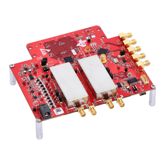
The Texas Instruments TSW308x evaluation module (EVM) provides a basic platform to evaluate the
DAC348x in a complete RF transmit signal chain. Along with the DAC348x, the EVM includes a
LMK04806B clock jitter cleaner and generator source, which provides the clocks required for the DAC and
the external pattern generator. The EVM also includes on-board TRF3705 I/Q modulators, which provide
IF-to-RF upconversion for basic transmitter evaluation. This EVM is ideally suited for mating with the
Texas Instruments TSW1400 pattern generation board for evaluating WCDMA, LTE, or other high-
performance modulation schemes.
...................................................................................................................
1
1.1
1.2
2
2.1
2.2
3
3.1
3.2
3.3
3.4
4
4.1
4.2
4.3
4.4
4.5
5
5.1
5.2
5.3
6
6.1
6.2
1
2
3
4
5
6
7
8
9
Altera is a registered trademark of Altera Corporation.
Xilinx is a registered trademark of Xilinx Inc..
SLAU374B - December 2011 - Revised May 2016
Submit Documentation Feedback
.............................................................................................................
................................................................................................
.............................................................................................................
.............................................................................................
.................................................................................................
...................................................................................
...............................................................................................
..............................................................................
...........................................................................................
...........................................................................
.....................................................................................................
..................................................................................
List of Figures
.............................................................................................
.............................................................................................
...........................................................................................
....................................................................................
............................................................................................................
.................................................................................
................................................................................
..........................................................................................
Copyright © 2011-2016, Texas Instruments Incorporated
SLAU374B - December 2011 - Revised May 2016
TSW308x Evaluation Module
Contents
..........................................................................
.....................................................
..............................................
............................................
...........................................................
........................................................................
..........................................................................
User's Guide
TSW308x Evaluation Module
3
3
4
7
7
7
17
17
17
18
20
24
24
25
26
26
27
28
29
29
29
29
29
29
4
5
6
8
9
10
12
13
15
1
Advertisement
Table of Contents

Related Manuals for Texas Instruments TSW308 Series


Summary of Contents for Texas Instruments TSW308 Series
-
Page 1: Table Of Contents
SLAU374B – December 2011 – Revised May 2016 TSW308x Evaluation Module The Texas Instruments TSW308x evaluation module (EVM) provides a basic platform to evaluate the DAC348x in a complete RF transmit signal chain. Along with the DAC348x, the EVM includes a LMK04806B clock jitter cleaner and generator source, which provides the clocks required for the DAC and the external pattern generator. - Page 2 ..........TSW308x RF Amp / Attenuator Output (TRF3705 Low-Gain Mode) ..........TSW308x RF Amp / Attenuator Output (TRF3705 High-Gain Mode) TSW308x Evaluation Module SLAU374B – December 2011 – Revised May 2016 Submit Documentation Feedback Copyright © 2011–2016, Texas Instruments Incorporated...
-
Page 3: Introduction
The TSW308x evaluation module (EVM) is a family of circuit boards that allow designers to evaluate the performance of the Texas Instruments DAC348x digital-to-analog converters (DAC). The DAC348x family consists of DAC3482, DAC3484, and DAC34H84. The 16-bit, 1.25 GSPS, DAC348x has integrated 2x/4x/8x/16x interpolation filters, 32-bit NCO, on-chip PLL, and exceptional linearity at high IFs. -
Page 4: Evm Block Diagram
DAC3484 PARITY Default TRF3705 Output Splitter (LVDS DC Coupled) TRF3705 Power Supply 6V Only Circuits Figure 1. TSW3084EVM Block Diagram TSW308x Evaluation Module SLAU374B – December 2011 – Revised May 2016 Submit Documentation Feedback Copyright © 2011–2016, Texas Instruments Incorporated... -
Page 5: Tsw3085Evm Block Diagram
SYNC TRF3705 DAC3482 PARITY (LVDS DC Coupled) Default TRF3705 Output Power Supply 6V Only Circuits Figure 2. TSW3085EVM Block Diagram SLAU374B – December 2011 – Revised May 2016 TSW308x Evaluation Module Submit Documentation Feedback Copyright © 2011–2016, Texas Instruments Incorporated... -
Page 6: Tsw30H84Evm Block Diagram
DAC34H84 PARITY Default TRF3705 Output Splitter (LVDS DC Coupled) TRF3705 Power Supply 6V Only Circuits Figure 3. TSW30H84EVM Block Diagram TSW308x Evaluation Module SLAU374B – December 2011 – Revised May 2016 Submit Documentation Feedback Copyright © 2011–2016, Texas Instruments Incorporated... -
Page 7: Software Control
4. Once installed, launch the program by clicking on the TSW308x program in Start>Programs>Texas Instruments DACs>TSW308x. For Windows XP system, the installation directory is located at C:\Program Files\Texas Instruments\TSW308x. For Windows 7 system, it is located at C:\Program Files (x86)\Texas Instruments\TSW308x 5. -
Page 8: Input Tab Control Options - Dac348X
Data Formatter Sync (DAC3482 and DAC3484): Synchronization source for FIFO data formatter. Select between LVDS FRAME or LVDS SYNC signals. TSW308x Evaluation Module SLAU374B – December 2011 – Revised May 2016 Submit Documentation Feedback Copyright © 2011–2016, Texas Instruments Incorporated... -
Page 9: Pll Configuration
– At the top side of the TSW30H84, set SJP9, SJP10, SJP11, and SJP12 to the 2-3 position for approximately 1 inches (160 ps) of trace delay. 2.2.1.3 PLL Settings Figure 5. PLL Configuration SLAU374B – December 2011 – Revised May 2016 TSW308x Evaluation Module Submit Documentation Feedback Copyright © 2011–2016, Texas Instruments Incorporated... -
Page 10: Digital Tab Control Options - Dac348X
Note: If fine mixer (NCO) is used, the Enable Mixer button must be checked, and the coarse mixer must be bypassed. See the following NCO bullet for detail. TSW308x Evaluation Module SLAU374B – December 2011 – Revised May 2016 Submit Documentation Feedback Copyright © 2011–2016, Texas Instruments Incorporated... - Page 11 — SYNC: sync from the external SYNC signal. — SIF SYNC: sync from SIF Sync. Uncheck and check the SIF Sync button for sync event. SLAU374B – December 2011 – Revised May 2016 TSW308x Evaluation Module Submit Documentation Feedback Copyright © 2011–2016, Texas Instruments Incorporated...
-
Page 12: Output Tab Control Options - Dac348X
● Output Shutoff On: allows outputs to shut off when DACCLK GONE, DATACLK GONE, or FIFO COLLISION alarm event occurs. TSW308x Evaluation Module SLAU374B – December 2011 – Revised May 2016 Submit Documentation Feedback Copyright © 2011–2016, Texas Instruments Incorporated... -
Page 13: Lmk04800 Tab Control Options
PLL mode, this becomes the reference clock input for the PLL block. • CLK8: TSW1400/TSW3100 FPGA input clock. This clock type is AC coupled LVDS. The clock rate SLAU374B – December 2011 – Revised May 2016 TSW308x Evaluation Module Submit Documentation Feedback Copyright © 2011–2016, Texas Instruments Incorporated... - Page 14 Clicking on the Advance Settings tab at the bottom of the GUI opens a new window allowing the user to set other internal registers for different modes of operation as shown in Figure TSW308x Evaluation Module SLAU374B – December 2011 – Revised May 2016 Submit Documentation Feedback Copyright © 2011–2016, Texas Instruments Incorporated...
-
Page 15: Lmk04800 Advanced Settings Control Panel
Software Control www.ti.com Figure 9. LMK04800 Advanced Settings Control Panel SLAU374B – December 2011 – Revised May 2016 TSW308x Evaluation Module Submit Documentation Feedback Copyright © 2011–2016, Texas Instruments Incorporated... - Page 16 C:\Program Files\Texas Instruments\TSW308x\Configuration Files. For Windows 7 system, the files are located in the install directory: C:\Program Files (x86)\Texas Instruments\TSW308x\Configuration Files – Select Load Regs button. – Double-click on the Configuration Files folder and respective sub-folders for the EVM.
-
Page 17: Basic Test Procedure With Tsw1400
Figure 12. TSW1400 and TSW3084/TSW30H84 Test Setup Block Diagram The test setup for general testing of the TSW3085 with the TSW1400 pattern generator is shown in Figure 13 SLAU374B – December 2011 – Revised May 2016 TSW308x Evaluation Module Submit Documentation Feedback Copyright © 2011–2016, Texas Instruments Incorporated... -
Page 18: Test Setup Connection
4. Connect PC’s USB port to J14 USB port of the TSW3084/TSW30H84 EVM. The cable should be a standard A to mini-B connector cable. TSW308x Evaluation Module SLAU374B – December 2011 – Revised May 2016 Submit Documentation Feedback Copyright © 2011–2016, Texas Instruments Incorporated... - Page 19 8. If the LMK04806B is configured in clock distribution mode, provide a 2.4-Vpp maximum, 3.1-GHz maximum clock to J12. The external clock source will route to the LMK04806B CLKIN1 input. SLAU374B – December 2011 – Revised May 2016 TSW308x Evaluation Module Submit Documentation Feedback Copyright © 2011–2016, Texas Instruments Incorporated...
-
Page 20: Tsw308X Example Setup Procedure
4. Click on LOAD REGS, browse to the installation folder, and load example files. The example files are located at C:\Program Files\Texas Instruments\TSW308x\Configuration Files. To configure the LMK04806B in single PLL mode, select the file in the LMK04806 PLL Mode 10-MHz reference folder. - Page 21 3. Click on the button labeled “Load File to transfer into TSW1400”, located near the top left of the GUI. SLAU374B – December 2011 – Revised May 2016 TSW308x Evaluation Module Submit Documentation Feedback Copyright © 2011–2016, Texas Instruments Incorporated...
- Page 22 Figure 17. Load File to Transfer into TSW1400 4. For the TSW3084, select the file "WCDMA_TM1_complexIF30MHz_Fdata307.2MHz_1000.tsw" under C:\Program Files\Texas Instruments\High Speed Data Converter Pro\1400 Details\Testfiles 5. For the TSW30H84 and TSW3085, select the file "WCDMA_TM1_complexIF30MHz_Fdata614.4MHz_1000.tsw" under C:\Program Files\Texas Instruments\High Speed Data Converter Pro\1400 Details\Testfiles 6.
- Page 23 NOTE: Baseband = 30 MHz, NCO = 30 MHz with NCO Gain disabled, QMC Gain = 1446, LO = 1780 MHz Figure 19. TSW308x WCDMA Output (TRF3705 High-Gain Mode) SLAU374B – December 2011 – Revised May 2016 TSW308x Evaluation Module Submit Documentation Feedback Copyright © 2011–2016, Texas Instruments Incorporated...
-
Page 24: Basic Test Procedure With Tsw3100
100-Ω installation. Figure 20. TSW3100 FPGA Clock 100-Ω LVDS Termination at Pins T31 and T32 of the FPGA TSW308x Evaluation Module SLAU374B – December 2011 – Revised May 2016 Submit Documentation Feedback Copyright © 2011–2016, Texas Instruments Incorporated... -
Page 25: Test Block Diagram For Tsw3100
Additional RF amp and attenuator path See Optional Configuration Section for detail. Figure 21. TSW3100 and TSW3084/TSW30H84 Test Setup Block Diagram SLAU374B – December 2011 – Revised May 2016 TSW308x Evaluation Module Submit Documentation Feedback Copyright © 2011–2016, Texas Instruments Incorporated... -
Page 26: Test Setup Connection
2. See Section 3.3 Test Setup Connection for signal connections and jumper settings. TSW308x Example Setup Procedure See Section 3.4 TSW308x Example Setup Procedure for TSW308x Example setup for the GUI. TSW308x Evaluation Module SLAU374B – December 2011 – Revised May 2016 Submit Documentation Feedback Copyright © 2011–2016, Texas Instruments Incorporated... -
Page 27: Tsw3100 Example Setup Procedure
– Select the 16b QDAC output button – Check the LOAD and Run box – Press the green Create button SLAU374B – December 2011 – Revised May 2016 TSW308x Evaluation Module Submit Documentation Feedback Copyright © 2011–2016, Texas Instruments Incorporated... -
Page 28: Optional Configuration
The onboard LMK048000 has the following configuration options for the flexible clocking of the DAC348x. Figure 25. LMK04800 Mode Selection TSW308x Evaluation Module SLAU374B – December 2011 – Revised May 2016 Submit Documentation Feedback Copyright © 2011–2016, Texas Instruments Incorporated... -
Page 29: Configuring The Lmk04800 For Clock Distribution Mode
With the default example pattern and LO of 1780 MHz, the RF signal chain output can be measured at J7 and J9 connectors. The expected results are shown in Figure 26 Figure SLAU374B – December 2011 – Revised May 2016 TSW308x Evaluation Module Submit Documentation Feedback Copyright © 2011–2016, Texas Instruments Incorporated... - Page 30 TSW308x design package (listed in the References sections), TRF3705 data sheet (SLWS223), and the Avago MGA-30689 data sheet for details. TSW308x Evaluation Module SLAU374B – December 2011 – Revised May 2016 Submit Documentation Feedback Copyright © 2011–2016, Texas Instruments Incorporated...
- Page 31 Changed information regarding power supplies and connections in the TSW3085 EVM Test Setup Connection section ..• Changed information regarding power supplies and connections in the TSW3100 Test Setup Connection section SLAU374B – December 2011 – Revised May 2016 Revision History Submit Documentation Feedback Copyright © 2011–2016, Texas Instruments Incorporated...
- Page 32 STANDARD TERMS AND CONDITIONS FOR EVALUATION MODULES Delivery: TI delivers TI evaluation boards, kits, or modules, including any accompanying demonstration software, components, or documentation (collectively, an “EVM” or “EVMs”) to the User (“User”) in accordance with the terms and conditions set forth herein. Acceptance of the EVM is expressly subject to the following terms and conditions.
- Page 33 FCC Interference Statement for Class B EVM devices NOTE: This equipment has been tested and found to comply with the limits for a Class B digital device, pursuant to part 15 of the FCC Rules. These limits are designed to provide reasonable protection against harmful interference in a residential installation.
- Page 34 【無線電波を送信する製品の開発キットをお使いになる際の注意事項】 開発キットの中には技術基準適合証明を受けて いないものがあります。 技術適合証明を受けていないもののご使用に際しては、電波法遵守のため、以下のいずれかの 措置を取っていただく必要がありますのでご注意ください。 1. 電波法施行規則第6条第1項第1号に基づく平成18年3月28日総務省告示第173号で定められた電波暗室等の試験設備でご使用 いただく。 2. 実験局の免許を取得後ご使用いただく。 3. 技術基準適合証明を取得後ご使用いただく。 なお、本製品は、上記の「ご使用にあたっての注意」を譲渡先、移転先に通知しない限り、譲渡、移転できないものとします。 上記を遵守頂けない場合は、電波法の罰則が適用される可能性があることをご留意ください。 日本テキサス・イ ンスツルメンツ株式会社 東京都新宿区西新宿6丁目24番1号 西新宿三井ビル 3.3.3 Notice for EVMs for Power Line Communication: Please see http://www.tij.co.jp/lsds/ti_ja/general/eStore/notice_02.page 電力線搬送波通信についての開発キットをお使いになる際の注意事項については、次のところをご覧くださ い。http://www.tij.co.jp/lsds/ti_ja/general/eStore/notice_02.page SPACER EVM Use Restrictions and Warnings: 4.1 EVMS ARE NOT FOR USE IN FUNCTIONAL SAFETY AND/OR SAFETY CRITICAL EVALUATIONS, INCLUDING BUT NOT LIMITED TO EVALUATIONS OF LIFE SUPPORT APPLICATIONS.
- Page 35 Notwithstanding the foregoing, any judgment may be enforced in any United States or foreign court, and TI may seek injunctive relief in any United States or foreign court. Mailing Address: Texas Instruments, Post Office Box 655303, Dallas, Texas 75265 Copyright © 2015, Texas Instruments Incorporated...
- Page 36 IMPORTANT NOTICE Texas Instruments Incorporated and its subsidiaries (TI) reserve the right to make corrections, enhancements, improvements and other changes to its semiconductor products and services per JESD46, latest issue, and to discontinue any product or service per JESD48, latest issue.
Need help?
Do you have a question about the TSW308 Series and is the answer not in the manual?
Questions and answers