Table of Contents
Advertisement
Quick Links
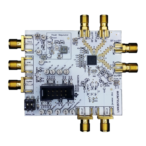
The LMX2572LPEVM is designed to evaluate the performance of LMX2572LP. This board consists of a
LMX2572LP device.
The LMX2572LP is a low-power, high-performance wideband synthesizer that can generate any frequency
from 12.5 MHz to 2 GHz without using an internal VCO doubler. The PLL delivers excellent performance
while consuming just 70 mA from a single 3.3-V supply.
1
..........................................................................................................................
2
3
...................................................................................................................
4
5
6
7
1
2
3
4
....................................................................................................................
5
6
7
SNAU235 - May 2018
Submit Documentation Feedback
LMX2572LPEVM Evaluation Instructions
......................................................................................
.......................................................................................................
.........................................................................................
.............................................................................................................
....................................................................................................
................................................................................
....................................................................................................
..................................................................................................
..................................................................................................
.................................................................................................................
.........................................................................................................
................................................................................................................
..................................................................................................
Copyright © 2018, Texas Instruments Incorporated
Contents
List of Figures
LMX2572LPEVM Evaluation Instructions
User's Guide
SNAU235 - May 2018
3
3
6
13
15
18
19
20
21
3
5
5
5
6
7
7
1
Advertisement
Table of Contents

Related Manuals for Texas Instruments LMX2572LPEVM


Summary of Contents for Texas Instruments LMX2572LPEVM
-
Page 1: Table Of Contents
User's Guide SNAU235 – May 2018 LMX2572LPEVM Evaluation Instructions The LMX2572LPEVM is designed to evaluate the performance of LMX2572LP. This board consists of a LMX2572LP device. The LMX2572LP is a low-power, high-performance wideband synthesizer that can generate any frequency from 12.5 MHz to 2 GHz without using an internal VCO doubler. The PLL delivers excellent performance while consuming just 70 mA from a single 3.3-V supply. - Page 2 Reference PRO Output Frequency Selection ................Reference PRO Output Format Selection ..................Output Termination Configuration Trademarks All trademarks are the property of their respective owners. LMX2572LPEVM Evaluation Instructions SNAU235 – May 2018 Submit Documentation Feedback Copyright © 2018, Texas Instruments Incorporated...
-
Page 3: Lmx2572Lpevm Evaluation Module
A PC running Windows 7 or more recent version • An oscilloscope (optional) • A high quality signal generator (optional) • Texas Instruments Clocks and Synthesizers TICS Pro software • Texas Instruments PLLatinum Simulator Tool (optional) Resources Related evaluation and development resources are as follows: •... - Page 4 Programming Connect the ribbon cable from the Reference PRO to the LMX2572LPEVM. Connect the USB cable from a PC to USB port in the Reference PRO. This provides power supply to the Reference PRO board and communication with the TICS Pro. A firmware update may be required. See Appendix B for more details.
-
Page 5: Select Device In Tics Pro
PLL lock status through the LED D1. By default, both switches are in the Make position. To read back register in TICS Pro, set Switch 2 to the Break position. Figure 4. MUXout_SW Switch SNAU235 – May 2018 LMX2572LPEVM Evaluation Instructions Submit Documentation Feedback Copyright © 2018, Texas Instruments Incorporated... -
Page 6: Typical Measurement
Section 2 to set up the evaluation. 2. Click "Write All Registers" to write all the registers to LMX2572LP. The default output is 1.5 GHz. LMX2572LPEVM Evaluation Instructions SNAU235 – May 2018 Submit Documentation Feedback Copyright © 2018, Texas Instruments Incorporated... -
Page 7: Default Output
Phase shift = 360° × (800 / 1000) × (1 / 32) = 9° The user can write 800 to MASH_SEED 40 times to get the 360° phase shift. Figure 7. Phase Adjustment Setting SNAU235 – May 2018 LMX2572LPEVM Evaluation Instructions Submit Documentation Feedback Copyright © 2018, Texas Instruments Incorporated... -
Page 8: Phase Adjustment
VCO calibration. RAMP_MANUAL = 0 means Automatic Ramping mode. Set RAMP_EN = 1 to start ramping. Set RAMP_EN = 0 to turn off ramping. LMX2572LPEVM Evaluation Instructions SNAU235 – May 2018 Submit Documentation Feedback Copyright © 2018, Texas Instruments Incorporated... -
Page 9: Calibration-Free Automatic Ramp Setting
Ramp up / down time 1000 µs RAMP_LIMIT_HIGH 5060 MHz RAMP_LIMIT_LOW 4540 MHz 100 MHz OSCin CAL_CLK_DIV RAMP_THRESH 40 MHz Pause time for VCO calibration 500 µs SNAU235 – May 2018 LMX2572LPEVM Evaluation Instructions Submit Documentation Feedback Copyright © 2018, Texas Instruments Incorporated... -
Page 10: Automatic Ramp Setting
Table 5. FSK SPI FAST Mode Example PARAMETER EXAMPLE VALUE Phase detector frequency 100 MHz CHDIV PLL_DEN 8000000 FSK_DEV_SCALE Frequency deviation ±648 Hz; ±1944 Hz LMX2572LPEVM Evaluation Instructions SNAU235 – May 2018 Submit Documentation Feedback Copyright © 2018, Texas Instruments Incorporated... -
Page 11: Fsk Spi Fast Mode Setting
Write the correct values to the FSK_SPI_FAST_DEV register field. The output of LMX2572LP is a discrete 4-level FSK modulation signal. Figure 13. FSK SPI FAST Mode Setting Figure 14. FSK SPI FAST Mode SNAU235 – May 2018 LMX2572LPEVM Evaluation Instructions Submit Documentation Feedback Copyright © 2018, Texas Instruments Incorporated... -
Page 12: Readback Setting
3. Click on the Register Name that you want to read back. 4. Click the Read Register button to read back the register value. Figure 16. Register Readback LMX2572LPEVM Evaluation Instructions SNAU235 – May 2018 Submit Documentation Feedback Copyright © 2018, Texas Instruments Incorporated... -
Page 13: Schematic
Schematic www.ti.com Schematic Figure 17. LMX2572LPEVM Schematic (Page 1) SNAU235 – May 2018 LMX2572LPEVM Evaluation Instructions Submit Documentation Feedback Copyright © 2018, Texas Instruments Incorporated... -
Page 14: Lmx2572Lpevm Schematic
Schematic www.ti.com Figure 18. LMX2572LPEVM Schematic (Page 2) LMX2572LPEVM Evaluation Instructions SNAU235 – May 2018 Submit Documentation Feedback Copyright © 2018, Texas Instruments Incorporated... -
Page 15: Pcb Layout And Layer Stack-Up
GND layer FR4 (Er = 4.6) Power layer FR4 (Er = 4.6) Bottom layer Figure 19. PCB Layer Stack-Up PCB Layout Figure 20. Top Layer SNAU235 – May 2018 LMX2572LPEVM Evaluation Instructions Submit Documentation Feedback Copyright © 2018, Texas Instruments Incorporated... -
Page 16: Gnd Layer
PCB Layout and Layer Stack-Up www.ti.com Figure 21. GND Layer Figure 22. Power Layer LMX2572LPEVM Evaluation Instructions SNAU235 – May 2018 Submit Documentation Feedback Copyright © 2018, Texas Instruments Incorporated... -
Page 17: Bottom Layer
PCB Layout and Layer Stack-Up www.ti.com Figure 23. Bottom Layer SNAU235 – May 2018 LMX2572LPEVM Evaluation Instructions Submit Documentation Feedback Copyright © 2018, Texas Instruments Incorporated... -
Page 18: Bill Of Materials
JACK, SMA, 50 Ω, Gold, Edge Mount 142-0771-831 Johnson High Performance, Wideband PLLatinum LMX2572LPRHAR Texas Instruments RF Synthesizer uWire Header (shrouded), 100 mil, 5x2, Gold 52601-S10-8LF plated, SMD LMX2572LPEVM Evaluation Instructions SNAU235 – May 2018 Submit Documentation Feedback Copyright © 2018, Texas Instruments Incorporated... -
Page 19: Troubleshooting Guide
• Register readback requires the correct hardware and software setup. See Section 3.2.5 for details. • The POR current of the LMX2572LPEVM is approximately 30 mA. • The power-down current of the LMX2572LPEVM is approximately 2.5 mA. Start Congratulation! Device locked Verify hardware setup: Validate power supply is connected, turned on, and current limit is appropriate for the device. -
Page 20: Appendix A Using Different Reference Clock
Appendix A SNAU235 – May 2018 Using Different Reference Clock These are the different options to provide a reference clock to LMX2572LPEVM. By default, the EVM is configured for an external single-ended clock. Table 7. Reference Clock Input Configuration INPUT... -
Page 21: Appendix B Reference Pro
The Reference PRO board is used to program the LMX2572LPEVM and provide a clean reference clock to LMX2572LPEVM at the same time. The board has several control pins dedicated for control of output format, output frequency, and output enable control. These control pins are configurable through the jumpers by strapping the center pin to Vdd position or GND position. -
Page 22: Output Termination Schematic
100-Ω differential termination (R31) is provided onboard. Removing this termination is possible if the differential termination is available on the receiver. Figure 25. Output Termination Schematic Reference PRO SNAU235 – May 2018 Submit Documentation Feedback Copyright © 2018, Texas Instruments Incorporated... -
Page 23: Default Output Phase Nosie
Follow the pop-up instructions to complete the update. This update is necessary to ensure that the USB connection between the PC and the Reference PRO board is properly set up, otherwise the programming to LMX2572LPEVM will not be successful. 1. When you see this message, click the "OK" button. -
Page 24: Firmware Loader
2. Next, follow the on-screen procedure. Figure 29. Firmware Loader 3. The BSL button is located next to the USB connector. Figure 30. BSL Button Reference PRO SNAU235 – May 2018 Submit Documentation Feedback Copyright © 2018, Texas Instruments Incorporated... -
Page 25: Update Firmware
5. Click the "Upgrade Firmware" button to start the upgrade and click the "Close" button after the upgrade is complete. Figure 32. Firmware Update Complete SNAU235 – May 2018 Reference PRO Submit Documentation Feedback Copyright © 2018, Texas Instruments Incorporated... -
Page 26: Usb Communications
6. Check the USB connection in TICS Pro by clicking "USB communications" → "Interface". Make sure that the "USB Connected" button is green. Figure 33. USB Communications Reference PRO SNAU235 – May 2018 Submit Documentation Feedback Copyright © 2018, Texas Instruments Incorporated... - Page 27 STANDARD TERMS FOR EVALUATION MODULES Delivery: TI delivers TI evaluation boards, kits, or modules, including any accompanying demonstration software, components, and/or documentation which may be provided together or separately (collectively, an “EVM” or “EVMs”) to the User (“User”) in accordance with the terms set forth herein.
- Page 28 FCC Interference Statement for Class B EVM devices NOTE: This equipment has been tested and found to comply with the limits for a Class B digital device, pursuant to part 15 of the FCC Rules. These limits are designed to provide reasonable protection against harmful interference in a residential installation.
- Page 29 【無線電波を送信する製品の開発キットをお使いになる際の注意事項】 開発キットの中には技術基準適合証明を受けて いないものがあります。 技術適合証明を受けていないもののご使用に際しては、電波法遵守のため、以下のいずれかの 措置を取っていただく必要がありますのでご注意ください。 1. 電波法施行規則第6条第1項第1号に基づく平成18年3月28日総務省告示第173号で定められた電波暗室等の試験設備でご使用 いただく。 2. 実験局の免許を取得後ご使用いただく。 3. 技術基準適合証明を取得後ご使用いただく。 なお、本製品は、上記の「ご使用にあたっての注意」を譲渡先、移転先に通知しない限り、譲渡、移転できないものとします。 上記を遵守頂けない場合は、電波法の罰則が適用される可能性があることをご留意ください。 日本テキサス・イ ンスツルメンツ株式会社 東京都新宿区西新宿6丁目24番1号 西新宿三井ビル 3.3.3 Notice for EVMs for Power Line Communication: Please see http://www.tij.co.jp/lsds/ti_ja/general/eStore/notice_02.page 電力線搬送波通信についての開発キットをお使いになる際の注意事項については、次のところをご覧ください。http:/ /www.tij.co.jp/lsds/ti_ja/general/eStore/notice_02.page 3.4 European Union 3.4.1 For EVMs subject to EU Directive 2014/30/EU (Electromagnetic Compatibility Directive): This is a class A product intended for use in environments other than domestic environments that are connected to a low-voltage power-supply network that supplies buildings used for domestic purposes.
- Page 30 Notwithstanding the foregoing, any judgment may be enforced in any United States or foreign court, and TI may seek injunctive relief in any United States or foreign court. Mailing Address: Texas Instruments, Post Office Box 655303, Dallas, Texas 75265 Copyright © 2018, Texas Instruments Incorporated...
- Page 31 IMPORTANT NOTICE FOR TI DESIGN INFORMATION AND RESOURCES Texas Instruments Incorporated (‘TI”) technical, application or other design advice, services or information, including, but not limited to, reference designs and materials relating to evaluation modules, (collectively, “TI Resources”) are intended to assist designers who are developing applications that incorporate TI products;...
Need help?
Do you have a question about the LMX2572LPEVM and is the answer not in the manual?
Questions and answers