Table of Contents
Advertisement
Quick Links
Advertisement
Table of Contents

Related Manuals for Fuji Electric FRENIC-VG Series


Summary of Contents for Fuji Electric FRENIC-VG Series
- Page 1 User's Manual Option Edition 24A7-E-0045...
- Page 3 High Performance, Vector Control Inverter User's Manual (Option Edition)
- Page 4 Copyright © 2013 Fuji Electric Co., Ltd. All rights reserved. No part of this publication may be reproduced or copied without prior written permission from Fuji Electric Co., Ltd. All products and company names mentioned in this manual are trademarks or registered trademarks of their respective holders.
- Page 5 2) Outline, features, specifications, replacement data, (this manual) etc. of the FRENIC-VG Unit type Functions of various option cards, RS-485 interface, etc. available for the FRENIC-VG series Option Edition 24A7- -0045* * For the optional functional safety card (Old No. MHT286)
- Page 6 How this manual is organized This manual contains Chapters 5 and 6. Chapter 5 USING STANDARD RS-485 This chapter describes the use of standard RS-485 communications ports and provides an overview of the FRENIC-VG Loader. Chapter 6 CONTROL OPTIONS This chapter describes the FRENIC-VG's control options. For other information, refer to the FRENIC-VG User's Manuals (Unit Type / Function Codes Edition and Stack Type Edition).
-
Page 7: Table Of Contents
CONTENTS Chapter 5 USING STANDARD RS-485 Standard RS-485 Communications Ports....................5-1 5.1.1 RS-485 common specifications......................5-2 5.1.2 Terminal specifications for RS-485 communications ................ 5-3 5.1.3 Connection method ..........................5-4 5.1.4 Communications support devices ...................... 5-6 5.1.4.1 Converters ..........................5-6 5.1.4.2 Cables............................ - Page 8 5.3.3.4 Calculating frame length ......................5-43 5.3.4 Communication examples........................ 5-44 5.3.4.1 Reading ............................ 5-44 FRENIC-VG Loader..........................5-45 5.4.1 Specifications........................... 5-45 5.4.2 Connection ............................5-46 5.4.2.1 USB connection ........................5-46 5.4.2.2 RS-485 connection ........................5-47 5.4.2.3 Communication via MICREX-SX ................... 5-47 5.4.3 Function overview ...........................
- Page 9 6.3.2.2 Specifications ........................... 6-45 6.3.2.3 Using the card in combination with a Fuji motor..............6-46 6.3.3 External dimension diagram ......................6-47 6.3.4 Basic connection diagram ........................ 6-48 6.3.4.1 Line driver type........................6-49 6.3.4.2 Open collector output type ....................... 6-50 6.3.4.3 Connection Diagram for Fuji servos ..................
- Page 10 6.5.11.2 Application program examples ....................6-116 6.5.12 Multiple option application examples .................... 6-118 6.5.12.1 Installed with T-Link interface card ..................6-118 6.5.12.2 Installed with high-speed serial communication-capable terminal block....... 6-119 High-Speed Serial Communication-Capable Terminal Block OPC-VG1-TBSI........6-120 6.6.1 Product overview ........................... 6-120 6.6.1.1 Multiplex system........................
- Page 11 6.7.11.2 Remote register signal in 4 X mode (o32=3) ................. 6-180 6.7.12 8 X mode with 1 station occupied (o32=4) ..................6-182 6.7.12.1 Remote I/O signal in 8 X mode (o32=4)................6-182 6.7.12.2 Remote register signal in 8 X mode (o32=4) ................. 6-182 6.7.13 Link function..........................
- Page 12 6.11.6 Check functions ..........................6-225 6.11.6.1 Option installation check......................6-225 6.11.6.2 I/O check ..........................6-225 6.12 DIO Expansion Card OPC-VG1-DIO ....................6-226 6.12.1 Product overview ........................... 6-226 6.12.2 Models and specifications ......................6-227 6.12.2.1 Models............................ 6-227 6.12.2.2 Specifications ......................... 6-228 6.12.3 Dimensions ............................
- Page 13 6.15.10.3 Action when synchronization is lost ( )................6-266 6.15.11 Support tool interface........................6-267 6.15.11.1 Configuration definition method.................... 6-267 6.15.11.2 Compatible versions of the SPH3000MM and support tool........... 6-267...
- Page 14 Safety precautions Read this manual thoroughly before proceeding with installation, connections (wiring), operation, or maintenance and inspection. Ensure you have sound knowledge of the device and familiarize yourself with all safety information and precautions before proceeding to operate the inverter. Safety precautions are classified into the following two categories in this manual.
- Page 15 Wiring • If no zero-phase current (earth leakage current) detective device such as a ground-fault relay is installed in the upstream power supply line in order to avoid the entire power supply system's shutdown undesirable to factory operation, install a residual-current-operated protective device (RCD)/earth leakage circuit breaker (ELCB) individually to inverters to break the individual inverter power supply lines only.
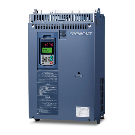
- Page 16 Operation • Be sure to mount the front cover before turning the power ON. Do not remove the cover when the inverter power is ON. Otherwise, an electric shock could occur. • Do not operate switches with wet hands. Doing so could cause electric shock. •...
- Page 17 Maintenance and inspection, and parts replacement • Before proceeding to the maintenance/inspection jobs, turn OFF the power and wait at least five minutes for inverters with a capacity of 22 kW or below, or at least ten minutes for inverters with a capacity of 30 kW or above.
- Page 18 Icons The following icons are used throughout this manual. This icon indicates information which, if not heeded, can result in the inverter not operating to full efficiency, as well as information concerning incorrect operations and settings which can result in accidents. This icon indicates information that can prove handy when performing certain settings or operations.
-
Page 19: Chapter 5 Using Standard
FRENIC- Chapter 5 USING STANDARD RS-485 This chapter describes the use of standard RS-485 communications ports and provides an overview of FRENIC-VG Loader. Contents Standard RS-485 Communications Ports .................... 5-1 5.1.1 RS-485 common specifications....................5-2 5.1.2 Terminal specifications for RS-485 communications..............5-3 5.1.3 Connection method ........................ - Page 20 5.2.6.1 Data field..........................5-28 5.2.6.2 Sum-check field ........................5-29 5.2.7 Communication examples ......................5-29 5.2.7.1 Standard frame ......................... 5-29 5.2.7.2 Option frame ..........................5-30 5.2.7.3 ASCII code table ........................5-31 5.2.7.4 Program example ........................5-32 Modbus RTU............................. 5-33 5.3.1 Message format ......................... 5-33 5.3.2 Transmission frame ........................
-
Page 21: Standard Rs-485 Communications Ports
5.1 Standard RS-485 Communications Ports Standard RS-485 Communications Ports The FRENIC-VG has standard 1-channel RS-485 communications ports. The RS-485 communications ports are assigned in the control terminal block, enabling easy multi-drop connection. RS-485 enables the following communications functions. (1) Communication through Modbus RTU / Fuji general-purpose inverter protocol The FRENIC-VG can be connected to a host (master) device such as a PC, PLC, or display/operation device. -
Page 22: Common Specifications
5.1.1 RS-485 common specifications Items Specifications Protocol SX protocol Modbus RTU Fuji general-purpose inverter (For FRENIC-VG Loader) protocol Compliance Loader dedicated protocol (Not Modicon Modbus RTU-compliant Fuji general-purpose inverter disclosed) protocol Protocol Function code H40 = "1" Function code H40 = "2" Function code H40 = "0"... -
Page 23: Terminal Specifications For Rs-485 Communications
5.1 Standard RS-485 Communications Ports 5.1.2 Terminal specifications for RS-485 communications The FRENIC-VG has terminals for RS-485 communications on the control circuit terminal block. Signal name Function Remarks Built-in terminating resistor: 112Ω DX - RS-485 data (-) Open/close by SW4* DX + RS-485 data (+) *For details about SW4, refer to Chapter 3, Section 3.3.3.9 "Setting up the slide switches."... -
Page 24: Connection Method
(1) Multi-drop connection using the RS-485 communications port Host equipment Host equipment USB or RS-232C RS-485 (4-wire) OUT- OUT+ Terminating resistor Shield RS-485 converter (112 Ω) FRENIC-VG series Inverter 1 RS-232C RS-485 converter Station No. 01 DX+ commercially-available DX- (2-wire) (2-wire) Using the built-in FRENIC-VG series... - Page 25 5.1 Standard RS-485 Communications Ports (2) Connection with a 4-wire type host device Although the cables used with the converter are 2-wire types, some host devices use 4-wire type cables. When connecting to such a host device, it is necessary to change to a 2-wire type connection by connecting the driver output on the host device side with the receiver input using transition wiring.
-
Page 26: Communications Support Devices
5.1.4 Communications support devices This section describes the devices required for connecting the inverter to a PC having no RS-485 interface or for connecting two or more inverters in multi-drop network. 5.1.4.1 Converters Usually PCs are not equipped with an RS-485 communications port. Therefore, it is necessary to use an RS-232C–RS-485 converter or a USB–RS-485 converter. -
Page 27: Cables
5.1 Standard RS-485 Communications Ports 5.1.4.2 Cables To ensure the reliability of connection, use twisted pair shield cables for long distance transmission AWG 16 to 26. Recommended cable manufacturer: FURUKAWA Electric Co., LTD AWM2789 Cable for long distance connection Type (Product code): DC23225-2PB 5.1.5 Link functions Communications functions such as RS-485 are called link functions. -
Page 28: Link Edit Permission Selection
Link commands In link command allowed mode, you can use function code H30 (link function) to link (COM) the command data and the run operation command, and switch between Remote and Local. At this time, REM (Remote: run operation via terminal block) or LOC (Local: run operation via keypad) is displayed. -
Page 29: Referencing And Changing Data
5.1 Standard RS-485 Communications Ports 5.1.6 Referencing and changing data If the system does not have field options, writing to the S range (run operation command, command data) via RS-485 constantly enabled. Additionally, refer to the communications address, 485 No. in Chapter 4, Section 4.2 "Function Code Tables"... -
Page 30: Negative Response And Error Response
(4) Data protection Writing via RS-485 is not restricted by function code F00 [Protect Data]. This code only protects data in the case of keypad operation. Writing via RS-485 is restricted by function code H29 [Protect Link Function] and the [WE-LK] X function (Refer to section 5.1.5.2). -
Page 31: Rs-485 Function Codes
5.1 Standard RS-485 Communications Ports 5.1.7 RS-485 function codes Function code Data setting Remarks Specify station number when connecting to inverter 0 to 255 No response returned when Broadcast is RS-485 setting selected 1 to 247: RTU (station address) 0: Broadcast when RTU selected 1 to 31: Fuji general-purpose 99: Broadcast when Fuji general-purpose selected... -
Page 32: Disconnection Detection Time (H38)
5.1.7.2 Disconnection detection time (H38) If communication from the master (PLC, PC) during RS-485 linked operation (S06: operation command FWD, REV) exceeds the specified time, an RS-485 communication error ( ) is immediately generated. When performing non-fixed cycle communications, disable this function (setting: "0"). -
Page 33: Host Side Procedures
5.1 Standard RS-485 Communications Ports 5.1.8 Host side procedures Please follow the flow chart for each frame transmission procedure. For both reading and writing, always confirm the response before sending the next frame. If there is no response from the inverter after a certain time, execute a timeout and retry. (If you attempt to start a retry before a timeout, the request frame will not be received properly.) Retry When executing a retry, either use a standard frame to resend the data that was sent before no... -
Page 34: Write Procedure
5.1.8.2 Write procedure Start Request frame sent Transmission error detected Response frame received? Normal (ACK) response? Change to correct format and resend. Format error? Change to correct command and Command error? resend. Operation via this communication is Link priority? disabled during link option connection. Change to correct function code and Function code error? resend. -
Page 35: Ras
5.1 Standard RS-485 Communications Ports 5.1.9 5.1.9.1 Communication errors Depending on the usage environment, noise generated by the inverter may prevent normal communications or cause equipment such as instrumentation on the master and converters to malfunction. The following measures may be effective in such cases. Please also refer to the appendix on electrical noise. - Page 36 Change earth: Do not use a common earth for instrumentation and the inverter. Noise may propagate from the earth wire. Additionally, use thick earth wires. Isolated power Noise may propagate from the power supply of instrumentation. supply: To isolate the wiring from the power supply of the inverter, it is recommended to change the power wiring, or use an isolated transformer (TRAFY) for the power supply or a noise-suppressing transformer.
- Page 37 5.1 Standard RS-485 Communications Ports (2) Measures on side generating noise Carrier frequency: It is possible to lower the noise level by lowering the setting of function code F26 [Motor operation noise (carrier frequency)]. However, be aware that lowering the carrier frequency can result in higher levels of noise from other sources.
-
Page 38: Communication Error Measures
5.1.10 Communication error measures When executing run commands or applying command data via RS-485, it is possible to continue running the inverter without tripping the alarm, even if there is a transmission error, by implementing the following measures. The following examples show communication alarms (keypad displays er5) generated when operating the inverter from the master side. -
Page 39: Fuji General-Purpose Communications
5.2 Fuji General-purpose Communications Fuji General-purpose Communications 5.2.1 Message format Polling/selecting is used for the response message format. The inverter is in a constant standby state, waiting for either selecting (write request) or polling (read request) from the host (PC, PLC). The inverter receives a request frame with the same station address from the host while in the standby state. -
Page 40: Standard Frame
5.2.3 Standard frame Request frame [Host Inverter] Station No. Command Type Function code No. Data (byte) BCC target Values Byte Field Description ASCII format Hexadecimal format Transmission begins Station No. '0' - '3', '9' - 33 , 39 Inverter station address (Decimal: tens place) '0' - '9' - 39 Inverter station address (Decimal: ones place) - Page 41 5.2 Fuji General-purpose Communications ACK response frame [Inverter Host] Station No. Command Type Function code No. Data (byte) BCC target Values Byte Field Description ASCII format Hexadecimal format Transmission begins Station No. '0' - '3', '9' - 33 , 39 Inverter station address (Decimal: tens place) '0' - '9' - 39...
- Page 42 NAK response frame [Inverter Host] Station No. Command Type Function code No. Data (byte) BCC target Values Byte Field Description ASCII format Hexadecimal format Transmission begins Station No. '0' - '3', '9' - 33 , 39 Inverter station address (Decimal: tens place) '0' - '9' - 39 Inverter station address (Decimal: ones place)
-
Page 43: Option Frame
5.2 Fuji General-purpose Communications 5.2.4 Option frame Selecting request frame [Host Inverter] Station No. Command Data (byte) BCC target Values Byte Field Description ASCII format Hexadecimal format Transmission begins Station No. '0' - '3', '9' - 33 , 39 Inverter station address (Decimal: tens place) '0' - '9' - 39 Inverter station address (Decimal: ones place) - Page 44 Selecting response frame [Inverter Host] ACK/NAK Station No. Command (byte) BCC target Values Byte Field Description ASCII format Hexadecimal format Transmission begins Station No. '0' - '3', '9' - 33 , 39 Inverter station address (Decimal: tens place) '0' - '9' - 39 Inverter station address (Decimal: ones place) ACK/NAK...
- Page 45 5.2 Fuji General-purpose Communications Polling request frame [Host Inverter] Station No. Command (byte) BCC target Values Byte Field Description ASCII format Hexadecimal format Transmission begins Station No. '0' - '3', '9' - 33 , 39 Inverter station address (Decimal: tens place) '0' - '9' - 39 Inverter station address (Decimal: ones place)
- Page 46 Polling response frame [Inverter Host] ACK/NA Data Station No. Command (byte) BCC target Values Byte Field Description ASCII format Hexadecimal format Transmission begins Station No. '0' - '3', '9' - 33 , 39 Inverter station address (Decimal: tens place) '0' - '9' - 39 Inverter station address (Decimal: ones place) ACK/NAK...
-
Page 47: Negative Response Frame
5.2 Fuji General-purpose Communications 5.2.5 Negative response frame In cases where the length of the response frame varies according to the command type, if the command type character is determined properly, the frame length designated for that command is generally used for the response. Negative response Frame/command type Cause of error... -
Page 48: Field Descriptions
5.2.6 Field descriptions 5.2.6.1 Data field Standard frame SP additional data character character character character Option frame character character character character Except for some special cases, the length of all data is 16 bits. In the data field of a transmission frame, the data format is hexadecimal (0000H-FFFFH), and each digit is expressed as an ASCII code. -
Page 49: Sum-Check Field
5.2 Fuji General-purpose Communications 5.2.6.2 Sum-check field This field contains data used to check for errors in the transmission frame when sending data. The data is calculated by adding all fields except for the S0H and sum-check fields in 1 byte increments. The lowest 1 byte of data is expressed as an ASCII code. -
Page 50: Option Frame
5.2.7.2 Option frame (1) Selecting run command (write) Request frame (Host Inverter) ........ FWD command ACK response frame (Inverter Host) NAK response frame (Inverter Host) ..... Cause of error confirmed to be "M26: Send error process code" (2) Polling torque command value (read) Request frame (Host Inverter) ACK response frame (Inverter... -
Page 51: Ascii Code Table
Shaded codes are used with this communication. Example: For "0," ASCII code is "30 ." For "1," ASCII code is "31 ." Note 1: Codes after "80 " are unique codes specified by Fuji Electric. For settings, use binary. 5-31... -
Page 52: Program Example
5.2.7.4 Program example This program is written in Microsoft QuickBASIC (MS-DOS QBasic), and runs in accordance with Fuji general-purpose inverter protocol. 'FGI-Bus Sample Program(MS-DOS QBasic) OPEN "COM1:38400,E,8,1" FOR RANDOM AS #1 'ComPort:BaudRate,Parity,DataBits,StopBits soh$ = CHR$(1) 'FunctionCode H34, H36, H35, etx$ = CHR$(3) enq$ = CHR$(5) ack$ = CHR$(6) nak$ = CHR$(&H15) -
Page 53: Modbus Rtu
5.3 Modbus RTU Modbus RTU This communications protocol was created overseas. Where possible, English text is used alongside the Japanese. 5.3.1 Message format The normal format for sending RTU messages is as follows. 1. Query Host Query message Response Inverter 2. -
Page 54: Transmission Frame
5.3.2 Transmission frame The transmission frame is as follows. 1 byte 1 byte max. 203 bytes 2 bytes Station address FC (function code) Information Error check (1) Station address (station number) Station addresses 0 to 247 are selectable with a 1 byte length. Selecting a "0"... -
Page 55: Reading Function Codes
5.3 Modbus RTU 5.3.2.1 Reading function codes Query 1 byte 1 byte 2 bytes 2 bytes 2 bytes Function code Read data size (max. 99) Error check Station No. Normal response 1 byte 1 byte 1 byte 2 to 198 bytes 2 bytes Byte count Read data size (max. -
Page 56: Writing Single Function Codes
5.3.2.2 Writing single function codes Query 1 byte 1 byte 2 bytes 2 bytes 2 bytes Function code Write data Error check Station No. Normal response 1 byte 1 byte 2 bytes 2 bytes 2 bytes Function code Write data Error check Station No. -
Page 57: Writing Multiple Function Codes
5.3 Modbus RTU 5.3.2.3 Writing multiple function codes Query 1 byte 1 byte 2 bytes 2 bytes 1 byte 2 to 32 bytes 2 bytes Station No. Function code Write data size Byte count Write data Error check Hi, Lo, Hi, Lo,… Normal response 1 byte 1 byte... -
Page 58: Maintenance Code
5.3.2.4 Maintenance code This function is used to check communication line connections (hardware). Query 1 byte 1 byte 2 bytes 2 bytes 2 bytes Diagnosis code 00 00 Data Error check Station No. Normal response 1 byte 1 byte 2 bytes 2 bytes 2 bytes Diagnosis code 00 00... -
Page 59: Error Response
5.3 Modbus RTU 5.3.2.5 Error response If an incorrect query is received, the query is not processed and an error response is returned. Error response 1 byte 1 byte 1 byte 2 bytes Station No. Exception function Sub code Error check Interpreting "Error response"... -
Page 60: Error Checking
5.3.3 Error checking 5.3.3.1 CRC-16 When sending data, CRC data is used to check for errors in the transmission frame. CRC is the most effective system for error checking. At the sending side, the CRC value is calculated and added to the last level of the frame. Then, at the receiving side, the CRC value is calculated again in the same way based on the received data. -
Page 61: Crc-16 Algorithm
5.3 Modbus RTU 5.3.3.2 CRC-16 algorithm The following diagram shows the CRC-16 calculation algorithm. Please also refer to the calculation example in Section 5.3.3.3. START Default 初期設定 Remainder R “FFFF” 余り R ← "FFFF" Generating polynomial P “A001” 生成多項式 P ← "A001" Data length counter n データ長カウンタ... -
Page 62: Crc-16 Calculation Example
5.3.3.3 CRC-16 calculation example The following is an example of read data that is sent: Station number: 1, FC = 03, function code P49 (P = code 03, 49 = 31 Hex), read data size: 20 items, G.P (generating polynomial): 1010 0000 0000 0001. Address Function code Read data size... -
Page 63: Calculating Frame Length
5.3 Modbus RTU PROCESS Flag Shift >> 1 CRC = No.35 X or G.P Shift >> 1 CRC = No.37 X or G.P Shift >> 1 CRC = No.37 X or G.P Shift >> 3 CRC = No.41 X or G.P Shift >>... -
Page 64: Communication Examples
5.3.4 Communication examples This section illustrates representative communication examples. (In all cases, the station number is 5.3.4.1 Reading (1) M06: Read speed detection value. Query (Host Inverter) Normal response (Inverter Host) Speed detection value: 2710 10000d Max. speed 10000d x = 750 (r/min) 20000 (Max. -
Page 65: Frenic-Vg Loader
5.4 FRENIC-VG Loader FRENIC-VG Loader Inverter support software FRENIC-VG Loader runs on a computer to provide the following. • Configuring and managing function codes: Reading/writing function code data from/to the inverter • Monitoring the running status of the FRENIC-VG: Operation monitor (I/O monitor and system monitor) Trace functions (Real-time trace and historical trace) •... -
Page 66: Connection
Item Specifications Remarks OS *2 Microsoft Windows XP (SP3 or later) Microsoft Windows Vista Microsoft Windows 7 (32-bit, 64-bit) Memory 512 MB or more RAM 2 GB or more recommended Hard disk space Free space of 8.5 MB or more Serial ports USB port The FRENIC5000VG7 requires... -
Page 67: Communication Via Micrex-Sx
5.4 FRENIC-VG Loader 5.4.2.2 RS-485 connection The FRENIC-VG or FRENIC5000VG7 has an RS-485 communications interface as standard, enabling access from FRENIC-VG Loader in RS-485 communication. Connecting the inverter to a computer requires an RS-485 converter. In the maximum configuration, up to 31 inverters can be connected to a single computer running FRENIC-VG Loader. When two or more inverters are connected, it is necessary to register each inverter (station address, etc.) for access from FRENIC-VG Loader. -
Page 68: Function Overview
5.4.3 Function overview This section overviews the functions of FRENIC-VG Loader. For details, refer to the FRENIC-VG Loader Instruction Manual. 5.4.3.1 Configuring function codes FRENIC-VG Loader allows you to edit, set, and check (comparison between data saved in the inverter and that in the connected computer) the function codes of the FRENIC-VG or FRENIC5000VG7. - Page 69 5.4 FRENIC-VG Loader Trace specifications Item Traceback Real-time trace Historical trace Detected current value, Detected current value, angle of current flow angle of current flow 50 μs to 83.36 μs 50 μs to 83.36 μs 100 μs to 166.72 μs 100 μs to 166.72 μs Sampling time 1 ms to 1s...
-
Page 70: Operation Monitor
5.4.3.3 Operation monitor FRENIC-VG Loader can monitor the following and save the monitored data in CSV format. 1 I/O monitor: This monitors the ON/OFF states of the input and output terminals of the inverter. 2 System monitor: This shows the inverter ROM version, inverter type, current setup information, and maintenance information of the inverter. - Page 71 FRENIC- Chapter 6 CONTROL OPTIONS This chapter describes the FRENIC-VG's control options. Contents Common Specifications ........................6-1 6.1.1 Specifications table ........................6-1 6.1.2 Inspecting options after delivery ....................6-4 6.1.2.1 Inspecting options ........................6-4 6.1.2.2 Operating environment....................... 6-5 6.1.3 Storing options ..........................6-6 6.1.3.1 Temporary storage........................
- Page 72 6.2.6 Check functions......................... 6-42 6.2.6.1 Optional equipment check......................6-42 6.2.6.2 I/O check ..........................6-42 6.2.7 Protective functionality ......................6-42 Synchronous Motor Drive PG Interface Card OPC-VG1-PMPG/PMPGo ........6-43 6.3.1 Product overview........................6-43 6.3.2 Model and specifications......................6-44 6.3.2.1 Model ............................6-44 6.3.2.2 Specifications ...........................
- Page 73 6.5.7.2 Area occupied and data allocation addresses ................6-91 6.5.8 Transmission format........................6-97 6.5.8.1 Data Format (FRENIC-VG ⇒ MICREX-SX) ................. 6-97 6.5.8.2 Data format (MICREX-SX ⇒ FRENIC-VG)................ 6-102 6.5.9 Link function........................... 6-110 6.5.10 Data transmission example...................... 6-110 6.5.11 System configuration definition ....................6-112 6.5.11.1 Programming support tool expert (D300win) ................
- Page 74 6.7.9.1 Remote I/O signal in 1 X mode (o32=1)................6-173 6.7.9.2 Remote register signal in 1 X mode (o32 = 1) ............... 6-175 6.7.9.3 Monitor code/command code (o32 = 1 to 4)................6-176 6.7.10 2 X mode with 1 station occupied (o32=2)................6-179 6.7.10.1 Remote I/O signal in 2 X mode (o32=2)................
- Page 75 6.11.2.1 Model ............................. 6-217 6.11.2.2 Specifications ......................... 6-218 6.11.3 External dimension drawing....................6-220 6.11.4 Basic connection diagram ....................... 6-221 6.11.5 Function codes ........................6-222 6.11.5.1 Data latch function ......................... 6-222 6.11.5.2 Selecting binary or BCD input ....................6-223 6.11.5.3 Controlled variable input......................6-224 6.11.6 Check functions........................
- Page 76 6.15.7.2 Input/output data address assignments ................... 6-260 6.15.8 Format details.......................... 6-261 6.15.8.1 I area (MICREX-SX ← FRENIC-VG) ................6-261 6.15.8.2 Q area (MICREX-SX → FRENIC-VG) ................6-263 6.15.9 Data transmission examples ....................6-264 6.15.10 Synchronization of E-SX bus tact cycle and inverter control cycle ........6-266 6.15.10.1 Conditions required for tact synchronization..............
-
Page 77: Common Specifications
6.1 Common Specifications Common Specifications 6.1.1 Specifications table Table 6.1.1 Switch-accessible Category Name Model Specifications functions Section F/V converter OPC-VG1-FV F/V converter (*1) Analog cards Synchro interface OPC-VG1-SN Dancer control synchro interface circuit 6.10 Aio expansion card OPC-VG1-AIO 2 [Ai] + 2 [Ao] expansion card 6.13 16-bit Di binary or BCD 4-digit + sign OPC-VG1-DIA... - Page 78 For options whose manuals are separately issued as shown in the above table, refer to the documents listed below. Model Name Material No. Remarks OPC-VG1-SIU UPAC communication high-speed serial card 24A7- -0044* OPC-VG1-UPAC User Programmable Application Card (UPAC) OPC-VG1-SAFE Functional safety card INR-SI47-1541*- WPS-VG1-STR FRENIC-VG Loader (free version)
- Page 79 6.1 Common Specifications The following table indicates which control options can be used in combination (number of options mountable): Table 6.1.2 Port Category Pattern 1 Pattern 2 Pattern 3 Digital 8-bit, analog card Digital 8-bit Filed bus interface card Digital 16-bit Safety cards Control circuit terminals Constraints when an OPC control option is installed...
-
Page 80: Inspecting Options After Delivery
6.1.2 Inspecting options after delivery 6.1.2.1 Inspecting options • Do not use products with damaged or missing parts. Doing so may result in bodily injury or damage. Once you receive the product you ordered, check the following items: Verify that the product you received is in fact the product you ordered. Check the type/model printed on the option. -
Page 81: Operating Environment
6.1 Common Specifications 6.1.2.2 Operating environment Options are designed for use in the same operating environment as the FRENIC-VG. Table 6.1.5 Operating Environment Item Specifications Installation location Shall be free from corrosive gases, flammable gases, oil mist, dusts, and direct sunlight. (Pollution degree 2 (IEC60664-1)). -
Page 82: Storing Options
6.1.3 Storing options 6.1.3.1 Temporary storage Options should be stored in an environment that satisfies the conditions listed in Table 6.1.6. Table 6.1.6 Storage Environment Item Specifications Ambient -10 to +50°C temperature Avoid use in environments where abrupt changes in temperature Storage temperature -25 to +70°C may cause condensation or freezing. -
Page 83: Installing Internal Options (Opc-Vg1- )
6.1 Common Specifications 6.1.4 Installing internal options (OPC-VG1- 6.1.4.1 Removing the front cover • Inappropriate installation or removal of the product may cause damage to the product. • Shut off the inverter's input power supply and verify that the charge lamp (CHARGE) has gone out before installing or removing options. -
Page 84: Installing A Digital 8-Bit Communications Option Card
6.1.4.2 Installing a digital 8-bit communications option card The following options ("communications option cards") are connected to either A port (CN3) or B port (CN2) on the control printed circuit board. • When not using the communications option card at the same time as a digital Options 16-bit option (OPC-VG1-SX, etc.), follow "Installation method 1"... - Page 85 6.1 Common Specifications Installation method 2 (when using the option at the same time as a digital 16-bit option card) The dimensions of the spacers included with communications option cards and those included with digital 16-bit option cards differ slightly. See the following diagram when determining which spacers to use. Use of the wrong spacers may damage the product.
-
Page 86: Installing A Digital 8-Bit Option Card
6.1.4.3 Installing a digital 8-bit option card The following options ("digital option card") can be connected to either A port (CN3) or B port (CN2) on the control printed circuit board. However, the OPC-VG1-SPGT must be connected to B port (CN2). •... - Page 87 6.1 Common Specifications Installation method 2 (when using the option at the same time as a digital 16-bit option card) The dimensions of the spacers included with digital option cards and those included with digital 16-bit option cards differ slightly. See the following diagram when determining which spacers to use. Use of the wrong spacers may damage the product.
-
Page 88: Installing A Digital 16-Bit Option Card
Power supply Power supply harness harness CN25 CN12 D port D port Digital 16-bit A port Digital 16-bit B port option option CN24 Power Power supply ① ① supply harness ③ ③ harness ② ④ ② ④ ⑤ ⑤ ⑥ ⑥... - Page 89 6.1 Common Specifications Installation procedure 1 (when not using the option together with a digital 16-bit option card) (1) Attach the three included spacers (d) to the three option mounting fixtures (a) through (c) on the control printed circuit board. (2) Install the analog option card so that connector CN1 (on the back of the analog option card) connects to A port (CN3) on the control printed circuit board.
- Page 90 Installation procedure 2 (when using the option together with a digital 16-bit option card) The dimensions of the spacers included with analog option cards and those included with digital 16-bit option cards differ slightly. See the following diagram when determining which spacers to use. Use of the wrong spacers may damage the product.
-
Page 91: Installing A Field Bus Interface Card
6.1 Common Specifications 6.1.4.6 Installing a field bus interface card The following options ("interface card") can be connected to C port (CN6) on the control printed circuit board. Options OPC-VG1-PVP OPC-VG1-DEV Installation procedure (1) Attach one spacer (b) included with the interface card to the option mounting fixture (a) on the control printed circuit board. -
Page 92: Installing A Functional Safety Card
6.1.4.7 Installing a functional safety card The following options can be connected to E port (CN16) on the control printed circuit board. Options OPC-VG1-SAFE Installation procedure (1) Install the functional safety card so that connector CN6 (on the back of the functional safety card) connects to E port (CN16) on the control printed circuit board. -
Page 93: Installing A Control Circuit Terminal Option
6.1 Common Specifications 6.1.4.8 Installing a control circuit terminal option The following options can be connected to F port (CN1) on the control printed circuit board. Options OPC-VG1-TBSI Installation procedure (1) Loosen two screws (a) on the standard control circuit terminal printed circuit board and remove the board from F port (CN1) on the control printed circuit board. -
Page 94: Pg Interface Expansion Card Opc-Vg1-Pg
PG Interface Expansion Card OPC-VG1-PG/PGo 6.2.1 Product overview The PG interface expansion card is used for speed control using a line driver output type of encoders, synchronous operation of two or more motors, and rotational positioning (orientation). Since the FRENIC-VG's built-in PG interface generates 15 V and 12 V complementary (totem pole, push-pull) output, the built-in PG interface function is used when performing speed control with PG feedback using a normal FRENIC-VG standard motor. -
Page 95: Model And Specifications
6.2 PG Interface Expansion Card 6.2.2 Model and specifications 6.2.2.1 Model • There are two models for the PG interface expansion card, reflecting differences in the external equipment output interface: OPC-VG1-PG: Line driver signals OPC-VG1-PGo: Open collector/voltage output Take care not to specify the wrong model when placing an order for cards. The available models of FRENIC-VG's PG options differ according to the external equipment output interface (line driver output, open collector output/voltage output). -
Page 96: Specifications
6.2.2.2 Specifications Failure to set the switches (SW1) on the PG interface expansion card correctly will prevent the • system from operating properly. Read information about the settings below and be sure to set the switches correctly. When performing rotational positioning, set the switches to PG (PD). Use of the card in this •... - Page 97 6.2 PG Interface Expansion Card Input signal format (run reverse signals * omitted) 2 signals with a 90° phase difference Run forward Run reverse Input A pulse Input B pulse Command pulse, command code Run forward Run reverse Input A pulse Input B pulse OPC-VG1-PG t1,t2>4us...
- Page 98 (2) Line speed control specifications: OPC-VG1-PG (LD) This configuration is used when controlling the line speed of a winding device using a PG installed on the line, rather than motor speed control. Figure 6.2.4 Table 6.2.4 Item Line speed control specifications Card type (setting) OPC-VG1-PG (LD)
- Page 99 6.2 PG Interface Expansion Card (3) Pulse train command and pulse train synchronous operation specifications: OPC-VG1-PG (PR) Operation conforms to pulse train command input. Master/slave pulse train synchronous operation is possible. Figure 6.2.5 Table 6.2.5 Item Pulse train command and pulse train synchronous operation specifications Card format (setting) OPC-VG1-PG (PR)
- Page 100 (4) Orientation specifications: OPC-VG1-PG (PD) This configuration enables rotational positioning control using a UPAC. For details, refer to the UPAC User's Manual. Figure 6.2.7 Table 6.2.6 Item Orientation specifications Two cards required Card format (setting) OPC-VG1-PG (PD) UPC-VG1-UPAC H10020 or later, H20020 or later Inverter ROM version The above ROM version should be used.
- Page 101 6.2 PG Interface Expansion Card Table 6.2.7 Item Orientation specifications Orientation package (WPS-VG1-POS) Number of speed change 4 (switchable with contact inputs RT1 and RT2. gear shifts Gradual stop function for stop operation Stop direction selectable such as shortcut Operation selection Function selection, e.g., Speed-up and shortest stopping distance, or stop without speed-up Orientation command...
-
Page 102: External Dimension Diagram
6.2.3 External dimension diagram (Unit: mm) Figure 6.2.9 OPC-VG1-PG Outline Drawing Figure 6.2.10 OPC-VG1-PGo Outline Drawing 6-26... -
Page 103: Basic Connection Diagram
6.2 PG Interface Expansion Card 6.2.4 Basic connection diagram Refer to "6.1.4 Installing Built-in Options (OPC-VG1- )" before performing wiring or connection work. • Performing connection work in an inappropriate manner may result in electric shock, fire, or other damage. Qualified electricians should carry out wiring. -
Page 104: Wiring
6.2.4.2 Wiring Wiring between the PG interface expansion card and a pulse generator, PG, or other device • Use shielded wire for PG interface expansion card wiring. Wiring length is subject to constraints depending on the interface type (see table below). •... -
Page 105: Speed Control
6.2 PG Interface Expansion Card 6.2.4.3 Speed control This connection example illustrates how to drive a motor (a Fuji servomotor, etc.) to which a line driver output type encoder or open collector or complementary type encoder. Since the speed is detected and calculated based on received pulses, the PG interface expansion card must be set to SD. -
Page 106: Line Speed Control
6.2.4.4 Line speed control This connection example illustrates how to perform speed control after installing a line Direction of line Winding operation driver output type encoder on a system's winding line. Since motor speed feedback and line speed feedback can be detected NTC thermistor simultaneously, it is possible to prevent a runaway operation scenario resulting from a... - Page 107 6.2 PG Interface Expansion Card Line driver output MOTOR FRENIC-VG The PG interface expansion card operates by 1500 Main power supply L1/R receiving pulse commands from an external 3-phase power L2/S supply pulse generator or PG. 50/60Hz L3/T NTC thermistor [TH1] Since the FRENIC-VG receiving these [PA]...
-
Page 108: Orientation
6.2.4.6 Orientation This section gives a connection example to perform rotation positioning using an encoder mounted on the machine axis. The option detects pulses including Z-phase, so "PD" should be selected. The Z-phase is for detecting an absolute position of the machine. The stop position and orientation commands can be entered through the T-link, DI card, built-in RS-485, field bus, etc. -
Page 109: Synchronized Operation
6.2 PG Interface Expansion Card 6.2.5 Synchronized operation 6.2.5.1 Synchronized operation system architecture Systems for synchronously operating motors with a FRENIC-VG utilize master/slave connections, cascading connections, or pulse train commands from a PLC or other external transmitter. Master/slave connections • When using a master/slave connection, up to one FRENIC-VG can be connected in parallel to the slave side of the system (8 mA sink current/1 circuit). - Page 110 This connection method is used when Master connecting two or more slave units in a FRENIC-VG master/slave connection. 1500 The description in (1) above applies between the master and the first slave unit, but function code E29 must be set between the first and second slave units.
-
Page 111: Synchronized Operation Method
6.2 PG Interface Expansion Card The direction of rotation for slave motors is determined by [IVS] and the pulse input format. Table 6.2.13 Slave direction of operation B-phase high A-phase input B-phase, 90° advance Forward B-phase high A-phase input B-phase, 90° advance Reverse B-phase low B-phase input... - Page 112 Master/slave synchronized operation • When performing master/slave operation, use of an F/F gain other than 1.0 will cause a steady-state deviation to remain between the master and slave. Steady-state deviations can be reduced with the APR gain and F/F gain, but adjustments made using the F/F gain may cause overshoot. In order to perform synchronized operation with a master/slave connection, maintain the [FWD] terminal and contact input signal [SYC] in the "on"...
-
Page 113: Function Codes
6.2 PG Interface Expansion Card Pulse train operation using a pulse transmitter • During pulse train operation, function code acceleration and deceleration time settings are disabled. Perform frequency control with the pulse transmitter. Starting operation while a high-frequency pulse train command has been given may cause the motor to accelerate rapidly. - Page 114 Table 6.2.15 lists function codes related to pulse train operation. See the control block diagrams in Chapter 4 for more information. Table 6.2.15 Parameter name Setting range Setting description Name Keypad display 0: PG (PR) option Command pulse PLS REF SL 0,1 selection 1: Internal speed command...
- Page 115 6.2 PG Interface Expansion Card Pulse train input format selection (o13) Set to reflect the pulse format that will be input to the A- and B-phases. Set to 0 when using a master/slave connection. Command pulse compensation 1, 2 (o14, o15) Position command data being input to the pulse train card can be changed with command pulse compensation 1 and 2.
- Page 116 APR gain 1 (o16) By adjusting the APR gain, it is possible to improve speed response during pulse train operation. Additionally, it is possible to reduce the steady-state speed deviation during constant-speed operation. However, since use of an excessively large APR gain setting carries the risk of causing the motor to exhibit hunting behavior, it is recommended to start the adjustment process with a small value and then gradually increase it.
- Page 117 6.2 PG Interface Expansion Card The following equation describes the relationship between the F/F gain and the APR gain: − α × × Steady state deviation (input frequency) GFF: F/F gain, GAPR: APR gain, α: Input format constant (α = 4 if 90° phase difference; otherwise, α = 1) Deviation overrun alarm width (o18) Deviation A deviation overrun occurs when the...
-
Page 118: Check Functions
6.2.6 Check functions 6.2.6.1 Optional equipment check You can check on the keypad whether the PG interface expansion card is set to SD, LD, PR, or PD. From the Operating Mode screen, go to the Program Menu screen OPTION OPA:VG1-PG(SD) and select "4. -
Page 119: Synchronous Motor Drive Pg Interface Card Opc-Vg1-Pmpg/Pmpgo
6.3 Synchronous Motor Drive PG Interface Card Synchronous Motor Drive PG Interface Card OPC-VG1-PMPG/PMPGo 6.3.1 Product overview Using this option allows the FRENIC-VG to drive a synchronous motor. When detecting magnetic pole positions using only the Z-phase, use the OPC-VG1-PG (SD) option. -
Page 120: Model And Specifications
6.3.2 Model and specifications 6.3.2.1 Model • There are two models for the synchronous motor drive PG interface card, reflecting differences in the external equipment output interface: OPC-VG1-PMPG: Line driver signals OPC-VG1-PMPGo: Open collector/voltage output Exercise care that you do not specify the wrong model when purchasing one of the cards. The model for the FRENIC-VG's PG option reflects differences in the external equipment output interface (line driver output versus open collector output/voltage output). -
Page 121: Specifications
6.3 Synchronous Motor Drive PG Interface Card 6.3.2.2 Specifications Table 6.3.1 Hardware Specifications Item Specifications Model OPC-VG1-PMPG OPC-VG1-PMPGo Line driver output Open collector output Signal type (recommended 26C31, 26LS31 or equivalent) The synchronous motor drive PG interface card uses a 5 V power supply. [PGP] pin: +5 V ±5%, 250 mA, [PGM] pin: Common, Includes an overcurrent protection function. -
Page 122: Using The Card In Combination With A Fuji Motor
6.3.2.3 Using the card in combination with a Fuji motor Table 6.3.3 GRK-type ES Motors Motor type GRK2200M GRK2400M GRK2750M GRK2151A GRK2221A GRK2301A GRK2371A FRENIC-VG model FRN0.75VG1S-2J FRN1.5VG1S-2J FRN2.2VG1S-2J FRN3.7VG1S-2J Rated output (kW) 0.75 Rated torque (N・m) 0.955 1.91 3.58 7.16 10.5 14.3... -
Page 123: External Dimension Diagram
6.3 Synchronous Motor Drive PG Interface Card 6.3.3 External dimension diagram (Unit: mm) Figure 6.3.1 OPC-VG1-PMPG/PMPGo Outline Diagram Accessories 12.0 22.0 18.0 22.0 Pin no. 1 1.27 Pin no. 11 11.43 33.3 12.7 17.6 15° Model: 10120-3000PE Model: 10320-52A0-008 Specifications: 20-pin from Specifications: 20-pin from Sumitomo 3M Limited Sumitomo 3M Limited... -
Page 124: Basic Connection Diagram
6.3.4 Basic connection diagram Refer to "6.1.4 Installing Built-in Options (OPC-VG1- )" before performing wiring or connection work. • Performing connection work in an inappropriate manner may result in electric shock, fire, or other damage. Qualified electricians should carry out wiring. When touching electrical circuits, for example when performing connection work after the unit has been energized, shut off the power supply's circuit breaker to prevent electric shock. -
Page 125: Line Driver Type
6.3 Synchronous Motor Drive PG Interface Card 6.3.4.1 Line driver type Choose the OPC-VG1-PMPG when using a line driver output type motor encoder. The following figure illustrates wiring connections used when detecting magnetic pole positions using 4-bit Gray codes and 3-phase U, V, and W signals (GNF2 series and GRH series motors). -
Page 126: Open Collector Output Type
6.3.4.2 Open collector output type Choose the OPC-VG1-PMPGo when using an open collector output type motor encoder. The following figure illustrates wiring connections used when detecting magnetic pole positions using 3-phase U, V, and W signals (GRK-type ES motors). Since open collector connections offer low resistance to noise, use as short a wiring run as possible and connect zero-phase ferrite rings on the primary and secondary sides of the inverter. -
Page 127: Connection Diagram For Fuji Servos
6.3 Synchronous Motor Drive PG Interface Card 6.3.4.3 Connection Diagram for Fuji servos Change the shielding connection used for PG wiring from the motor's E terminal to the inverter's PGM terminal in order to secure a noise margin to protect against improper operation of encoder signals. Additionally, connecting shielding to the motor's E terminal is an effective way to reduce radiated noise. -
Page 128: Function Codes
6.3.5 Function codes • Incorrect use of function code data may result in a hazardous state. Consequently, re-check data after finishing setting and writing data. Risk of accident 6.3.5.1 Synchronous motor drive PG interface card function codes The following function codes can be used when the PMPG option or PMPGo option is installed: Table 6.3.6 Parameter name Setting... -
Page 129: Check Functions
6.3 Synchronous Motor Drive PG Interface Card 6.3.6 Check functions 6.3.6.1 Optional equipment check You can check on the keypad whether the PMPG/PMPGo option is installed. From the Operating Mode screen, go to the Program Menu screen OPTION and select "4. I/O check." Use the keys to switch A:VG1-PMPG... -
Page 130: T-Link Interface Card Opc-Vg1-Tl
T-Link Interface Card OPC-VG1-TL 6.4.1 Product overview Use this option to control FRENIC-VG using the Fuji programmable logic controller MICREX-SX (T-Link module). Main Usage Using this option, you can: • Input signals to start or stop operation, etc.: FWD, REV, X1 - X9, X11 - X14, •... -
Page 131: Model And Specifications
6.4 T-Link Interface Card 6.4.2 Model and specifications 6.4.2.1 Inverter type Model elements: OPC-VG1-TL Name of equipped inverter VG1 → FRENIC-VG Option name: TL → T-Link interface card Accessories Spacer x 3 M3 screw x 3 6.4.2.2 Specifications • The system will not operate correctly if the switches (RSW1 and RSW2) on this option are not set properly. Read the instruction below and set them accordingly. - Page 132 Table 6.4.2 Software Specifications Item Specifications Data update interval 4 ms Run command Running forward/reverse alarm reset, X1-X14 commands Speed 16-bit binary data, setting resolution 0.005% (against the highest speed) Oper command ation Operating, braking, torque limiting, alarm relay output signals, etc. Operation state output Motor speed, torque current command, etc.
-
Page 133: External Dimensions
6.4 T-Link Interface Card 6.4.3 External dimensions Φ EP-4201- RSW1 RSW2 RSW2 T1 T2 TB11 TB11 OPC-VG1 3-M3 (Unit: mm) Tightening torque 0.49N•m Figure 6.4.2 6.4.3.1 Terminal function Terminal arrangement Terminal TB11 Terminal description Table 6.4.3 Terminal symbol Name Description T-Link cable For T-Link cable connection terminal... -
Page 134: Basic Connection Diagram
6.4.4 Basic connection diagram Refer to "6.1.4 Installing Internal Options (OPC-VG1- )" before connecting the cables. • Incorrect cabling may cause a disaster such as electrical shock or fire. Only a qualified person should perform cabling. Before touching the power supply circuit (e.g., for cabling after power on), be sure to turn off (i.e., open) the circuit breaker to prevent electrical shock. - Page 135 6.4 T-Link Interface Card Basic Connection Diagram Thermal relay Transformer Braking resistor (optional) (CM) (THR) P Molded Case Circuit DC reactor Breaker (MCCB) (optional) Electro- Main circuit Earth Leakage magnetic ground Circuit Breaker P1 P(+) DB N(-) contactor ground terminal (ELCB) (MC) terminal...
-
Page 136: Function Code
6.4.5 Function code • Incorrect function code data may result in a dangerous situation. After setting and writing the data, check it again. An accident could occur. By installing the T-Link interface card, the dedicated function codes of o29 to o32 will be available. Table 6.4.4 Function code name Available... - Page 137 6.4 T-Link Interface Card Function code name Available Description scope Name Touch panel display Select the alarm operation upon occurrence of an inter-inverter link communication error ( and toggle error ( Light alarm target 0000 to H107 L-ALM 2 represent the number of hundreds definition 2 1111 and the number of units, respectively.
-
Page 138: Protective Operation
6.4.6 Protective operation 6.4.6.1 Light and heavy alarms Failures of the he T-Link interface card are classified into light and heavy alarms depending on the severity level. Upon occurrence of this failure, the inverter outputs "network error" and the motor coasts to stop. Table 6.4.5 Item Light alarm... -
Page 139: Protective Operation Function Code
6.4 T-Link Interface Card 6.4.6.2 Protective operation function code The following explains how to control the alarm when a light alarm occurs while an operation command is given from MICREX via the T-Link. [Operation Description] The following describes an example of operation when operation and speed commands are given from MICREX and a communication error occurs during operation. - Page 140 When function code o30 = 2 and o31 = 5.0 (the communication error persists in five seconds after its occurrence and the alarm occurs) Figure 6.4.7 When function code o30 = 2 and o31 = 5.0 (a communication error occurs and the communication recovers in five seconds) Figure 6.4.8 When function code o30 = 3...
-
Page 141: Data Allocation Addresses
6.4 T-Link Interface Card 6.4.7 Data allocation addresses 6.4.7.1 Transmission format One the following two transmission formats can be selected by the function code o32 "Transmission format selection". o32 = 0 (Format 1, standard format: number of words occupied 4W+4W) o32 = 1 (Format 2, FRENIC5000VG7, FRENIC-VG format: number of words occupied 8W+8W) 6.4.7.2 Occupied area... - Page 142 Format 2 (FRENIC5000VG7, FRENIC-VG format 8W+8W) (MSB) (LSB) 0 1・・・ ・・・E F WB00** Polling function code (2) Polling function code (1) WB00** Polling function code (3) Polling function code (4) WB00** Polling function code (1) data WB00** Polling function code (2) data ⇓...
-
Page 143: Transmission Format
6.4 T-Link Interface Card 6.4.8 Transmission format 6.4.8.1 Data format (FRENIC-VG ⇒ MICREX) Operate state (1 for all ON) (MSB) (LSB) FWD : Running forward : Torque limiting : Communication selection REV : Running reverse (1: H30=2 or 3) EXT : DC braking or pre-exciting : Current limiting INT : Inverter shutdown ACC : Accelerating... -
Page 144: Data Format (Micrex ⇒ Frenic-Vg)
Polling function code address and data Format 1 Polling function code address Empty (Fixed to 0) Polling function code data "Polling function code address" (eight bits) stores the link number corresponding to the function code requested for polling from MICREX. Its data is stored in "Polling function code data". Refer to "Function Code List"... - Page 145 6.4 T-Link Interface Card Polling and selecting function code address and selecting function code data Format 1 (MSB) (LSB) Selecting function code address Polling function code address Selecting function code data Write the function code data using the "selecting function code address" (8 bits) and "selecting function code data"...
-
Page 146: Link Function
6.4.9 Link function Use the function code H30 and X function "24: Link Operation Selection [LE]" to switch the command data (S area) target (REM/LOC/COM). Also refer to the control block diagram in Chapter 4. Use the function code H29 and X function "23: Link Edit Permission Command [WE-LK]" to control writing of the function codes (F, E, C, P, H, A, o, U) from the link. -
Page 147: Link Edit Permission Selection
6.4 T-Link Interface Card 6.4.9.2 Link edit permission selection Link Edit Switch By assigning "23: Link Edit Permission Command [WE-LK]" to the X function input terminal, you can protect the function code (F, E, C, P, H, A, o, U) from being written as shown below. Table 6.4.8 Link edit permission command Corresponding... - Page 148 Torque command monitor Monitor the torque command value from MICREX. (Condition: T-Link station address: 24, 8+8 words) WB38 1 Torque command value monitor (link No. 10h) 39 0 ↓ After read completes When the link number requesting polling is returned to this area, reading WB24 1 is completed.
- Page 149 6.4 T-Link Interface Card (4) Toggle monitor Monitor data toggling between MICREX and the inverter. This example set the X12 terminal to TGL1 and X13 terminal to TGL2. (*1) Set E11=72 (TGL1), E12=73 (TGL2), H30=3, H144=0.10 (100 ms) in advance. This sets transmission toggle (MICREX→VG1): %QW254.0.10.13 bit 12 = TGL1 and bit 13 = TGL2.
-
Page 150: Sx Bus Interface Card Opc-Vg1-Sx
SX Bus Interface Card OPC-VG1-SX 6.5.1 Product overview Use this option to control FRENIC-VG using the Fuji programmable logic controller MICREX-SX via the SX bus. Main Usage Using this option, you can: Input signals to start or stop operation, etc.: FWD, REV, X1 - X9, X11 - X14, RST Set the speed commands: 16-bit binary data Monitor the operation status (bit data) -
Page 151: Specifications
6.5 SX Bus Interface Card 6.5.2.2 Specifications The system will not operate correctly if the switches (RSW1 and RSW2) on this option are not set properly. Read the instruction below and set them accordingly. Be sure to power off the inverter before setting the switches (RSW1 and RSW2) on this option. Table 6.5.1 Hardware Specifications Item Specifications... - Page 152 2) Status display LED RUN, ERR The RUN and ERR LEDs on the option board display the status of the self station (operation and error). Since the option itself determines the status as a slave, the status may be different from RUN and ALM shown on the CPU of MICREX-SX.
-
Page 153: External Dimensions
6.5 SX Bus Interface Card 6.5.3 External Dimensions (Unit: mm) Figure 6.5.3 Option Print Board External Dimensions Connectors CN2, CN3 * FG terminal connection is not necessary. Do not connect it. Refer to "6.1.4 Installing internal options (OPC-VG1- )" before connecting the cables. * This option print board does not include the SX bus cable (dedicated) and terminating connector. -
Page 154: Basic Connection Diagram
6.5.4 Basic connection diagram Refer to "6.1.4 Installing internal options (OPC-VG1- )" before connecting the cables. Incorrect cabling may cause a disaster such as electrical shock or fire. Only a qualified person should perform cabling. Before touching the power supply circuit (e.g., for cabling after power on), be sure to turn off (i.e., open) the circuit breaker to prevent electrical shock. - Page 155 6.5 SX Bus Interface Card Figure 6.5.5 6-79...
- Page 156 Basic Connection Diagram Figure 6.5.6 6-80...
-
Page 157: Function Code
6.5 SX Bus Interface Card 6.5.5 Function code Incorrect function code data may result in a dangerous situation. After setting and writing the data, check it again. An accident could occur. In addition to the standard function code, you can set the optional dedicated function codes o30, o31, U01- 11, U13, U60 - 64. - Page 158 Function code name Setting Description range Name Keypad display When U-Ai1 is selected: U-Ai1/ Universal Ai1(±16384/±10V) can be monitored. Pulse train position -32768 to USER P61 When pulse data is selected: command 32767 Pulse train position command (PG(PR) input) data can be monitor monitored.
-
Page 159: Function Code
6.5 SX Bus Interface Card 6.5.5.1 Function code U01 - U10 USER P01 - P10 You can read and write data as universal data via communication without affecting the inverter. You can read values set with the keypad of the inverter (local) from MICREX-SX (remote), or check values set with the MICREX-SX with the keypad. - Page 160 U-Ai/pulse data monitor selection Select whether the function codes U61 - U63 can monitor the U-Ai (universal Ai) or pulse data. U64 is excluded from pulse data monitoring. The default value is U60=0 and the U-Ai function is not selected, and U61 to U64 all act as the user function codes.
- Page 161 6.5 SX Bus Interface Card U61 - U63 U-Ai/pulse data monitor USER function code/U-Ai4 Data selected by the setting of the function code U60 and Ai function selection is allocated. Specifications of each data are explained below. 1 USER function code Similar to U01 to U10, you can read and write data as universal data via communication without affecting the inverter.
- Page 162 *How to obtain pulse data The PG pulse data is incremented in B-phase forward (running forward) and decremented in A-phase forward (running backward). Therefore, obtain the difference of data sampled this time and last time for the t (ms) task, and add it for every t (ms) to calculate the pulse count value. As the pulse count value is obtained by multiplying the encoder value by four, the formula is "4×encoder pulse count/revolution".
-
Page 163: Protective Operation
6.5 SX Bus Interface Card 6.5.6 Protective operation 6.5.6.1 Light and heavy alarms The SX bus option can encounter light and heavy alarms depending on the failure level. Upon occurrence of this failure, the inverter outputs "network error" and the motor coasts to stop. Table 6.5.5 Item Light alarm... - Page 164 keypad *3 You can check the alarm sub code on the alarm history selection of the alarm information on the To access this screen, press the key to return to the menu screen, and move the arrow on the left edge of the screen to "7.
-
Page 165: Protective Operation Function Code
6.5 SX Bus Interface Card 6.5.6.2 Protective operation function code The following explains how to control the alarm when a light alarm occurs while an operation command is given from MICREX-SX via the SX bus. [Operation Description] The following describes an example of operation when operation and speed commands are given from MICREX-SX and a communication error occurs during operation. - Page 166 When function code o30 = 2 and o31 = 5.0 (the communication error persists in five seconds after its occurrence and the alarm occurs) Figure 6.5.14 When function code o30 = 2 and o31 = 5.0 (a communication error occurs and the communication recovers in five seconds) Figure 6.5.15 When function code o30 = 3...
-
Page 167: Data Allocation Addresses
6.5 SX Bus Interface Card 6.5.7 Data allocation addresses 6.5.7.1 Transmission format One the following four transmission formats can be selected by the function code U11 "SX bus transmission format selection". Standard format (U11=0) This is the basic format which allows for monitoring of the motor speed and operation status as well as read and write of four function codes for each (specified by the link No.). - Page 168 (MSB) (LSB) 15 14 … … 10 %IW***.0 Polling function code (1) Polling function code (2) %IW***.1 Polling function code (3) Polling function code (4) %IW***.2 Polling function code (1) data FRENIC-VG %IW***.3 Polling function code (2) data ⇓ %IW***.4 Polling function code (3) data MICREX-SX %IW***.5...
- Page 169 6.5 SX Bus Interface Card (MSB) (LSB) 15 14 … … 10 %IW***.0 Speed setting 4/Frequency command monitor %IW***.1 Torque command 2 %IW***.2 Torque current command (final) %IW***.3 Magnetic flux command (final) %IW***.4 Actual speed (detected) %IW***.5 Control data (CW) (Standard +DIOA, 16 bits) %IW***.6 Operation status (SW) %IW***.7...
- Page 170 (MSB) (LSB) 15 14 … …10 %QW***.22 Speed setting 1/Frequency command (for V/f) %QW***.23 Torque command 1 %QW***.24 Torque current command %QW***.25 Magnetic flux command %QW***.26 Control data (CW) %QW***.27 VG DO1 (standard+DIOA: 13 bits) %QW***.28 Acceleration time %QW***.29 Deceleration time %QW***.30 Torque limiting value level 1 %QW***.31...
- Page 171 6.5 SX Bus Interface Card Monitoring format When the monitoring format is selected (U11=2), as shown in the figure below, out of the I/Q area of the MICREX-SX, 16 words are used for each FRENIC-VG, with the lower 4 words are used for read and upper 12 words are used for write.
- Page 172 Standard format 2 (specified with 485No) When the standard format 2 is selected (U11=3), as shown in the figure below, out of the I/Q area of MICREX-SX, 16 words are used for each FRENIC-VG, with the lower 8 words are used for read and upper 8 words are used for write.
-
Page 173: Data Format (Frenic-Vg ⇒ Micrex-Sx)
6.5 SX Bus Interface Card 6.5.8 Transmission format Data Format (FRENIC-VG ⇒ MICREX-SX) 6.5.8.1 When standard format (specified by link No.) is selected 1 Operate state (1 for all ON) (MSB) (LSB) FWD : Running forward : Torque limiting : Communication selection REV : Running reverse (1: H30 = 2 or 3) EXT : DC braking or pre-exciting... - Page 174 3 Polling function code address and data (MSB) (LSB) Polling function code (1) Polling function code (2) Polling function code (3) Polling function code (4) Polling function code (1) data ⇓ Polling function code (4) data "Polling function code (1) to (4)" (eight bits each) store the link number corresponding to the function code requested for polling from MICREX-SX.
- Page 175 6.5 SX Bus Interface Card 4 Control data (CW) (Standard +DIOA, 16 bits) (MSB) (LSB) 0) FWD (Run forward command) 1) REV (Run reverse command) 2) X1 3) X2 4) X3 5) X4 6) X5 0: OFF, 7) X6 1: ON 8) X7 9) X8 10) X9...
- Page 176 9 VG Ai (Ai1), VG Ai (Ai2), VG Ai (AIO/AI option, Ai3), VG Ai (AIO/AI option, Ai4) (MSB) (LSB) VG Ai data VG Ai data: ±10 V = ±4000 h (±16384d) Note: The AIO option (OPC-VG1-AIO) or AI option (OPC-VG1-AI) is necessary to reference data for VG Ai (AIO/AI option, Ai3) / (AIO/AI option, Ai4).
- Page 177 6.5 SX Bus Interface Card When monitoring format is selected 1 Polling function code address and data (MSB) (LSB) Polling function code (1) Polling function code (2) Polling function code (3) Polling function code (4) Polling function code (5) Polling function code (6) Polling function code (7) Polling function code (8) Polling function code (1) data...
-
Page 178: Data Format (Micrex-Sx ⇒ Frenic-Vg)
Data format (MICREX-SX ⇒ FRENIC-VG) 6.5.8.2 When standard format is selected 1 Selecting function code address and selecting function code data (MSB) (LSB) Selecting function code (1) Selecting function code (2) Selecting function code (3) Selecting function code (4) Selecting function code (1) data ⇓... - Page 179 6.5 SX Bus Interface Card When UPAC compatible format is selected 1 Control data (CW) (MSB) (LSB) 0) FWD (Run forward command) 1) REV (Run reverse command) 2) X1 3) X2 4) X3 5) X4 6) X5 0: OFF, 7) X6 1: ON 8) X7 9) X8...
- Page 180 2 Speed setting 1/frequency command (for V/f), speed setting 4/frequency command (for V/f), speed supplement command, actual speed (simulated) (MSB) (LSB) Speed command (decimal) x 20000 / maximum speed ⇒ 16-bit data The above is the same as the motor speed. The maximum speed is set with the function code. Provide the speed value as 16-bit data of the value calculated above.
- Page 181 6.5 SX Bus Interface Card 5 VG DO1 (standard+DIOA: 13 bits) (MSB) (LSB) 0) Y1 1) Y2 2) Y3 3) Y4 4) Y5A 5) Unused 6) Unused 7) Unused 0: OFF, 1: ON 8) Y11 9) Y12 10) Y13 11) Y14 12) Y15 13) Y16 14) Y17...
- Page 182 8 Polling function code address (MSB) (LSB) Polling function code 1 address Polling function code 2 address Use the "polling function code 1, 2 address" (16 bits) to specify the link number corresponding to the function code number requested for polling. 9 VG DO2 (DIOB option: 10 bits) (MSB) (LSB)
- Page 183 6.5 SX Bus Interface Card ⑪ Dynamic SW1 (MSB) (LSB) UPAC UPAC UPAC UPAC UPAC UPAC UPAC UPAC UPAC UPAC UPAC UPAC UPAC UPAC UPAC SW16 SW15 SW14 SW13 SW12 SW11 SW10 Dynamic SW2 (MSB) (LSB) UPAC UPAC UPAC UPAC UPAC SW22 SW21 SW20 SW19 SW18 SW17 SW30...
- Page 184 The relationship between the dynamic switch setting, link function selection (function code H30), and link operation selection (digital input LE) is shown below. Table 6.5.6 Dynamic SW status Link operation Operation Other H30 value Command data selection LE command/control input SW6 to 8, 16 to SW1 to 4, 9 to 15 Fixed to off...
- Page 185 6.5 SX Bus Interface Card When standard format 2 (specified with 485No) is selected 1 Selecting function code 485No, selecting function code data (MSB) (LSB) Selecting function code 485No (1) Selecting function code 485No (2) Selecting function code (1) data Selecting function code (2) data "Selecting function code 485No (1), (2)"...
-
Page 186: Link Function
6.5.9 Link function Refer to "6.3.9 Link function" of the T-Link interface. When both of the SX bus interface card and T-Link interface card are installed, the link function targets communication via the T-Link. When only the SX bus interface card is installed and the monitoring format is selected, the link function targets communication from the integrated RS-485. - Page 187 6.5 SX Bus Interface Card Function code data setting From MICREX-SX, set the function code S08 "Acceleration time" to 30.5s. (Condition: Function code U11 "SX transmission format selection"= 0, SX bus station address: 10) %QW10.8 Function code S08 selecting (Link No. 08h) %QW10.9 %QW10.10 30.5=305 x 0.1s=305=131(h)
-
Page 188: System Configuration Definition
6.5.11 System configuration definition For the MICREX-SX series, you need to use the programming support tool Expert (D300win) to construct the system, configure the entire system for operation, set operation, and set individual modules. The following describes how to configure the system definition of the inverter, which is connected to the SX bus as a slave module. - Page 189 6.5 SX Bus Interface Card [ 1 ] System definition window In system definition, you construct the system using the SX bus configure the entire system for operation configure operation and configure individual modules. Double-click the [System_Definition] icon in the [Physical Hardware] configuration subtree to open the system configuration definition screen.
- Page 190 Transmission format selection In the [Summary Specifications] list box, select the transmission format of FRENIC-VG. For the detailed specifications of each transmission format, refer to the function code U11 "SX transmission format selection". ⇒ VG7: FRN VG7(S) Standard format 1 and 2 (for the latest version, VG1/VG7 (STD1): FRENIC-VG (S1)) ⇒...
- Page 191 6.5 SX Bus Interface Card [ 3 ] Degenerate setting The SX bus option supports the degenerate and degenerate system start-up operations. Each operation has restrictions including the degenerated condition and system settings. For the details, refer to the user's manual (reference) of each MICREX-SX series product.
-
Page 192: Application Program Examples
6.5.11.2 Application program examples The following explains a data transmission example using the MICREX-SX application program. Speed setting From MICREX-SX, give commands to run forward (FWD) at 750r/min. (Condition: Function code U11 "SX transmission format selection"= 0, H30 "Link Operation"=3, maximum speed 1500r/min, SX bus station address: 10) Give S06 the forward running command (FWD: ON) and S01 the speed command. - Page 193 6.5 SX Bus Interface Card Function code data setting From MICREX-SX, set the function code S08 "Acceleration time" to 30.5s. (Condition: Function code U11 "SX transmission format selection"= 0, SX bus station address: 10) Figure 6.5.35 6-117...
-
Page 194: Multiple Option Application Examples
6.5.12 Multiple option application examples 6.5.12.1 Installed with T-Link interface card The following shows an example where the T-Link interface card (OPC-VG1-TL) and SX bus interface card (OPC-VG1-SX). Connection example SX bus only for data monitor (Fixed to monitoring format) MICREX-SX Terminating connector... -
Page 195: Installed With High-Speed Serial Communication-Capable Terminal Block
6.5 SX Bus Interface Card 6.5.12.2 Installed with high-speed serial communication-capable terminal block The following shows an example where the high-speed serial communication-capable terminal block (OPC-VG1-TBSI) and SX bus interface card (OPC-VG1-SX) are installed simultaneously to drive the multi-winding motor. Connection example MICREX-SX Terminating... -
Page 196: High-Speed Serial Communication-Capable Terminal Block Opc-Vg1-Tbsi
High-Speed Serial Communication-Capable Terminal Block OPC-VG1-TBSI 6.6.1 Product overview 6.6.1.1 Multiplex system Connecting more FRENIC-VG inverters equipped with high-speed serial communication-capable terminal block via optical fiber cables configures a multiple inverter system (multiplex connection) that makes it possible to drive large-capacity motors. The maximum capacity of the FRENIC-VG unit is 630 kW. -
Page 197: Model And Specifications
6.6 High-Speed Serial Communication-Capable Terminal Block It is possible to eliminate a faulty inverter(s) from the multiplex system and recover the system quickly without wiring change. • If some inverters go wrong during operation, the remaining normal ones can restart (reduced-inverters operation). - Page 198 Table 6.6.2 Plastic Optical Fiber Cable Specifications Item Min. Max. Unit Remarks °C Storage temperature range Tension 30 minutes or less Short-time bending Will stop operation within one hour and the inter-inverter link - radius error occurs. Long-time bending If bent for 35 mm or less for a long period of time, the -...
- Page 199 6.6 High-Speed Serial Communication-Capable Terminal Block Table 6.6.3 Software Specifications Item Specifications Multiwinding motor control system HD/LD/MD specifications (up to 630 kW x 6-winding available) Applicable inverter capacity Direct parallel connection control system HD/LD/MD specifications (up to 630 kW x triple-multiplex available) Multiwinding motor control system Vector control with speed sensor (Other controls are not available.) Direct parallel connection control system...
- Page 200 Item Specifications All unit batch alarm mode: Keypad alarm mode All unit batch alarm output: 30x output Protective function All unit batch inverter output shutdown occurrence process However, all units should coast to stop with an external sequence upon 30x operation.
-
Page 201: External Dimensions
6.6 High-Speed Serial Communication-Capable Terminal Block 6.6.3 External dimensions (Unit: mm) Figure 6.6.2 External Dimensions of Option Figure 6.6.3 Plastic Optical Fiber Cable (Accessory) 6-125... -
Page 202: Connecting Optical Fiber Cable
6.6.4 Connecting optical fiber cable ・ Incorrect cabling may cause a disaster such as electrical shock or fire. Only a qualified person should perform cabling. Before touching the power supply circuit (e.g., for cabling after power on), be sure to turn off (i.e., open) the circuit breaker to prevent electrical shock. - Page 203 6.6 High-Speed Serial Communication-Capable Terminal Block Figure 6.6.3 6-127...
-
Page 204: Basic Connection Diagrams
6.6.5 Basic connection diagrams 6.6.5.1 Connection diagram of multiwinding motor control system ・ For safety, design the external circuit so that all inverter units should coast to stop when an alarm occurs (30x operation). A connection example is shown below. Figure 6.6.4 Special notices For safety, make sure that all inverter units... - Page 205 6.6 High-Speed Serial Communication-Capable Terminal Block Multiwinding motor specifications Common-mode current is applied to the X kW common-mode windings. Motor モータ FRENIC-VG-n nX kW This drives a motor with capacity of the summed X kW number of inverters. FRENIC-VG-2 For example, by using four (n = 4) 200 kW FRENIC-VG-1 inverters to drive a four-winding motor, up to 800 kW output is available.
-
Page 206: Connection Diagram Of Direct Parallel Connection Control System
6.6.5.2 Connection diagram of direct parallel connection control system 6.6.5.2-1 Double-multiplex direct parallel connection ・ For safety, design the external circuit so that all inverter units should coast to stop when an alarm occurs (30x operation). The following shows an example of two inverters used in direct parallel connection. This connection diagram shows a configuration which has considered operation with reduced number of units. - Page 207 6.6 High-Speed Serial Communication-Capable Terminal Block INV1 INV2 independent independent operation operation : Shows external interface signal **** Preparation Preparation MTCL MTCL PGCL MTCL INV1 independent to Run INV2 independent to Run 52-1 30AX 52-2 30AX L1X2 operation “ON” operation “ON”...
- Page 208 6.6.5.2-2 Triple-multiplex direct parallel connection ・ For safety, design the external circuit so that all inverter units should coast to stop when an alarm occurs (30x operation). Circuit configuration for the case where operation with reduced number of units is not conducted, using three units in Direct Parallel Connection System, is shown below.
- Page 209 6.6 High-Speed Serial Communication-Capable Terminal Block <Supplementary Explanation for Connection Diagram> 1) For safety, when alarm is activated (30X actuated) input free run command [BX] to the three inverter units. This input should be constructed by hardware circuit for safety. 2) Configure the three inverters such that after operation preparation is complete [RDY], FWD and REV can be turned ON.
-
Page 210: Configuration Of Function Codes
6.6.6 Configuration of function codes Multiplex system requires configuring the function codes as listed below. Table 6.6.6 Name Description Multiplex system (Control Select the control mode of the multiplex system. mode) Multiplex system (No. of slave Specify the number of slave stations. stations) Multiplex system (Station Assign the station address on the high-speed serial communications... - Page 211 6.6 High-Speed Serial Communication-Capable Terminal Block Multiplex System (Station address assignment) o50 assigns the station address of an inverter unit in the multiplex system configuration (optical communication, multiwinding control). When o59 = 0, the inverter unit is defined as a master; when o59 ≠ 0, it is defined as a slave.
-
Page 212: Operation Procedure
6.6.7 Operation procedure 6.6.7.1 Preparation ・ After installation, cabling, and switch setting have been done, check the following before powering on the inverter: (1) Cabling is correct. (2) No wire dust or screw is left. (3) Screws and terminals are not loose. (4) Wire of the press-fit terminal does not contact other terminals. -
Page 213: Operation Method
6.6 High-Speed Serial Communication-Capable Terminal Block (3) Checking the optical communications link Unless the optical communications link is established in the multiplex system, the RDY signal (Inverter ready to run) cannot be established so that the inverter does not accept a run command (FWD, REV). If this happens, no alarm is detected. -
Page 214: Protective Functions
6.6.8 Protective Functions ・ In a multi-system with two or more inverter units, if any one of the inverter enters an alarm state due to some reason, continuing operation with the remaining unit(s) may not be able to provide sufficient torque and normal operation of the system may not be possible. -
Page 215: Processing For Light Alarms
6.6 High-Speed Serial Communication-Capable Terminal Block 6.6.8.2 Processing for light alarms In the multiplex system, if the inverter detects a light alarm, it does not inform other stations of the occurrence of a light alarm. It just displays the light alarm on itself. To use the light alarm function, configure H106 to H108 so that the settings are the same on the master and slave units. -
Page 216: I/O Interface
6.6.9 I/O interface In the multiplex system, the slave unit has the following restrictions. (1) I/O functions The table below lists the I/O functions available in slave units. Functions not listed are not available. Table 6.6.8 I/O Functions I/O functions Terminal symbol Remarks Coast to stop command... - Page 217 6.6 High-Speed Serial Communication-Capable Terminal Block I/O functions Terminal symbol Remarks Motor current I-AC Motor voltage V-AC DC intermediate voltage +10, -10V test P10, N10 (2) Keypad function Only the functions listed below are available in the slave. Functions not listed are not available. LED monitor Table 6.6.9 LED Monitor Name...
- Page 218 Maintenance On slave units, the input watt-hour (Wh) and cumulative power data (PD) are fixed at "0" on the display. Other items show the actual slave states. Load rate measurement Slave units can measure only the maximum current and average current. The average braking power is fixed at 0%.
- Page 219 6.6 High-Speed Serial Communication-Capable Terminal Block (3) Function code (F - U) You can use the master in the same 0: Setting is disabled. way as the standard product. The 1: Setting is enabled (and must be the same as the master). functionality slave 2: Setting is enabled (and does not need to be the same as the master).
- Page 220 Table 6.6.15 H code on Slave Code Class Code Class Code Class Code Class Code Class Code Class Code Class Code Class H118 H148 H103 H125 H149 H104 H126 H127 H106 H134 H107 H135 H108 H136 H109 H137 H110 H138 H111 H140 H112...
- Page 221 6.6 High-Speed Serial Communication-Capable Terminal Block (5) Function code (M: Monitor) You can use the master in the same way as the 0: Data becomes 0. 1: Data is valid. standard product. The functionality of the slave 2: Data is valid (shows data specific to multi-winding) is restricted as listed below.
-
Page 222: Switching Between Multiwinding And Single-Winding Motor Drive (Multiwinding System)
6.6.10 Switching between multiwinding and single-winding motor drive (Multiwinding system) You can cancel the multi-winding motor drive switch normal Optical communication single-winding motor drive using the [FWD] TBSI(MWS) TBSI(MWS) external digital input signal MT-CCL. [MT-CCL] FRENIC-VG FRENIC-VG Figure 6.6.8 shows a simple connection Slave Master [CM]... -
Page 223: Running With Reduced Number Of Units
6.6 High-Speed Serial Communication-Capable Terminal Block 6.6.11 Running with reduced number of units When running with reduced number of units, realize the following setup. 1) Realize the setup in "Table 6.6.19" below for X terminal input (Di) and Y terminal output (Do). Table 6.6.19 Required X Terminal Functions for Operation with Reduced Number of Units Specified value / Setup name... - Page 224 2) For installations into facilities which restart after instantaneous power failures, use the running restart function which searches the direction and speed of free running rotation and picks up smoothly to reengage drive or use [IL] of the X terminal. 3) For simple systems, hardware can be constructed as Figure 6.6.7.
- Page 225 6.6 High-Speed Serial Communication-Capable Terminal Block Parameter code Coefficient of setting value in operation Parameter name with reduced number of inverters M1 code M2 code M3 code Torque current A111 x (1/No. of units participating in direct parallel connection) Slip frequency P10, P11 A12, A13 A112, A113...
- Page 226 Setting value of function code Remarks No. of inverters connected to Condition: No. of INVs 1 unit 2 units 3 units one unit of motor Exciting current/ 240.3 120.2 80.10 x (1/No. of units participating in direct magnetic Flux parallel connection) weakening current (-Id) Torque current 508.1...
-
Page 227: Wiring Inductance (Direct Parallel Connection)
6.6 High-Speed Serial Communication-Capable Terminal Block 6.6.12 Wiring inductance (direct parallel connection) When a motor is driven by the direct parallel connection system, the control by the direct parallel connection cannot be performed normally in some cases by the influence of a surge voltage caused by the switching of the inverters. -
Page 228: Wiring Length In Md Specification
Composition of inverter and wire length of motor power line for direct parallel connection for motor capacity are described below. However, combination other than as given in the chart may be used for direct parallel connection. Please feel free to contact us. 6.6.12.1 Wiring length in MD specification Table 6.6.22 Rating in Direct Parallel Connection... -
Page 229: Cc-Link Interface Card Opc-Vg1-Ccl
6.7 CC-Link Interface Card CC-Link Interface Card OPC-VG1-CCL 6.7.1 Product overview This card is used for a CC-Link master (Mitsubishi Electric PLC, etc.) to control FRENIC-VG via CC-Link. CC-Link is an abbreviation of Control & Communication Link developed by Mitsubishi Electric Corporation as a next generation FA field network. The CC-Link system connects input/output units, special function units (e.g., inverter), etc., via dedicated cables, allowing the CPU for PLC to control such units. -
Page 230: Model And Specifications
6.7.2 Model and specifications 6.7.2.1 Model Model content: OPC-VG1-CCL Mounted inverter name VG1 -> FRENIC-VG Option name: CCL -> CC-Link interface card Accessories Spacers: 3 Screws (M3): 3 6.7.2.2 Specifications ・Incorrect setting of the switches (RSW1, 2, 3) on the option prevents the system from running normally. Fully understand the following settings to set them correctly. - Page 231 6.7 CC-Link Interface Card *1 Number of units connectable Since the number of stations occupied differs depending on the use of a different unit (remote I/O station or remote device station) or use of different profiles, both the formulae must be satisfied. Formula 1: (1 x a) + (2 x b) + (3 x c) + (4 x d) ≤...
- Page 232 Table 6.7.3 LED status indicator specifications Status Operation Status L.RUN L.ERR Normal communications ● ○ ★ ● Normally communicating. But sometimes a CRC error occurs ● ★ ★ ● due to electrical noise. Received data contains a CRC error, so the communications ●...
- Page 233 6.7 CC-Link Interface Card Table 6.7.4 Terminal Block Specifications Terminal block ID Color Terminal Description Remarks Name Wire Figure 6.7.4 Sheath Blue White For communication data Yellow For connecting shielded SLD and FG are Metallic wire of cable connected within the card.
-
Page 234: External Dimension Drawing
6.7.3 External dimension drawing Tightening torque 0.4 N·m (Unit: mm) Figure 6.7.5 Option PCB Outline Drawing 6-158... -
Page 235: Basic Connection Diagram
6.7 CC-Link Interface Card 6.7.4 Basic connection diagram Refer to "6.1.4 Installing internal options (OPC-VG1- )", and then perform wiring and connecting jobs. ・ Incorrect handling in connecting wires could cause an accident such as electric shock or fire. Qualified electricians should carry out connecting wires. -
Page 236: Function Code
6.7.5 Function code ・ Configuring the function codes wrongly may lead to dangerous conditions. When data has been set or written, be sure to confirm the data again. Failure to observe this precaution could cause an accident. 6.7.5.1 Standard function code Standard function codes accessible from CC-Link differ depending on profile selection (o32). -
Page 237: Option Dedicated Function Codes
6.7 CC-Link Interface Card 6.7.5.3 Option dedicated function codes Reloading the CC-Link card can operate o30 to o32 not only as standard function codes but also as option dedicated function codes. Table 6.7.8 Option Dedicated Function Codes Function code name Setting range Description Keypad... -
Page 238: Protection Operation
6.7.6 Protection operation 6.7.6.1 Light alarm and heavy alarm Light alarm or heavy alarm is generated in the CC-Link card, depending on an error level. Occurrence of such an error makes the inverter generate "Network error" alarm, resulting in coast to stop or deceleration to stop. - Page 239 6.7 CC-Link Interface Card Note 2: In case of light alarm (o30=0/1), resetting can be performed unless alarm cause has been removed completely. In case of the light alarm (o30=2) or heavy alarm, however, resetting cannot be done until the cause has completely been removed. Note 3: With o30=1, 2, or 3: For deceleration to stop, the motor stops with the time of deceleration (F08, C47, C57, or C67) specified at that time.
-
Page 240: Protection Operation Function Codes
6.7.6.2 Protection Operation Function Codes This section describes operation to be performed when communications link errors occur in a state, where running command or speed command is given via CC-Link, while the inverter is running. (1) Function code o30 = 0, o31 = 5.00 (Communication error continues for 5 or more seconds, and the motor coasts to stop) Figure 6.7.9 (2) Function code o30 = 0, o31 = 5.00 (Communication error continues for 5 or more seconds, and the... - Page 241 6.7 CC-Link Interface Card (3) Function code o30 = 2, o31 = 5.00 (Communication error continues for 5 or more seconds, and the motor decelerates to stop) Figure 6.7.11 (4) Function code o30 = 2, o31 = 5.00 (After communication error continues for 5 or more seconds, returns to communications during deceleration to stop) Communications error Communications status...
- Page 242 (5) For function code o30 = 3 (operation continues) Figure 6.7.13 *1) For the period until the recovery of communications, the command just before the occurrence of the communications error (run command and/or speed command) is retained. 6-166...
-
Page 243: Applicable Format List
6.7 CC-Link Interface Card 6.7.7 Applicable format list This option card supports formats shown in Table 6.7.12. Table 6.7.12 Applicable Format List Function Name Initial value Setting Description Reference page code VG7 compatible mode with 1 station occupied 6-6-168 (CC-Link Ver. 1) 1 X mode with 1 station occupied (CC-Link Ver. -
Page 244: Vg7 Compatible Mode With 1 Station Occupied
6.7.8 VG7 compatible mode with 1 station occupied (o32=0) 6.7.8.1 Remote I/O signal in the VG7 compatible mode Table 6.7.13 Remote Output Signal in VG7 Compatible Mode (Master -> FRENIC-VG) Device No. Signal name Description RYn0 Run forward OFF: Stop command Simultaneously turning command RYn0 and RYn1 ON is... - Page 245 6.7 CC-Link Interface Card Table 6.7.14 Remote Input Signal in VG7 Compatible Mode (FRENIC-VG -> Master) Device No. Signal name Description RXn0 Running forward OFF: Except running in forward direction (Stopped or Rotating in reverse direction) ON: Rotating in forward direction RXn1 Running reverse OFF: Except running in reverse direction (Stopped or Rotating in forward direction)
-
Page 246: Remote Register In Vg7 Compatible Mode (O32=0)
6.7.8.2 Remote register in VG7 compatible mode (o32=0) Table 6.7.15 Remote Register in VG7 Compatible Mode (Master -> FRENIC-VG) Address Signal name Description Remarks RWwn+0 Monitor code This signal sets a monitor code to be referred to (refer to Table 6.7.17). -
Page 247: Monitor Code/Command Code (O32=0) In Vg7 Compatible Mode
6.7 CC-Link Interface Card 6.7.8.3 Monitor code/command code (o32=0) in VG7 compatible mode Table 6.7.17 Monitor Code (o32 = 0) Code No. Description Unit Remarks 0000 No monitoring (Fixed to 0) - 0001 Output frequency 0.01 Hz In units of 0.1 Hz 0002 Output current 0.1 A... - Page 248 Table 6.7.18 Command Code (o32 = 0) Code Item Description Remarks number Operation mode read 007B 0000 : Link operation (CC-Link) 0000 : ([LE]=ON, H30≠0, and remote Note 1 0001 : Terminal command for external mode) drive 0001 : ([LE]=OFF or H30=0), F02=1 and 0002 : Keypad operation remote mode...
-
Page 249: Mode With 1 Station Occupied
6.7 CC-Link Interface Card 6.7.9 1 X mode with 1 station occupied (o32=0) 6.7.9.1 Remote I/O signal in 1 X mode (o32=1) Table 6.7.20 Remote Output (Master -> FRENIC-VG) Device No. Signal name Description RYn0 Run forward command OFF: Stop command Simultaneously turning RYn0 and RYn1 ON is ON: Run forward command (counterclockwise viewed from... - Page 250 Table 6.7.21 Remote Input (FRENIC-VG->Master) Device No. Signal name Description RXn0 Running forward OFF: Except running in forward direction (Stopped or Rotating in reverse direction) ON: Rotating in forward direction RXn1 Running reverse OFF: Except running in reverse direction (Stopped or Rotating in forward direction) ON: Rotating in reverse direction RXn2 Terminal Y1...
-
Page 251: Remote Register Signal In 1 X Mode (O32 = 1)
6.7 CC-Link Interface Card 6.7.9.2 Remote register signal in 1 X mode (o32 = 1) Table 6.7.22 Remote Register in 1 X Mode (Master -> FRENIC-VG) Address Signal name Description Remarks RWwn+0 Monitor code 2/ Write the codes (listed in Table 6.7.24) of monitor items to be The lower and Monitor code 1 referred to. -
Page 252: Monitor Code/Command Code (O32 = 1 To 4)
6.7.9.3 Monitor code/command code (o32 = 1 to 4) Table 6.7.24 Monitor Code List (With o32 = 1 to 4) Code No. Monitor item Unit Remarks RWr0, RWr4-7: No monitoring (Fixed to 0) - RWr1: Motor speed Output frequency 0.01 Hz Rating of less than 75 kW: Unit of 0.01 Output current... - Page 253 6.7 CC-Link Interface Card Table 6.7.25 Command Code List (With o32 = 1 to 4) Item Code number Description Remarks Reading of function code 0000 to FF63 Reads or writes data from/to Inverter's function codes should be specified inverter's function codes. in the format shown in Table 6.7.27.
- Page 254 Table 6.7.27 Function Code Selection by Command Code (With o32=1 to 4) (bit 15) (bit 0) Function code No. (low-order 2 digits) 0: Read Identification code (table below) 1: Write 00 to 99 (00h to 63h) *1 Even when a function code No. exceeds 99 (example: E101, etc.) is specified, set low order 2 digits. (Example: the code No.
-
Page 255: Mode With 1 Station Occupied
6.7 CC-Link Interface Card 6.7.10 2 X mode with 1 station occupied (o32=2) 6.7.10.1 Remote I/O signal in 2 X mode (o32=2) o32=1 Same as the case of 1 X mode with 1 station occupied 6.7.10.2 Remote register signal in 2 X mode (o32=2) Table 6.7.28 Remote Register in 2 X Mode (Master ->... -
Page 256: Mode With 1 Station Occupied
6.7.11 4 X mode with 1 station occupied (o32=3) 6.7.11.1 Remote I/O signal in 4 X mode (o32=3) o32=1 Same as the case of 1 X mode with 1 station occupied 6.7.11.2 Remote register signal in 4 X mode (o32=3) Table 6.7.30 Remote Register in 4 X Mode (Master ->... - Page 257 6.7 CC-Link Interface Card Table 6.7.31 Remote Register in 4 X Mode (FRENIC-VG->Master) Address Signal name Description Remarks RWrn+0 Monitored value 1 When RYnC is turned ON, the monitored value specified with monitor code 1 is output. RWrn+1 Monitored value 2 When RYnC is turned ON, the monitored value specified with monitor code 2 is output.
-
Page 258: Mode With 1 Station Occupied (O32=4)
6.7.12 8 X mode with 1 station occupied (o32=4) 6.7.12.1 Remote I/O signal in 8 X mode (o32=4) o32=1 Same as the case of 1 X mode with 1 station occupied 6.7.12.2 Remote register signal in 8 X mode (o32=4) Table 6.7.32 Remote Register Signal in 8 X Mode (Master ->... - Page 259 6.7 CC-Link Interface Card Address Signal name Description Remarks RWwn+11 Write data 2 If data is to be written with RWwn+10, 12, 14, 16, and 18 command codes used, set the data in this register. RWwn+10, 12, 14, 16, and 18 correspond to 11, 13, 15, 17, and 19, respectively.
- Page 260 Address Signal name Description Remarks RWwn+10 Response code 2 Turning the RYnF ON stores the response code (Table 6.7.26) Enabled with 8X setting corresponding to the command code specified in RWwn+10, 12, 14, 16, and 18. If the command code has normally been executed, zero (0) is automatically written;...
-
Page 261: Link Function
6.7 CC-Link Interface Card 6.7.13 Link function The availability (REM/LOC/COM) of the command data (S area) is switched by function code H30 "Link operation" and X function "24: link operation selection [LE]". Be familiar with this together with the control block (refer to Chapter 4). Writing the standard function codes (F, E, C, P, H, A, o, U, and L)from a link is controlled by function code H29 "link function code protection"... -
Page 262: Link Edition Permission Selection
6.7.13.2 Link edition permission selection Confirmation (reading) of function codes via CC-Link is always enabled. For changing (writing) function codes, however, function code H29 "link function code protection" must be write-enabled (=0) in the link edition permission mode. (It is put in "link edition permission mode" by factory default.) Table 6.7.36 Condition Mode... -
Page 263: Setting-Up Procedure
6.7 CC-Link Interface Card 6.7.14 Setting-up procedure The following flow shows the initial setting-up procedure for the CC-Link option, using the procedure given in this chapter. Start Acceptance inspection Mount option Connect cables Set the switches (RSW1 to 3) Turn ON the inverter power Configure function codes H29, H30, o30 to o32 Preparation completed Now the inverter is ready to run via CC-Link. -
Page 264: 17-Bit High Resolution Abs Interface Card Opc-Vg1-Spgt
17-bit High Resolution ABS Interface Card OPC-VG1-SPGT 6.8.1 Product overview This option allows the FRENIC-VG to interface with the 17-bit, high-resolution ABS encoder manufactured by Tamagawa Seiki Co., Ltd. 17-bit, high-resolution ABS interface card Available for induction motor/synchronous motor control PG serial interface (speed/position feedback) Available for machine axis serial PG interface (position feedback) (available in the near future) -
Page 265: Specifications
6.8 17-bit High Resolution ABS Interface Card 6.8.2.2 Specifications Table 6.8.1 Hardware Specifications Item Specifications 17-bit, high-resolution ABS encoder manufactured by Tamagawa Seiki Co., Ltd. Applicable PG model TS5667N253/TS5667N650 TS5667N253: 3,000 r/min Allowable revolution speed TS5667N650: 1,500 r/min Power is supplied from this option board to PG. Power supply for PG Voltage: 5 V ±... - Page 266 Table 6.8.2 Software Specifications Item Specifications For induction motor: Vector control with speed sensor Function codes P01, A01, and A101, "Drive control selection" = "0" Motor drive control For synchronous motor: Vector control with speed sensor Function codes P01, A01, and A101, "Drive control selection" = "3" 1:1500 (minimum speed: Base speed, 1 to 1500 r/min when converted with Speed control range 1:6 (Constant torque area: constant output area, with induction motor)
-
Page 267: External Dimension Drawing
6.8 17-bit High Resolution ABS Interface Card 6.8.3 External dimension drawing Battery (Option: Is used for position control.) Frequency dividing output signal terminal (CN5) CN7(FG) Serial PG Wiring Connector (CN3) Figure 6.8.1 Card Outline Drawing 6-191... -
Page 268: Connection
6.8.4 Connection Refer to 6.1.4 "Installing internal options (OPC-VG1- )", and then perform wiring and connecting wires. This option should be mounted at port B (CN2). ・ Incorrect handling in connecting job could cause an accident such as electric shock or fire. Qualified electricians should carry out connecting wires. -
Page 269: Basic Connection Diagram
6.8 17-bit High Resolution ABS Interface Card 6.8.4.2 Basic connection diagram When motor-integrated or directly-connected high resolution serial encoder is used to perform control Figure 6.8.4 When high resolution serial encoder mounted in the machine axis is used to perform control (available soon) Figure 6.8.5 _ _ _ _... - Page 270 When frequency dividing output pulse of the master axis is used for synchronous operation as a pulse command (available soon) Pulse command FRENIC-VG FRENIC-VG Analog [12] Multi-speed command, and other speed commands Receiv Sending circuit SPGT PG (PR) circuit [FA][FB] option Other speed Position...
-
Page 271: Function Code
6.8 17-bit High Resolution ABS Interface Card 6.8.5 Function code ・ Configuring the function codes wrongly may lead to dangerous conditions. When data has been set or written, be sure to confirm the data again. Failure to observe this precaution could cause an accident. Mounting this option board can perform driving in combinations with the induction motor or synchronous motor. - Page 272 For magnetic pole position adjustment of synchronous motor When the card is combined with a motor for the first time after the purchase to drive a synchronous motor, the confirmation, adjustment and setting of the magnetic pole position are required. (Settings differ depending on the motor.) Set the magnetic pole position offset value of the applicable motor, or confirm and adjust the magnetic pole position according to the following procedure.
- Page 273 6.8 17-bit High Resolution ABS Interface Card Inverter's function codes M1 ABS signal input definition M2 ABS signal input definition A159 M3 ABS signal input definition Function code for synchronous motor. It selects an interface system for encoder ABS signal. o...
-
Page 274: Protective Functions
6.8.6 Protective functions 6.8.6.1 Alarm display list Mounting this option card adds the standard protection functions as well as the following protection functions. Related Item Content Display code Encoder error 1 ABS encoder position detection data error. (Serial communications are carried out normally.) As an alarm release method, resupply the power. -
Page 275: Related Option
6.8 17-bit High Resolution ABS Interface Card 6.8.8 Related option ■ Distribution cable (Product to be arranged independently) Length and model Terminal treatment on the L [mm] Model Remarks PG side +500 5,000 Unfastened leads WSC-P06P05-W (Illustration A) WSC-P06P05-E Connector (Illustration B) +1,000 10,000 Unfastened leads... - Page 276 Green Pin No. Case Green Black Orange Orange/white Sky blue Protection tube ① blue/white ② White Black Yellow Brown Blue ※ 1 ※ 2 Signal name BAT+ BAT- SIG+ SIG- For green, either 1) or 2) is applicable. ※1: Connect the negative logic side of the communications signal. ※2:...
- Page 277 6.8 17-bit High Resolution ABS Interface Card Connector kit ・Connector on the inverter side Model: WSK-P06P-M Outline drawing Unit: mm 42.5 (maximum) Component parts Plug housing main unit 54180-0619 Plug shell cover 58299-0626 Plug shell body 58300-0626 Plug mold cover (A) 54181-0615 Plug mold cover (B) 54182-0605...
- Page 278 ■ Wiring connection diagram with option cables used _ _ _ _ Note 1: If the cable is longer than 50 m, install the supplied terminating resistance (220Ω, 1/4W) between the encoder terminal SD and the SD terminal. 6-202...
-
Page 279: F/V Converter Opc/Mca-Vg1-Fv (Available Soon)
6.9 F/V Converter F/V Converter OPC/MCA-VG1-FV (available soon) 6.9.1 Product overview OPC-VG1-FV is one of the FRENIC-VG analog interface option OPC series products. A single unit of the FRENIC-VG analog interface option OPC series product can be installed in a single FRENIC-VG inverter unit. OPC-VG1-FV converts frequency signals into voltage signals. -
Page 280: Specifications
6.9.2.2 Specifications • The MCA (separate installation) type requires a separate power supply (±15V), which is not supplied from FRENIC-VG. Prepare a stabilized power supply (±15V) separately. Hardware specifications Table 6.9.1 General Specifications Specifications Item OPC-VG1-FV MCA-VG1-FV P: +15.0 VDC ±2.0 V Approx. 65 mA Supplied from the motherboard printed board Voltage and (Supplied from the control printed board CN12) -
Page 281: External Dimensions
6.9 F/V Converter 6.9.3 External dimensions Connector (CN1) OPC-VG1-FV Motherboard 17-M3 Unit: mm Unit: mm Figure 6.9.1 OPC-VG1-FV External Dimensions Figure 6.9.2 MCA-VG1-FV External Dimensions Terminal Block Arrangement OPC-VG1-FV side Terminal table (11-M3) Motherboard side Terminal table (6-M3) Figure 6.9.3 MCA-VG1-FV Terminal Block Arrangement 6-205... -
Page 282: Internal Block Diagram
6.9.4 Internal block diagram Figure 6.9.4 Internal Block Diagram 6-206... -
Page 283: Adjustment Method
6.9 F/V Converter 6.9.5 Adjustment method • The switches and volumes inside the option have been adjusted at the factory. Never touch a volume or switch other than those used for adjustment by the user. Adjust SC1 to SC3 depending on the input form and usage. Set VR1 and VR3 as 0 notch. - Page 284 • Factory setting SC1 to SC3: 1-2 side. VR1 to VR3: With the pulse input 0 to 15 V, 0 to 10 kHz, the voltage output (S5) is 0 to +10 V and voltage output (S4) is 0 to ±10 V, double polarity (A-phase is delayed after B-phase for negative polarity).
-
Page 285: Basic Connection Diagram
6.9 F/V Converter 6.9.6 Basic connection diagram Refer to Section 6.1.4 "Installing internal options (OPC-VG1- )" before performing wiring or connection work. • Incorrect cabling may cause a disaster such as electrical shock or fire. Only a qualified person should perform cabling. - Page 286 When using output from this printed board (OPC-VG1-FV or MCA-VG1-FV) to control the line speed or motor speed (whichever prioritized) via FRENIC-VG, connect the voltage output terminal S4 to Ai1 (or Ai2) and S10 to M (0V) on the inverter, and configure the parameter settings (*3) before use. *1, *2 Output terminal specifications.
-
Page 287: 6.10 Synchro Interface Opc/Mca-Vg1-Sn
6.10 Synchro Interface 6.10 Synchro Interface OPC/MCA-VG1-SN 6.10.1 Product overview The OPC-VG1-SN is an OPC series interface option for the FRENIC-VG. The OPC series consists of printed circuit board-type control options that are installed into the inverter unit. One analog interface option OPC series product can be installed in each inverter unit. -
Page 288: Specifications
6.10.2.2 Specifications • The MCA (standalone type) uses a separate power supply (±15 V). You will need to provide a stabilized power supply (±15 V DC) since power is not supplied from the FRENIC-VG. Table 6.10.1 I/O Terminal Specifications Application I/O range Remarks 180 VAC to 235 VAC,... -
Page 289: External Dimension Diagram
6.10 Synchro Interface 6.10.3 External dimension diagram Connector (CN1) OPC-VG1-SN MCA- VG1-SN Motherboard 17-M3 Terminal block 22.6 11-M3 Unit: mm Unit: mm Figure 6.10.1 OPC-VG1-SN Figure 6.10.2 MCA-VG1-SN External Dimensions External Dimensions ■Terminal block layout OPC-VG1-SN terminal block (11-M3) Motherboard terminal block (6-M3) Figure 6.10.3 MCA-VG1-SN Terminal Block Layout 6.10.4... -
Page 290: Adjustment Method
6.10.5 Adjustment method • The synchro interface's internal switches and knobs are pre-adjusted at the factory. Never touch knobs, switches, or other adjustments other than those designed to be adjusted or set by the user. 6.10.5.1 Description of adjustment locations Table 6.10.3 Adjustment Name... -
Page 291: Installing And Adjusting The Synchro Interface
6.10 Synchro Interface 6.10.5.2 Installing and adjusting the synchro interface Refer to Section 6.1.4 "Installing internal options (OPC-VG1- )" before performing wiring or connection work. • Performing connection work in an inappropriate manner may result in electric shock, fire, or other damage. Qualified electricians should carry out wiring. -
Page 292: 6.11 Di Interface Card Opc-Vg1-Di
6.11 DI Interface Card OPC-VG1-DI 6.11.1 Product overview The OPC-VG1-DI option allows use of input including speed settings, torque commands, torque current commands, and torque limits as 16-bit digital data. Two DI interface cards may be installed at once by choosing DIA or DIB with a switch on each card. -
Page 293: Model And Specifications
6.11 DI Interface Card 6.11.2 Model and specifications 6.11.2.1 Model Model format: OPC-VG1-DI Host inverter name: VG1 → FRENIC-VG Option name: DI → Digital input option Accessories Flag (type: 20-pin 10120-3000PE by Sumitomo 3M Limited) Housing (cover) (type: 20-pin 10320-52A0-008 by Sumitomo 3M Limited) Spacers: 3 Screws (M3): 3 Power supply harness (for 24 V power supply): 1... -
Page 294: Specifications
6.11.2.2 Specifications • Failure to set the switches on the DI interface expansion card (SW1, SW2) correctly will prevent the system from operating properly. Read information about the settings below and be sure to set the switches correctly. Table 6.11.1 Hardware specifications Item Specifications Name... - Page 295 6.11 DI Interface Card The option supplies a 24 V power supply (P24: 24 V; M24: ground). Table 6.11.3 Software specifications Item Specifications Input data read period Values are read at a period of 1 ms and are locked when 2 consecutive readings agree. Data latch function Input data hold based on the [DIA] and [DIB] contacts Speed settings:...
-
Page 296: External Dimension Drawing
6.11.3 External dimension drawing 3-φ3.6 15.4 OPC-VG1-DI SINK SOURCE ■Accessories 12.0 22.0 18.0 22.0 No. 1 pin 1.27 No. 11 pin 11.43 33.3 12.7 17.6 15° Model: 10120-3000PE Model: 10320-52A0-008 Specifications: 20-pin from Specifications: 20-pin from Sumitomo 3M Limited Sumitomo 3M Limited Figure 6.11.5 Plug Figure 6.11.6 Housing * Plug and housing are included with the product. -
Page 297: Basic Connection Diagram
6.11 DI Interface Card 6.11.4 Basic connection diagram Refer to Section 6.1.4 "Installing internal options (OPC-VG1- )" before performing wiring or connection work. • Performing connection work in an inappropriate manner may result in electric shock, fire, or other damage. Qualified electricians should carry out wiring. -
Page 298: Function Codes
6.11.5 Function codes • Incorrect use of function code data may result in a hazardous state. Consequently, re-check data after finishing setting and writing data. Risk of accident Installation of the DI interface card allows use of function codes o01 to o04. These function codes are not normally (when the option had not been installed) displayed on the keypad. -
Page 299: Selecting Binary Or Bcd Input
6.11 DI Interface Card 6.11.5.2 Selecting binary or BCD input Example input when o01 and o02 are set to binary input Values from -32,768 to 32,767 are valid. Table 6.11.6 (MSB) (LSB) Converted data 20000 32767 -32768 -20000 Example input when o01 and o02 are set to BCD input Values from -7,999 to 7,999 are valid. -
Page 300: Controlled Variable Input
6.11.5.3 Controlled variable input Speed settings When using DI input to set the speed, set function code F01 or C25 (whichever is to be enabled) according to the switch state (DIA or DIB). For example, to enable F01 on a card set to DIA, set F01 to 6. Control inputs [N2/N1] are used to switch between F01 and C25. -
Page 301: Check Functions
6.11 DI Interface Card 6.11.6 Check functions 6.11.6.1 Option installation check You can check on the keypad whether the DI interface card is set OP―A:VG1-DIA to DIA or DIB. OP-B: OP-C: From the Operating Mode screen, go to the Program Menu screen and select "4. -
Page 302: 6.12 Dio Expansion Card Opc-Vg1-Dio
6.12 DIO Expansion Card OPC-VG1-DIO 6.12.1 Product overview The use of optional OPC-VG1-DIO expansion cards makes it possible to add I/O points, i.e., up to 16 DI points and 10 DO points can be added per optional expansion card. The use of the OPC-VG1-UPAC as another option (available soon) will enable user programs to operate these optional I/O points. -
Page 303: Models And Specifications
6.12 DIO Expansion Card UPAC function Optional I/O points will be operable through the program for the UPAC option if DIOB is selected. Optional I/O points will be operable in the same manner if DIOA is selected. Therefore, up to 20 DI points and 18 DO points will be operable if two DIO expansion cards as options are used and one of the expansion cards is set to DIOA and the other one is set to DIOB. -
Page 304: Specifications
Combinations not mountable (operating procedure error) The two DIO expansion cards mounted cannot be both set to DIOA. The two DIO expansion cards mounted cannot be both set to DIOB, either. If such settings are made, operating procedure error will result. FRENIC-VG FRENIC-VG Reserved... - Page 305 6.12 DIO Expansion Card PCB switch Figure 7-41 shows approximate positions of the switches seen from the front side of the PCB. DIOB DIOA • Use SW1 on the PCB of the optional expansion card to select SINK or SOURCE control input. Not control output switching is OPC-VG1-DIO available.
- Page 306 Output circuit The output interface block allows bi-directional power connections. The CME is common to all contacts (Y11 to Y30). Therefore, no bi-directional signals can coexist. Power supply voltage: 28 V max. Power supply voltage: 28 V max. CEM is isolated from CM. CEM is isolated from CM.
-
Page 307: Dimensions
6.12 DIO Expansion Card 6.12.3 Dimensions OPC-VG1-DIO Accessories 17.0 32.2 18.0 32.2 Pin no. 1 1.27 Pin no. 19 21.59 27.8 43.5 12.7 15° Model: 10136-3000PE Model: 10336-52A0-008 Specifications: Sumitomo 3M's for 36 pins Specifications: Sumitomo 3M's for 36 pins Figure 6.12.6 Plug Figure 6.12.7 Housing * The plug and housing are provided with the product. -
Page 308: Basic Schematic Diagrams
6.12.4 Basic schematic diagrams Refer to 6.1.4 Installing Internal Options (OPC-VG1- ) and wire and connect the FRENIC-VG. • Improper connections may result in disasters, such as electric shocks or fires. Qualified electricians should carry out wiring. Turn OFF the breaker on the power supply side for electric shock prevention in the case of touching the electric circuit during connection work. -
Page 309: Basic Schematic Diagram (Diob)
6.12 DIO Expansion Card 6.12.4.2 Basic schematic diagram (DIOB) Only the use of the OPC-VG1-UPAC as another option (available soon) will make it possible to operate the I/O points of the DIO expansion card. Table 6.12.5 shows the plug pin arrangement. Figure 6.12.5 Pin no. -
Page 310: Function Codes
6.12.5 Function codes • A dangerous condition may result if a mistake is made in function code data. Check the data again after the data is set and entered. Otherwise, an accident could occur. 6.12.5.1 DIOA selected Input The following functions can be set freely to four digital input pins (X11 to X14). The functions are set with functions codes E10 - E13. -
Page 311: Diob Selected
6.12 DIO Expansion Card 6.12.5.2 DIOB selected Only the use of the OPC-VG1-UPAC as another option (available soon) will make it possible to operate the following functions. DIOB functions are allocated to control variables (to be specific, global variables allocated to the control variables) that will be available at the time of selecting a six-unit FRENIC-VG system. -
Page 312: Check Function
6.12.6 Check function 6.12.6.1 Mounting check on optional cards When an optional DIO expansion card is mounted, it will be OP―A:VG1-DIOA possible to check with the keypad whether the optional DIO OP-B: OP-C: expansion card is set to DIOA or DIOB. Go to the Program Menu screen from the Operation Mode 9... -
Page 313: 6.13 Aio Expansion Card Opc-Vg1-Aio
6.13 AIO Expansion Card 6.13 AIO Expansion Card OPC-VG1-AIO 6.13.1 Product overview The FRENIC-VG incorporates six built-in analog I/O points, i.e., one I/O point each allocated to pin numbers [Ai1], [Ai2], [AO1], [AO2], and [AO3] besides an input point (speed command input dedicated) dedicated to number 12. The use of an optional OPC-VG1-AIO expansion card makes it possible to add 2 [Ai] and 2 [AO] points. -
Page 314: Models And Specifications
6.13.2 Models and specifications 6.13.2.1 Models • Only a single optional AIO expansion card can be mounted on the control PCB. The optional AIO expansion card cannot be mounted if an OPC-VG1-SPGT or other optional (FV or SN) analog card is already mounted. Model legend: OPC-VG1-AIO Name of inverter mounted: VG1→... -
Page 315: Specifications
6.13 AIO Expansion Card 6.13.2.2 Specifications • The built-in variable resistors (VR1 and VR2) of the optional AIO expansion card are adjusted before shipping. Never touch the variable resistors. Table 6.13.1 Hardware Specifications Item Specification Name AIO Expansion Card Model OPC-VG1-AIO No. - Page 316 6.13.3 Dimensions See note 2 注2 See note 1 注1 Figure 6.13.2 Note 1: Terminal screw size: M3 Note 2: The variable resistors (VR1 and VR2) are adjusted before shipping. Never make VR1 or VR2 setting changes. 6-240...
- Page 317 6.13 AIO Expansion Card 6.13.3.1 Specifications Refer to Section 6.1.4 "Installing internal options (OPC-VG1- )" before performing wiring or connection work. • Improper connections may result in disasters, such as electric shocks or fires. Qualified electricians should carry out wiring. Turn OFF the breaker on the power supply side for electric shock prevention in the case of touching the electric circuit during connection work.
-
Page 318: Function Codes
6.13.4 Function codes • A dangerous condition may result if a mistake is made in function code data. Check the data again after the data is set and entered. Otherwise, an accident could occur. • The keypad will not display any optional function codes of the optional AIO expansion card (i.e., E51, E52, E55, E56, E59, E60, E63, E64, E67, E68, E72, E73, E77, E78, E82, E83, E103, E104, E107, or E108) unless the optional AIO expansion card is mounted. -
Page 319: Check Function
6.13 AIO Expansion Card 6.13.5 Check function Optional Module Mounting Check It is possible to check with the keypad whether the optional AIO expansion card is correctly mounted. Go to the Program Menu screen from the Operation Mode OP―A:VG1-AIO screen and select "4. I/O CHECK." OP-B:... -
Page 320: Optional Pg Changeover Card Mca-Vg1-Cpg (Available Soon)
6.14 Optional PG Changeover Card MCA-VG1-CPG (available soon) 6.14.1 Product overview This optional card enables a single FRENIC-VG inverter to select and drive two motors provided with speed sensors alternately. The motors are selected by switching pulse generator (PG) and NTC thermistor signals. This optional card does not incorporate a function to switch the U, V, or W output wire to the motors. -
Page 321: Dimensions
6.14 Optional PG Changeover Card 6.14.3 Dimensions 質量:1.5kg Mass: 1.5 kg Figure 6.14.1 Product Dimensions Screw size: M3 Figure 6.14.2 Terminal Arrangement 6.14.4 Installation method Mount the PG changeover card (unit) with an M5 bolt each on the upper and lower sides of the unit to a sturdy structure so that the characters on the label of the unit will be visible on the front side. -
Page 322: Basic Schematic Diagram
6.14.5 Basic schematic diagram Refer to 6.1.4 Installing Internal Options (OPC-VG1- ) and wire and connect the FRENIC-VG. • Improper connections may result in electric shocks or fires. Qualified electricians should carry out wiring. Turn OFF the breaker on the power supply side for electric shock prevention in the case of touching the electric circuit during connection work. - Page 323 6.14 Optional PG Changeover Card Basic Schematic Diagram Note: The shielded wire should be basically earthed. If strong inductive noise interferes with the FRENIC-VG, however, the influence of the noise may be suppressed by connecting the shielded wire to the 0 V line. Figure 6.14.3 Schematic Diagram of Inverter Unit The above example shows the following allocation of digital input (X1) and transistor output (Y1).
-
Page 324: Operation Method
6.14.6 Operation method The encoder (1) and NTC thermistor (1) will be connected when the SEL terminal of the terminal block and the 0-V external power supply terminal are open. The encoder (2) and NTC thermistor (2) will be connected when the SEL terminal of the terminal block and the 0-V external power supply terminal are closed. -
Page 325: 6.15 E-Sx Bus Interface Card Opc-Vg1-Esx
6.15 E-SX Bus Interface Card 6.15 E-SX Bus Interface Card OPC-VG1-ESX 6.15.1 Product overview This option card is used to control the FRENIC-VG from the Fuji Programmable Logic Controller MICREX-SX SPH3000MM via the E-SX bus. Main uses The following can be performed from the option card. Input of run, stop, and other signals: FWD, REV, X1 - X9, X11 - X14, RST Speed command and torque command settings: 16-bit binary data Operation status monitor (bit data) -
Page 326: Specifications
6.15.2.2 Specifications If the rotary switches (SW1, 2) on the option are not set correctly, the system will not operate properly. Set as indicated below, taking care to ensure that all settings are correct. Set the rotary switches (SW1, 2) on the option with the inverter power OFF. Table 6.15.1 Hardware Specifications Item Specifications... - Page 327 6.15 E-SX Bus Interface Card (2) Status display LED RUN, ERR The status of the local station (running/error) is indicated by the RUN/ERR LED on the option board. The option determines the status of the local station, which is a slave station, and thus this may differ from the RUN/ALM status displayed on the MICREX-SX CPU.
-
Page 328: External Dimension Drawings
6.15.3 External dimension drawings (Unit: mm) Figure 6.15.2 Option Print Board Outline Drawings E-SX bus cable connections Connection of the FG terminal is not necessary. Do not connect. For the installation procedure, refer to Section 6.1.4 "Installing internal options (OPC-VG1- )."... -
Page 329: Basic Connections
6.15 E-SX Bus Interface Card 6.15.4 Basic connections Perform the wiring and connection work as explained in Section 6.1.4 "Installing internal options (OPC-VG1- )." Risk of electric shock, fire, and other hazards if improper wiring work is performed. Only a qualified electrician should make the connections. - Page 330 Example of basic connections CPU module Power module (SPH3000MM) SX bus terminating connector E-SXBUS0 Programmable operation display E-SXBUS1 Connection cable SX bus for computer loader MICREX-SX E-SX bus FRENIC-VG cable L1/R L2/S L3/T OPC-VG1-ESX Blue Yellow Programming support tool D300win E-SX bus E(G) cable...
-
Page 331: Related Function Codes
6.15 E-SX Bus Interface Card 6.15.5 Related function codes Incorrect function code data may create a hazardous condition. After setting and writing data, recheck the data. Risk of an accident Inverter function codes related to the E-SX bus interface card are described below. Table 6.15.4 Related Function Codes Function code name Setting range... -
Page 332: Protective Operations
6.15.6 Protective operations 6.15.6.1 Light alarms and heavy alarms in E-SX bus communication ( (1) Causes of light alarms and heavy alarms ( Light alarms and heavy alarms are generated on the E-SX bus interface card depending on the alarm level. When an alarm occurs, the inverter outputs an "network error"... - Page 333 6.15 E-SX Bus Interface Card The alarm sub-code of can be checked in alarm history selection in the alarm information of the keypad. The alarm sub-code screen can be displayed as follows: Press the key in the operation mode screen to change to the menu screen.
- Page 334 3) Function code o30 = 2, o31 = 5.0 alarm occurs if communication does not recover within 5 seconds after communication error (light alarm) occurs) Figure 6.15.9 4) Function code o30 = 2, o31 = 5.0 (communication recovers within 5 seconds after communication error (light alarm) occurs) Figure 6.15.10 5) Function code o30 = 3 (operation continues)
-
Page 335: E-Sx Related Alarms ( Are , Arf )
6.15 E-SX Bus Interface Card 6.15.6.2 E-SX related alarms ( The causes of E-SX related alarms are shown in Tables 6.15.6 and 6.15.7. Table 6.15.6 Alarm Causes Item E-SX bus tact synchronization error (lit) Card LED state (lit) Cause Synchronization of tact cycle and inverter control cycle lost due to noise or other cause. After clearing the cause of the alarm, issue a reset command. -
Page 336: Data Addresses (Iq Area)
6.15.7 Data addresses (IQ area) 6.15.7.1 Supported formats Function code U11 "SX bus transmission format selection" can be set to 3 to support the transmission format below. Standard format 2 (U11 = 3) Basic format that allows reading/writing of the motor speed, operation status monitor, and two function codes each (specified in 485No). -
Page 337: Format Details
6.15 E-SX Bus Interface Card 6.15.8 Format details 6.15.8.1 I area (MICREX-SX ← FRENIC-VG) Standard format 2 (U11 = 3) 1 Polling function code address, polling function code data (MSB) (LSB) Polling function code 485No (1) Polling function code 485No (2) Data of polling function code (1) Data of polling function code (2) The 485No corresponding to the function code in the polling request from the MICREX-SX is... - Page 338 4 Operation status (1 when all are ON) (MSB) (LSB) FWD : Running forward : Torque limiting : Communication selection REV : Running in reverse (1: H30 = 2 or 3) EXT : DC braking / pre-excitation : Current limiting INT : Inverter shutdown ACC : Accelerating (FRENIC-VG is always 0)
-
Page 339: Q Area (Micrex-Sx → Frenic-Vg)
6.15 E-SX Bus Interface Card 6.15.8.2 Q area (MICREX-SX → FRENIC-VG) Standard format 2 (U11 = 3) 1 Selecting function code 485No, selecting function code data (MSB) (LSB) Selecting function code 485No (1) Selecting function code 485No (2) Data of selecting function code (1) Data of selecting function code (2) The 485No corresponding to the function code for selecting from the MICREX-SX is written to "Selecting function code 485No (1), (2)"... -
Page 340: Data Transmission Examples
6.15.9 Data transmission examples Examples of data transmission using standard format 2 are described below. Conditions Function code U11 "SX transmission format selection" = 3, H30 "Link Operation" = 3, maximum speed: 1500 r/min, E-SX bus station address: 10, E-SX master station address: 254, E-SX bus used Speed setting / run command Issuing run forward (FWD) and 750 r/min speed commands from the MICREX-SX %QW254.0.10.12... - Page 341 6.15 E-SX Bus Interface Card Toggle monitor Performing data toggle monitor between the MICREX-SX and inverter. This example describes how to set the X12 terminal to TGL1 and the X13 terminal to TGL2. Set E11 = 72 (TGL1), E12 = 73 (TGL2), H30 = 3, and H144 = 0.10 (100 ms) in advance. As a result, Transmission toggle (MICREX-SX→VG1): %QW254.0.10.13 bit 12 = TGL1, bit 13 = TGL2 The inverter monitors the toggle pattern sent from the MICREX-SX while the run command is ON,...
-
Page 342: Synchronization Of E-Sx Bus Tact Cycle And Inverter Control Cycle
6.15.10 Synchronization of E-SX bus tact cycle and inverter control cycle 6.15.10.1 Conditions required for tact synchronization Connecting the card to the E-SX bus makes it possible to synchronize the E-SX bus tact cycle and the inverter control cycle. By doing this, the control timing of multiple inverters can be synchronized, making it easy to implement control that requires high-accuracy timing. -
Page 343: 6.15.11 Support Tool Interface
6.15 E-SX Bus Interface Card 6.15.11 Support tool interface 6.15.11.1 Configuration definition method The configuration definition method in the "Expert (D300win)" support tool for the inverter is explained below. 1 In "E-SX bus" under "CPU" below, select the IN terminal or OUT terminal that connects the inverter, and right-click to perform "Insert". - Page 345 In no event will Fuji Electric Co., Ltd. be liable for any direct or indirect damages resulting from the application of the information in this manual.
Need help?
Do you have a question about the FRENIC-VG Series and is the answer not in the manual?
Questions and answers