Sign In
Upload
Manuals
Brands
ADLINK Technology Manuals
I/O Systems
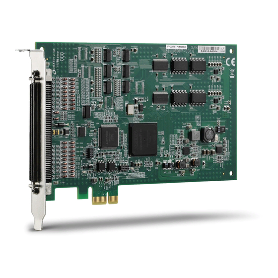
PCIe-7300A
ADLINK Technology PCIe-7300A Manuals
Manuals and User Guides for ADLINK Technology PCIe-7300A. We have
1
ADLINK Technology PCIe-7300A manual available for free PDF download: User Manual
ADLINK Technology PCIe-7300A User Manual (114 pages)
80 MB Ultra-High Speed 32-CH Digital I/O Boards
Brand:
ADLINK Technology
| Category:
I/O Systems
| Size: 0 MB
Table of Contents
Table of Contents
5
List of Tables
8
Introduction
11
Applications
12
Features
12
Specifications
13
Software Support
16
Programming Library
16
DAQ-LVIEW Pnp: Labview® Driver
16
PCIS-VEE: HP-VEE Driver
17
Daqbenchtm: Activex Controls
17
Installation
19
What You Have
19
Unpacking
20
Device Installation for Windows Systems
20
Cpci/Pci/Pcie-7300A Layout
21
Figure 2-1: PCI-7300A Layout Diagram
21
Figure 2-2: Cpci-7300A Layout Diagram
22
Figure 2-3: Pcie-7300A Layout Diagram
22
Hardware Installation Outline
23
Connector Pin Assignment
24
Table 2-1: Connector Pin Assignment
24
Figure 2-4: CN1 Pin Assignment
26
Wiring and Termination
27
Termination Board Support
28
Connect with DIN-100S
28
Connect with DIN-502S
28
Registers
29
I/O Port Base Address
30
Table 3-1: I/O Port Base Address
30
DI_CSR: DI Control & Status Register
32
DO_CSR: DO Control & Status Register
34
Auxiliary Digital I/O Register
36
INT_CSR: Interrupt Control and Status Register
37
DI_FIFO: DI FIFO Direct Access Port
38
DO_FIFO: DO External Data FIFO Direct Access Port
39
FIFO_CR: FIFO Almost Empty/Full Register
40
POL_CNTRL: Control Signal Polarity Control Register
41
PLX PCI-9080 DMA Control Registers
42
Operation Theory
43
I/O Configuration
44
Table 4-1: I/O Configuration
44
Block Diagram
45
Figure 4-1: Block Diagram
45
Digital I/O Data Flow
46
Figure 4-2: Data Flow of Digital Input
46
Figure 4-3: Data Flow of Digital Output
46
Input FIFO and Output FIFO
47
Bus-Mastering DMA
48
Figure 4-4: Maximum Data Throughput
48
Scatter/Gather DMA
50
Figure 4-5: Scatter/Gather DMA for Digital Output
50
Clocking Mode
51
Figure 4-6: Timer Configuration
51
Starting Mode
53
Active Terminator
54
Digital Input Operation Mode
55
Digital Input DMA in Internal Clock Mode
55
Digital Input DMA in External Clock Mode
57
Figure 4-7: DIREQ as Input Data Strobe (Rising Edge Active)
58
Digital Input DMA in Handshaking Mode
59
Figure 4-8: DIREQ as Input Data Strobe (Falling Edge Active)
59
Continuous Digital Input
61
Figure 4-9: DIREQ & DIACK Handshaking
61
Digital Output Operation Mode
63
Digital Output DMA in Internal Clock Mode
63
Digital Output DMA in Handshaking Mode
64
Figure 4-10: DOREQ as Output Data Strobe
64
Digital Output DMA in Burst Handshaking Mode
66
Figure 4-11: DOREQ & DOACK Handshaking
66
Pattern Generator
69
Auxiliary DIO
70
C++ Libraries
71
Libraries Installation
72
Programming Guide
73
Table 5-1: Data Types
73
7300_Initial
74
7300_Close
76
7300_Configure
77
7300_Di_Mode
79
7300_Do_Mode
80
7300_Aux_Di
82
7300_Aux_Di_Channel
83
7300_Aux_Do
84
7300_Aux_Do_Channel
85
7300_Alloc_Dma_Mem
86
7300_Free_Dma_Mem
87
7300_Di_Dma_Start
88
7300_Di_Dma_Status
92
7300_Di_Dma_Abort
93
7300_Getoverrunstatus
94
7300_Do_Dma_Start
95
7300_Do_Dma_Status
97
7300_Do_Dma_Abort
98
7300_Do_Pg_Start
99
7300_Do_Pg_Stop
101
7300_Di_Timer
102
7300_Do_Timer
103
7300_Int_Timer
104
7300_Get_Sample
105
7300_Set_Sample
106
7300_Getunderrunstatus
107
Appendix
109
The Intel (NEC) 8254
109
The Control Byte
109
Mode Definition
111
Advertisement
Advertisement
Related Products
ADLINK Technology PCIe-7256
ADLINK Technology PCIe-7396
ADLINK Technology pci-6308
ADLINK Technology PCI-7300A
ADLINK Technology PCI-7443
ADLINK Technology PCI-7444
ADLINK Technology PCI-7432
ADLINK PCI-7433
ADLINK PCI-7434
ADLINK Technology PCI-725 Series
ADLINK Technology Categories
Computer Hardware
Motherboard
PCI Card
Control Unit
Desktop
More ADLINK Technology Manuals
Login
Sign In
OR
Sign in with Facebook
Sign in with Google
Upload manual
Upload from disk
Upload from URL