Table of Contents
Advertisement
Quick Links
Download this manual
See also:
User Manual
Advertisement
Table of Contents

Related Manuals for ADLINK Technology pci-6308


Summary of Contents for ADLINK Technology pci-6308
- Page 1 ® ® NuIPC / NuDAQ 743X Series 64-CH Isolated Digital I/O Board User’s Guide...
- Page 2 @Copyright 1998~2000 ADLINK Technology Co., Ltd. All Rights Reserved. Manual Rev. 3.10: April 10, 2000 The information in this document is subject to change without prior notice in order to improve reliability, design and function and does not represent a commitment on the part of the manufacturer.
- Page 3 Getting service from ADLINK ♦ Customer Satisfaction is always the most important thing for ADINLK Tech Inc. If you need any help or service, please contact us and get it. ADLINK Technology Inc. Web Site http://www.Adlink.com.tw Sales & Service service@Adlink.com.tw...
-
Page 5: Table Of Contents
Table of Contents How to Use This Guide ..........iii Chapter 1 Introduction..........1 Features ................2 Applications ............... 2 Specifications..............3 Software Supporting............4 1.4.1 Programming Library..............4 ® 1.4.2 PCIS-LVIEW: LabVIEW Driver ...........4 1.4.3 PCIS-VEE: HP-VEE Driver.............5 1.4.4 DAQBench : ActiveX Controls ..........5 1.4.5 PCIS-DDE: DDE Server and InTouch ........5... - Page 6 Digital Input Register............18 Digital Output Register............. 19 Chapter 4 Operation Theorem .........20 Isolated Digital Input Channels......... 20 Isolated Digital Output Channels........21 Chapter 5 C/C++ Libraries........22 Libraries Installation............22 Programming Guide ............22 5.2.1 Naming Convention..............22 5.2.2 Data Types..................23 Running Testing Utility .............
-
Page 7: How To Use This Guide
How to Use This Guide This manual is designed to help you use the 743X series products. It describes how to modify and control various functions on the 743X card to meet your requirements. It is divided into four chapters: •... -
Page 9: Chapter 1 Introduction
Introduction The 743X series products are 64-CH high-density isolated digital input and/or output products. The 743X series products include the following cards which are in different form factor. The following items are for PCI bus products: • PCI-7432: Isolated 32-CH DI and 32-CH DO card •... -
Page 10: Features
The 743X series products use PCI-9050 PCI controller to interface the board to the PCI bus. The PCI-9050 fully implements the PCI local bus specification Rev 2.1. All bus relative configurations, such as base memory and interrupt assignment, are automatically controlled by BIOS software. -
Page 11: Specifications
Specifications ♦ Optical Isolated Input Channel Numbers of Channel: 32 digital inputs for 7432 64 digital inputs for 7433 Input Voltage: 0 - 24V dc 8Logic H: 3~24V 8Logic L: 0~2.4V Input resistance: 2.4KΩ @ 0.5W Isolated voltage: 5000 Vrms Throughput: 10K Hz (0.1 ms) ♦... -
Page 12: Software Supporting
8cPCI-7433[R]: +5V @ 500 mA typical 8cPCI-7434[R][P]: +5V @ 560 mA typical • Dimension: 8PCI-7432/33/34: Compact size only 98mm(H) X 173mm(L) 8cPCI-7432/33/34: Standard 3U CompactPCI form factor 8cPCI-7433R/34R: Standard 3U CompactPCI form factor with rear I/O Software Supporting ADLink provides versatile software drivers and packages for users’ different approach to built-up a system. -
Page 13: Pcis-Vee: Hp-Vee Driver
PCIS-LVIEW contains the VIs, which are used to interface with NI’s ® LabVIEW software package. The PCIS-LVIEW supports Windows ® 95/98/NT/2000. The LabVIEW drivers are free shipped with the board. You can install and use them without license. For detail information about PCIS-LVIEW, please refer to the user’s guide in the CD. -
Page 14: Chapter 2 Installation
Installation This chapter describes how to install the 743X products. Please follow the follow steps to install the PCI-6308 family products. w Check what you have (section 2.1) w Unpacking (section 2.2) w Check the PCB (section 2.3) w Install the hardware (section 2.4) w Install the software drivers and run utility to test (section 2.5) -
Page 15: Unpacking
Unpacking Your PCI-7432/33/34 card contains sensitive electronic components that can be easily damaged by static electricity. The card should be done on a grounded anti-static mat. The operator should be wearing an anti-static wristband, grounded at the same point as the anti-static mat. Inspect the card module carton for obvious damage. -
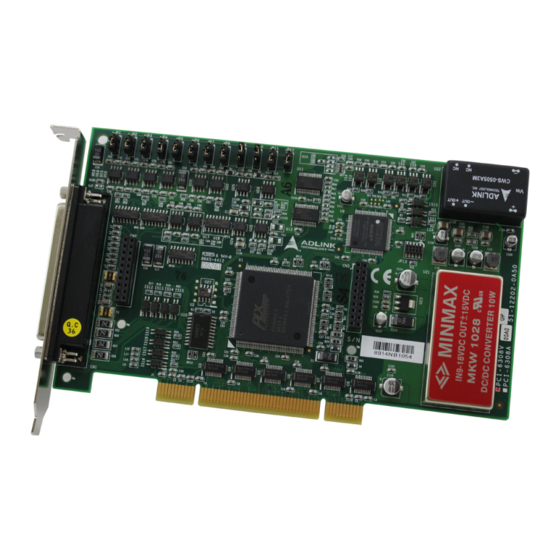
Page 16: Pcb Layout
PCB Layout 2.3.1 PCI-743X PCB Layout The CN1 is for the I/O interface. It is a 100-pin SCSI-type connector. PCI Controller 2.3.2 cPCI-743X PCB Layout The CN1 is for the I/O interface. It is a 100-pin SCSI-type connector. PCI Controller 8 •... -
Page 17: Cpci-743Xr Pcb Layout
2.3.3 cPCI-743XR PCB Layout The CN1 is for the I/O interface. It is a 100-pin SCSI-type connector. The J2 is for rear I/O signal. There is no connector on the main board. PCI Controller Hardware Installation Outline PCI configuration The PCI cards (or CompactPCI cards) are equipped with plug and play PCI controller, it can request base addresses and interrupt according to PCI standard. -
Page 18: Device Installation For Windows Systems
do not touch the components. Position the board into the PCI slot you selected. Secure the card in place at the rear panel of the system. For cPCI-743X (both with and without rear I/O) products, Read through this manual, and setup the jumper according to your application. -
Page 19: Connector Pin Assignment Of Cpci/Pci-7432
Connector Pin Assignment of cPCI/PCI-7432 The pin assignment of the 100 pins SCSI-II connector is an isolated signal connector, 7432’s pin assignment is as shown in Figure 2.7. (51) (1) IDI_0 (26) IDO_0 (51) IDI_8 (76) IDO_8 (52) (2) IDI_1 (27) IDO_1 (52) IDI_9 (77) IDO_9... -
Page 20: Connector Pin Assignment Of Cpci/Pci-7433
Connector Pin Assignment of cPCI/PCI-7433 The pin assignment of the 100 pins SCSI-II connector is an isolated signal connector, 7433’s pin assignment is as shown in Figure 2.8. (51) (1) IDI_0 (26) IDI_32 (51) IDI_8 (76) IDI_40 (52) (2) IDI_1 (27) IDI_33 (52) IDI_9 (77) IDI_41... -
Page 21: Connector Pin Assignment Of Pci-7434
Connector Pin Assignment of PCI-7434 The pin assignment of the 100 pins SCSI-II connector is an isolated signal connector, PCI-7434’s pin assignment is as shown in Figure 2.9. (51) (1) IDO_0 (26) IDO_32 (51) IDO_8 (76) IDO_40 (52) (53) (2) IDO_1 (27) IDO_33 (52) IDO_9 (77) IDO_41 (3) IDO_2... -
Page 22: Connector Pin Assignment Of Cpci-7434[R]
Connector Pin Assignment of cPCI-7434[R] Since cPCI-7434[R]’s pin assignment is as shown in Figure 2.10. (51) (1) IDO_0 (26) IDO_32 (51) IDO_8 (76) IDO_40 (52) (53) (2) IDO_1 (27) IDO_33 (52) IDO_9 (77) IDO_41 (3) IDO_2 (28) IDO_34 (53) IDO_10 (78) IDO_42 (4) IDO_3 (29) IDO_35 (54) IDO_11 (79) IDO_43 (5) IDO_4... -
Page 23: 2.10 Connector Pin Assignment Of Cpci-7434[R]P
2.10 Connector Pin Assignment of cPCI-7434[R]P Since cPCI-7434[R]P’s pin assignment is as shown in Figure 2.11. (51) (1) IDO_0 (26) IDO_32 (51) IDO_8 (76) IDO_40 (52) (53) (2) IDO_1 (27) IDO_33 (52) IDO_9 (77) IDO_41 (3) IDO_2 (28) IDO_34 (53) IDO_10 (78) IDO_42 (4) IDO_3 (29) IDO_35 (54) IDO_11 (79) IDO_43 (5) IDO_4... -
Page 24: Chapter 3 Registers Format
The PCI PnP BIOS assigns the base address of the LCR. The assigned address is located at offset 14h of PCR. The PCI-6308 registers are shown in the next section. The base address, which is also assigned by the PCI PnP BIOS, is located at offset 18h of PCR. -
Page 25: I/O Address Map
I/O Address Map The 743X board registers are in 32-bit width. The users can access these registers by only 32-bit I/O instructions. The following tables show the address map, including descriptions and their offset addresses relative to the base address. Address Write Read... -
Page 26: Digital Input Register
Digital Input Register There are 32 isolated digital input channels on PCI-7432 and 64 isolated digital input channels on the PCI-7433, each bit of based address is corresponding to a signal on the digital input channel. Address : BASE + 0 ~ BASE + 3 for 7432 BASE + 0 ~ BASE + 7 for 7433 Attribute : read only Data Format :... -
Page 27: Digital Output Register
Digital Output Register There are total 32 digital output channels on the PCI-7432 and 64 isolated digital input channels on the PCI-7434, each bit of based address is corresponding to a signal on the digital output channel. Address: BASE + 0 ~ BASE + 3 for 7432 BASE + 0 ~ BASE + 7 for 7434 Attribute : write only Data Format :... -
Page 28: Chapter 4 Operation Theorem
Operation Theorem Isolated Digital Input Channels The isolated digital input is open collector transistor structure. The input voltage range form 0V to 24V and input resister is 2.4KΩ. The connection between outside signal and 7432/33 is shown in Fig 4.1. Please note that the input common junction could be common ground or common power, they are dependent on the user’s environment. -
Page 29: Isolated Digital Output Channels
Isolated Digital Output Channels The common ground connection of isolated digital output is shown as figure 4.2, while common power connection of isolated digital output as figure 4.3. When the isolated digital output goes “ON”, the sink current will be conducted through the transistors. When the isolated digital output goes “OFF”, no current could flow through the transistor. -
Page 30: Chapter 5 C/C++ Libraries
C/C++ Libraries This chapter describes the software library for operating this card. Only the functions in DOS library and Windows 95 DLL are described. Please refer to the PCIS-DASK function reference manual, which included in ADLINK CD, for the descriptions of the Windows 98/NT/2000 DLL functions. -
Page 31: Data Types
In DOS Environment : _{hardware_model}_{action_name}. e.g. _7432_Initial() . All functions in PCI-7432 driver are with 7432 as {hardware_model}. But they can be used by PCI-7432 and cPCI-7432. All functions in PCI-7433 driver are with 7433 as {hardware_model}. But they can be used by PCI-7433, cPCI-7433 and cPCI-7433R. -
Page 32: Initial
Initial @ Description The 743X cards are initialized by this function. The software library could be used to control multiple 743X cards. Because PCI-743X is in PCI bus architecture and meets the plug and play specifications, the IRQ and I/O address are assigned by system BIOS directly. -
Page 33: Digital Input Relative Functions
Digital Input Relative Functions @ Description These functions are used to read 32-bit digital inputs data from digital input port. You can get 32 bits data from 7432 by using function “_7432_DI”, get 32 bits data (MSB double word) from 7433 by using “7433_DI_HiDW”, get 32 bits data (LSB double word) from PCI-7433 by using “7433_DI_LoDW”. -
Page 34: Digital Output Relative Functions
Digital Output Relative Functions @ Description These functions are used to write data to digital output ports. You can write 32 bits data to 7432 by using function “_7432_DO”; write 32 bits data (MSB double word) to 7434 by using “7434_DO_HiDW”; or write 32 bits data (LSB double word) to 7434 by using “7434_DO_LoDW”. -
Page 35: Interrupt Source Control
Interrupt Source Control @ Description The 7432 or 7433 has dual interrupts system, two interrupt sources can be generated and be checked by the software. This function is used to select and control 7432/33 interrupt sources by writing data to interrupt control register. -
Page 36: Get Interrupt Status
Get Interrupt Status @ Description The PCI-7432 or PCI-7433 has dual interrupts system. Two interrupt sources can be generated and be checked by the software. This function is used to distinguish which interrupt is inserted if both INT1 and INT2 interrupts are used. @ Syntax PCI-7432 / cPCI-7432 C/C++ (DOS) -
Page 37: Interrupt Enable
Interrupt Enable @ Description This function is only available in Windows 95 driver. This function is used to start up the interrupt control. After calling this function, every time an interrupt request is generated, a software event is signaled. So that in your program, you can use wait operation to wait for the event. -
Page 38: 5.10 Interrupt Disable
5.10 Interrupt Disable @ Description This function is only available in Windows 95 driver. This function is used to disable the interrupt signal generation. @ Syntax PCI-7432 / cPCI-7432 C/C++ (Windows 95) W_7432_INT_Disable (U16 cardNo) Visual Basic (Windows 95) W_7432_INT_Disable (ByVal cardNo As Integer) As Integer PCI-7433 / cPCI-7433 / cPCI-7433R C/C++ (Windows 95) W_7433_INT_DIsable (U16 cardNo) -
Page 39: 5.11 Led Control Function
5.11 LED Control Function @ Description The LED control function is only available on the CompactPCI rear I/O version. The cPCI-7433R/34R has four user defined LED lights. This function is used to control the LED lights. @ Syntax cPCI-7433R / cPCI-7434R C/C++ (DOS) void _7433R_LED (U16 cardNo, U32 LED_Data) -
Page 40: 5.12 Get Slot Number
5.12 Get Slot Number @ Description The Get slot number function is only available on the CompactPCI rear I/O version. The slot number is read back from the Geographic address which defined on the backplane. @ Syntax cPCI-7433R / cPCI-7434R C/C++ (DOS) void _7433R_SlotNo (U16 cardNo, U32 *slot_No) -
Page 41: Product Warranty/Service
Product Warranty/Service Seller warrants that equipment furnished will be free form defects in material and workmanship for a period of one year from the confirmed date of purchase of the original buyer and that upon written notice of any such defect, Seller will, at its option, repair or replace the defective item under the terms of this warranty, subject to the provisions and specific exclusions listed herein.
Need help?
Do you have a question about the pci-6308 and is the answer not in the manual?
Questions and answers