ADLINK Technology cPCI-7300A Manuals
Manuals and User Guides for ADLINK Technology cPCI-7300A. We have 3 ADLINK Technology cPCI-7300A manuals available for free PDF download: User Manual
ADLINK Technology cPCI-7300A User Manual (112 pages)
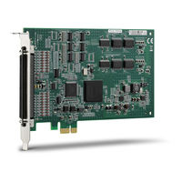
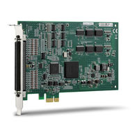
80MB Ultra-High Speed 32-CH
Digital I/O Boards
Brand: ADLINK Technology
|
Category: I/O Systems
|
Size: 0 MB
Table of Contents
Advertisement
ADLINK Technology cPCI-7300A User Manual (114 pages)
80 MB Ultra-High Speed 32-CH Digital I/O Boards
Brand: ADLINK Technology
|
Category: I/O Systems
|
Size: 0 MB
Table of Contents

ADLINK Technology cPCI-7300A User Manual (85 pages)
80MB Ultra-High Speed 32-CH Digital I/O Boards
Brand: ADLINK Technology
|
Category: Computer Hardware
|
Size: 4 MB
Table of Contents
Advertisement