Renesas RH850/F1x User Manual
Piggyback board v1
Hide thumbs
Also See for RH850/F1x:
- User manual (25 pages) ,
- User manual (28 pages) ,
- User manual (44 pages)
Table of Contents
Advertisement
Quick Links
RH850 Evaluation Platform
RH850/F1x 64pin
RH850/F1Kx 64pin
32
PiggyBack board V1
Y-RH850-F1X-064PIN-PB-T1-V1
All information contained in these materials, including products and product specifications,
represents information on the product at the time of publication and is subject to change by
Renesas Electronics Corp. without notice. Please review the latest information published by
Renesas Electronics Corp. through various means, including the Renesas Technology Corp.
website (http://www.renesas.com).
The newest version of this document can be obtained from the following web location
http://www.renesas.eu/updates?oc=Y-RH850-F1X-064PIN-PB-T1-V1
www.renesa s.com
R20UT2767ED0130, Rev. 1.30
2018-11-23
Advertisement
Table of Contents

Subscribe to Our Youtube Channel
Related Manuals for Renesas RH850/F1x


Summary of Contents for Renesas RH850/F1x
- Page 1 All information contained in these materials, including products and product specifications, represents information on the product at the time of publication and is subject to change by Renesas Electronics Corp. without notice. Please review the latest information published by Renesas Electronics Corp. through various means, including the Renesas Technology Corp.
- Page 2 You may not use any Renesas Electronics product for any application for which it is not intended. Renesas Electronics shall not be in any way liable for any damages or losses incurred by you or third parties arising from the use of any Renesas Electronics product for which the product is not intended by Renesas Electronics.
- Page 3 General Precautions in the Handling of Microprocessing Unit and Microcontroller Unit Products The following usage notes are applicable to all Microprocessing unit and Microcontroller unit products from Renesas. For detailed usage notes on the products covered by this document, refer to the relevant sections of the document as well as any technical updates that have been issued for the products.
-
Page 4: Table Of Contents
Table of Contents Chapter 1 Introduction ................. 5 Chapter 2 Overview ................6 Overview ....................6 Mounting of the device ................ 7 Chapter 3 Power supply ............... 8 Board power connections ..............8 Voltage distribution ................9 Chapter 4 Clock sources ..............10 4.1.1 MainOsc ........................ -
Page 5: Chapter 1 Introduction
Chapter 1 Introduction The RH850/F1x Application Board is part of the RH850 Evaluation Platform and serves as a simple and easy to use platform for evaluating the features and performance of Renesas Electronics 32-bit RH850/F1x microcontrollers. The piggyback board (Y-RH850-F1X-064PIN-PB-T1-V1) can be used as a standalone board, or can be mated with a mainboard (e.g. -
Page 6: Chapter 2 Overview
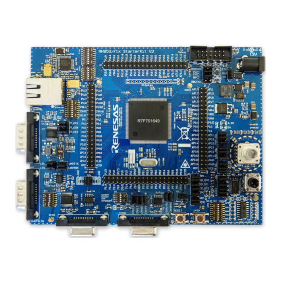
Chapter 2 Overview Overview Figures 1 and 2 provide the views of the Piggyback Board. Device pin #1 Figure 1 – PiggyBoard top view Figure 2 – PiggyBoard bottom view R20UT2767ED0130 Rev.1.30 2018-11-23... -
Page 7: Mounting Of The Device
Mounting of the device The board is designed for use with the following device: • RH850/F1L 64pin • RH850/F1KM-S1 64pin The device must be placed inside the socket IC1. To insert the device, press down the lid, align the #1 pin of the device to the #1pin of the socket, insert the device inside the socket and release the lid. -
Page 8: Chapter 3 Power Supply
Chapter 3 Power supply Board power connections For operation of the device, a supply voltage must be connected to the board. Though a single supply voltage is sufficient for the operation of the device, two (different) voltages can be supplied to the board. Within this document the following voltages are considered as ‘typical’... -
Page 9: Voltage Distribution
Voltage distribution The table shows the required device power supply pins and their function: Device supply pin Function REGVDD Supply for the device internal regulators for the digital logic. EVDD Supply for ports of AWO and ISO area. A0VREF Supply for ports and analog functions of ADC0. Additionally one power supply for MainBoard can be selected: Supply voltage Function... -
Page 10: Chapter 4 Clock Sources
Chapter 4 Clock sources 4.1.1 MainOsc A crystal or ceramic resonator in the range of 8MHz to 24MHz can be mounted on socket X1. A 8MHz and 16Mhz oscillator is supplied with the board. R20UT2767ED0130 Rev.1.30 2018-11-23... -
Page 11: Chapter 5 Debug And Programming Interface
Chapter 5 Debug and Programming interface For connection of the microcontroller debug and flash programming tools, the connector CN19 is provided. The signal connection of the connector CN19 is shown in the picture below: CN19 pin Device Port Device signal JP0_2 DCUTCK / LPDCLK JP0_4... -
Page 12: Chapter 6 Connectors For Ports Of Device
Chapter 6 Connectors for ports of device Connection to each pin of the device is possible via the connectors CN5 to CN8. Note :The pin headers are directly connected to the pins, therefore special care must be taken to avoid any electrostatic or other damage to the device. Push button for RESET In order to issue a RESET to the device, the push-button SW1 is available. - Page 13 FLX1TX FLX1EN FLX1RX ETH0MDIO ETH0MDC ETH0RXD0 EH0TXD0 ETH0RXD1 EH0TXD1 ETH0RXD2 EH0TXD2 ETH0RXD3 EH0TXD3 ETH0RXDCLK ETH0TXCLK ETH0RXER ETH0TXER ETH0CRSDV ETH0TXEN ETH0RXDV ETH0COL ETH0RESET USB0UDMF USB0UDMH USB0UDPF USB0UDPH DIGIO_0 P8_0 DIGIO_1 P8_1 DIGIO_2 P8_2 DIGIO_3 P8_3 DIGIO_4 P8_4 DIGIO_5 P8_5 DIGIO_6 P8_6 DIGIO_7 P0_0 DIGIO_8...
-
Page 14: Connector Cn2
6.2.2 Connector CN2 Function Device Port Function Device Port CAN2Tx CAN3Tx CAN2Rx CAN3Rx CAN4Tx CAN5Tx CAN4Rx CAN5Rx LIN2Tx LIN3Tx LIN2Rx LIN3Rx LIN4Tx LIN5Tx LIN4Rx LIN5Rx LIN6Tx LIN7Tx LIN6Rx LIN7Rx LIN8Tx LIN9Tx LIN8Rx LIN9Rx LIN10Tx LIN11Tx P10_10 P0_5 LIN10Rx LIN11Rx P10_9 P0_4 LIN12Tx LIN13Tx... -
Page 15: Connector Cn3
6.2.3 Connector CN3 Function Device Port Function Device Port P10_0 P10_1 PWM00 PWM01 PWM02 P10_2 P10_3 PWM03 PWM04 P10_7 P10_8 PWM05 PWM06 P10_9 P10_10 PWM07 PWM08 P9_0 P9_1 PWM09 PWM10 P0_4 P0_1 PWM11 PWM12 P0_2 P0_3 PWM13 PWM14 P8_0 PWM15 P8_1 PWM16 P10_11... - Page 16 PWM37 PWM36 PWM39 PWM38 PWM41 PWM40 PWM43 PWM42 PWM44 PWM45 PWM46 PWM47 PWM48 PWM49 PWM50 PWM51 PWM52 PWM53 PWM54 PWM55 PWM56 PWM57 PWM58 PWM59 PWM60 PWM61 PWM62 PWM63 PWM64 PWM65 PWM66 PWM67 PWM68 PWM69 PWM70 PWM71 PWM72 PWM73 PWM74 PWM75 PWM76 PWM77 PWM78...
-
Page 17: Chapter 7 Mechanical Dimensions
Chapter 7 Mechanical dimensions 100,00mm R20UT2767ED0130 Rev.1.30 2018-11-23... -
Page 18: Chapter 8 Schematic
Chapter 8 Schematic R20UT2767ED0130 Rev.1.30 2018-11-23... - Page 19 PUSH BUTTON 4 PIN SMD R20UT2767ED0130 Rev.1.30 2018-11-23...
- Page 20 R20UT2767ED0130 Rev.1.30 2018-11-23...
-
Page 21: Chapter 9 Revision History
Chapter 9 Revision History The table provides information about the major changes of the document versions. Date Version Description 2013-11-05 Initial release 2014-06-10 Updated cover page Updated schematic for improved readability (same content) 2015-10-21 Updated description and schematic in chapter 3.2 Updated description of CN19, pin 6, chapter 5 2018-11-23 1.30...
Need help?
Do you have a question about the RH850/F1x and is the answer not in the manual?
Questions and answers