Renesas RH850/F1x User Manual
Piggyback board v3
Hide thumbs
Also See for RH850/F1x:
- User manual (28 pages) ,
- User manual (44 pages) ,
- User manual (21 pages)
Table of Contents
Advertisement
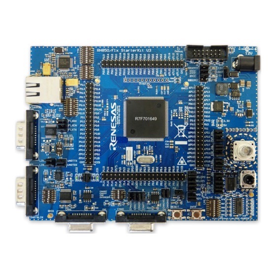
RH850 Evaluation Platform
RH850/F1x 144-pin
RH850/R1x 144-pin
32
PiggyBack board V3
Y-RH850-F1X-144PIN-PB-T1-V3
All information contained in these materials, including products and product specifications,
represents information on the product at the time of publication and is subject to change by
Renesas Electronics Corp. without notice. Please review the latest information published by
Renesas Electronics Corp. through various means, including the Renesas Technology Corp.
website (http://www.renesas.com).
The newest version of this document can be obtained from the following web location
http://www.renesas.eu/updates?oc=Y-RH850-F1X-144PIN-PB-T1-V3
www.renesa s.com
R20UT4129ED0100, Rev. 1.00
2017-06-21
Advertisement
Table of Contents

Related Manuals for Renesas RH850/F1x


Summary of Contents for Renesas RH850/F1x
- Page 1 All information contained in these materials, including products and product specifications, represents information on the product at the time of publication and is subject to change by Renesas Electronics Corp. without notice. Please review the latest information published by Renesas Electronics Corp. through various means, including the Renesas Technology Corp.
- Page 2 You may not use any Renesas Electronics product for any application for which it is not intended. Renesas Electronics shall not be in any way liable for any damages or losses incurred by you or third parties arising from the use of any Renesas Electronics product for which the product is not intended by Renesas Electronics.
- Page 3 General Precautions in the Handling of Microprocessing Unit and Microcontroller Unit Products The following usage notes are applicable to all Microprocessing unit and Microcontroller unit products from Renesas. For detailed usage notes on the products covered by this document, refer to the relevant sections of the document as well as any technical updates that have been issued for the products.
-
Page 4: Table Of Contents
User’s Manual Y-RH850-F1X-144PIN-PB-T1-V3 Table of Contents Chapter 1 Introduction ................. 5 Chapter 2 Overview ................6 Overview ....................6 Mounting of the device ................ 7 Chapter 3 Jumper Configuration ............8 Chapter 4 Power supply ..............10 Board power connection ..............10 Voltage distribution ................ -
Page 5: Chapter 1 Introduction
User’s Manual Y-RH850-F1X-144PIN-PB-T1-V3 Chapter 1 Introduction The RH850/F1x Application Board is part of the RH850 Evaluation Platform and serves as a simple and easy to use platform for evaluating the features and performance of Renesas Electronics 32-bit RH850/F1x microcontrollers. The piggyback board (Y-RH850-F1X-144PIN-PB-T1-V3) can be used as a standalone board, or can be mated with a mainboard (e.g. -
Page 6: Chapter 2 Overview
User’s Manual Y-RH850-F1X-144PIN-PB-T1-V3 Chapter 2 Overview Overview Figures 1 and 2 provide the views of the Piggyback Board. Device pin #1 Figure 1 – PiggyBoard top view Figure 2 – PiggyBoard bottom view R20UT4129ED0100 Rev.1.00 2017-06-21... -
Page 7: Mounting Of The Device
User’s Manual Y-RH850-F1X-144PIN-PB-T1-V3 Mounting of the device The board is designed for use with the following devices, all in their 144 pin package: RH850/F1L RH850/F1M RH850/F1K RH850/F1KM-S4 RH850/R1L The device must be placed inside the socket IC1. To insert the device, press down the lid, align the #1 pin of the device to the #1pin of the socket, insert the device inside the socket and release the lid. -
Page 8: Chapter 3 Jumper Configuration
User’s Manual Y-RH850-F1X-144PIN-PB-T1-V3 Chapter 3 Jumper Configuration The function of the board can be configured via jumpers. This chapter describes the standard configuration, i.e. jumper setting for the intended devices. For the supported function of the used device, please refer to the corresponding HW user’s manual. - Page 9 User’s Manual Y-RH850-F1X-144PIN-PB-T1-V3 The jumper setting also are shown in this picture: Figure 3 – Jumper setting overview green jumper JP12 for FLMDO0 always must be closed for a ‘normal’ (user mode and debug) operation of the device. must be set for a single “Voltage 1”...
-
Page 10: Chapter 4 Power Supply
User’s Manual Y-RH850-F1X-144PIN-PB-T1-V3 Chapter 4 Power supply Board power connection For operation of the device, a supply voltage must be connected to the board. Though a single supply voltage is sufficient for the operation of the device, two (different) voltages can be supplied to the board. Within this document the following voltages are considered as ‘typical’... -
Page 11: Voltage Distribution
User’s Manual Y-RH850-F1X-144PIN-PB-T1-V3 Voltage distribution The table shows the required device power supply pins and their function: Device supply pin Function Supply for the device internal regulators for the digital REGVCC logic. EVCC Supply for ports of AWO and ISO area. BVCC Supply for ports of AWO and ISO area. -
Page 12: Chapter 5 Clock Sources
User’s Manual Y-RH850-F1X-144PIN-PB-T1-V3 Chapter 5 Clock sources Four external crystal oscillators for the device clock supply are provided with the board. 5.1.1 MainOsc A crystal or ceramic resonator in the range of 8MHz to 24MHz can be mounted on socket X1. A 8MHz, 16Mhz and 20MHz oscillator is supplied with the board. -
Page 13: Chapter 6 Debug And Programming Interface
User’s Manual Y-RH850-F1X-144PIN-PB-T1-V3 Chapter 6 Debug and Programming interface For connection of the microcontroller debug and flash programming tools, the connector CN19 is provided. The signal connection of the connector CN19 is shown in the picture below: CN19 pin Device Port Device signal JP0_2 DCUTCK / LPDCLK... -
Page 14: Chapter 7 Connectors For Ports Of Device
User’s Manual Y-RH850-F1X-144PIN-PB-T1-V3 Chapter 7 Connectors for ports of device Connection to each pin of the device is possible via the connectors CN5 to CN8. Note :The pin headers are directly connected to the pins, therefore special care must be taken to avoid any electrostatic or other damage to the device. Push button for RESET In order to issue a RESET to the device, the push-button SW1 is available. - Page 15 User’s Manual Y-RH850-F1X-144PIN-PB-T1-V3 USB0UDPF USB0UDPH DIGIO_0 P8_0 DIGIO_1 P8_1 DIGIO_2 P8_2 DIGIO_3 P8_3 DIGIO_4 P8_4 DIGIO_5 P8_5 DIGIO_6 P8_6 DIGIO_7 P11_0 DIGIO_8 P10_0 DIGIO_9 P10_7 DIGIO_10 P10_8 DIGIO_11 P10_15 DIGIO_12 P0_9 DIGIO_13 P0_10 DIGIO_14 P0_11 DIGIO_15 P0_12 103 MUX0 P10_4 MUX1 P10_5 105 MUX2...
-
Page 16: Connector Cn2
User’s Manual Y-RH850-F1X-144PIN-PB-T1-V3 7.2.2 Connector CN2 Function Device Port Function Device Port CAN2Tx P12_0 CAN3Tx P1_3 CAN2Rx P11_15 CAN3Rx P1_2 CAN4Tx P0_10 CAN5Tx P11_6 CAN4Rx P0_9 CAN5Rx P11_5 LIN2Tx P0_10 LIN3Tx P20_5 11 LIN2Rx P0_9 LIN3Rx P20_4 13 LIN4Tx P1_11 LIN5Tx P11_11 15 LIN4Rx... - Page 17 User’s Manual Y-RH850-F1X-144PIN-PB-T1-V3 R20UT4129ED0100 Rev.1.00 2017-06-21...
-
Page 18: Connector Cn3
User’s Manual Y-RH850-F1X-144PIN-PB-T1-V3 7.2.3 Connector CN3 Function Device Port Function Device Port PWM00 P10_0 PWM01 P10_1 PWM02 P10_2 PWM03 P10_3 PWM04 P10_7 PWM05 P10_8 PWM06 P10_9 PWM07 P10_10 PWM08 P9_0 PWM09 P9_1 PWM10 P0_4 PWM11 P0_1 PWM12 P0_2 PWM13 P0_3 PWM14 P8_0 PWM15... - Page 19 User’s Manual Y-RH850-F1X-144PIN-PB-T1-V3 PWMADC10 AP1_2 PWMADC1 AP1_3 PWMADC12 AP1_4 PWMADC1 AP1_5 PWMADC14 AP1_6 PWMADC1 AP1_7 R20UT4129ED0100 Rev.1.00 2017-06-21...
-
Page 20: Chapter 8 Other Circuitry
User’s Manual Y-RH850-F1X-144PIN-PB-T1-V3 Chapter 8 Other circuitry Push button for RESET In order to issue a RESET to the device, the push-button SW1 is available. Mode Selection The PiggyBack Board gives the possibility to configure the following mode pins FLMD0 via jumper JP12 ... -
Page 21: Chapter 9 Mechanical Dimensions
User’s Manual Y-RH850-F1X-144PIN-PB-T1-V3 Chapter 9 Mechanical dimensions 100,00mm 50,00mm R20UT4129ED0100 Rev.1.00 2017-06-21... -
Page 22: Chapter 10 Schematic
User’s Manual Y-RH850-F1X-144PIN-PB-T1-V3 Chapter 10 Schematic R20UT4129ED0100 Rev.1.00 2017-06-21... - Page 23 User’s Manual Y-RH850-F1X-144PIN-PB-T1-V3 PUSH BUTTON 4 PIN SMD R20UT4129ED0100 Rev.1.00 2017-06-21...
- Page 24 User’s Manual Y-RH850-F1X-144PIN-PB-T1-V3 R20UT4129ED0100 Rev.1.00 2017-06-21...
-
Page 25: Chapter 11 Revision History
User’s Manual Y-RH850-F1X-144PIN-PB-T1-V3 Chapter 11 Revision History The table provides information about the major changes of the document versions. Date Version Description 2017-06-21 Initial release Differences to the Y-RH850-F1X-144PIN-PB-T1-V2: Support for RH850/F1K and F1KM-S4 devices. Added jumpers for mode selection. ...
Need help?
Do you have a question about the RH850/F1x and is the answer not in the manual?
Questions and answers