Sign In
Upload
Manuals
Brands
Renesas Manuals
Power Supply
RH850/F1Kx Series
Renesas RH850/F1Kx Series Manuals
Manuals and User Guides for Renesas RH850/F1Kx Series. We have
2
Renesas RH850/F1Kx Series manuals available for free PDF download: Hardware Design Manual, User Manual
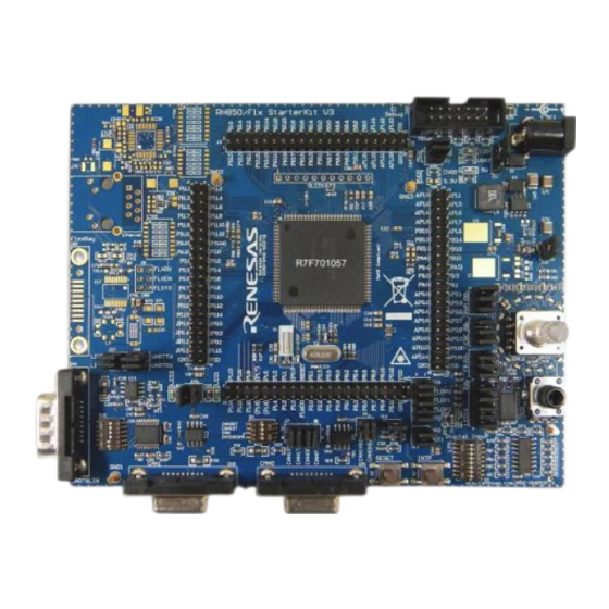
Renesas RH850/F1Kx Series Hardware Design Manual (112 pages)
Brand:
Renesas
| Category:
Power Supply
| Size: 1.76 MB
Table of Contents
Table of Contents
2
Power Supply
8
Power Supply Overview of RH850/F1KM-S1
8
Power Supply Pin Overview of RH850/F1KM-S1
8
Table 1: RH850/F1KM-S1 Power Supply Pin Overview
8
Power Supply Pin Configuration of RH850/F1KM-S1
9
Power Supply Pin Architecture of RH850/F1KM-S1
9
Figure 1: RH850/F1KM-S1 Power Supply Architecture
9
Table 2: RH850/F1KM-S1 Overview of Power Supply Architecture Cases
10
Table 3: RH850/F1KM-S1 Power Supply Architecture with Single Supply 5V
10
Table 4: RH850/F1KM-S1 Power Supply Architecture with Mixed Supply 5V & 3.3V
10
Table 5: RH850/F1KM-S1 Power Supply Architecture with Mixed Supply 5V & 3.3V
11
Table 6: RH850/F1KM-S1 Power Supply Architecture with Mixed Supply 5V & 3.3V
11
Table 7: RH850/F1KM-S1 Power Supply Architecture with Single Supply 3.3V
11
Power Supply Timing of RH850/F1KM-S1
12
Figure 2: Recommended REGVCC Power Configuration for RH850/F1KM-S1
12
Figure 3: the Voltage Range Which Has to be Kept Voltage Slope for RH850/F1KM-S1
12
Figure 4: RH850/F1KM-S1 Power Up/Down Timing
13
Figure 5: RH850/F1KM-S1 Power Up/Down Timing
13
Power Supply Overview of RH850/F1KM-XX
14
Power Supply Overview of RH850/F1KM-S4
15
Power Supply Pin Overview of RH850/F1KM-S4
15
Table 8: RH850/F1KM-S4 Power Supply Pin Overview
15
Power Supply Pin Configuration of RH850/F1KM-S4
16
Power Supply Pin Architecture of RH850/F1KM-S4
16
Figure 6: RH850/F1KM-S4 Power Supply Architecture
16
Table 9: RH850/F1KM-S4 Overview of Power Supply Architecture Cases
17
Table 10: RH850/F1KM-S4 Power Supply Architecture with Single Supply 5V
17
Table 11: RH850/F1KM-S4 Power Supply Architecture with Mixed Supply 5V & 3.3V
18
Table 12: RH850/F1KM-S4 Power Supply Architecture with Mixed Supply 5V & 3.3V
18
Table 13: RH850/F1KM-S4 Power Supply Architecture with Mixed Supply 5V & 3.3V
19
Table 14: RH850/F1KM-S4 Power Supply Architecture with Mixed Supply 5V & 3.3V
20
Table 15: RH850/F1KM-S4 Power Supply Architecture with Mixed Supply 5V & 3.3V
21
Table 16: RH850/F1KM-S4 Power Supply Architecture with Mixed Supply 5V & 3.3V
22
Table 17: RH850/F1KM-S4 Power Supply Architecture with Mixed Supply 5V & 3.3V
23
Table 18: RH850/F1KM-S4 Power Supply Architecture with Mixed Supply 5V & 3.3V
23
Table 19: RH850/F1KM-S4 Power Supply Architecture with Mixed Supply 5V & 3.3V
23
Table 20: RH850/F1KM-S4 Power Supply Architecture with Mixed Supply 5V & 3.3V
24
Table 21: RH850/F1KM-S4 Power Supply Architecture with Mixed Supply 5V & 3.3V
25
Table 22: RH850/F1KM-S4 Power Supply Architecture with Mixed Supply 5V & 3.3V
26
Table 23: RH850/F1KM-S4 Power Supply Architecture with Single Supply 3.3V
26
Power Supply Timing of RH850/F1KM-S4
27
Figure 7: Recommended REGVCC Power Configuration for RH850/F1KM-S4
27
Figure 8: the Voltage Range Which Has to be Kept Voltage Slope for RH850/F1KM-S4
27
Figure 9: RH850/F1KM-S4 Power Up/Down Timing
28
Figure 10: RH850/F1KM-S4 Power Up/Down Timing
28
Power Supply Overview of RH850/F1KH-D8
29
Power Supply Pin Overview of RH850/F1KH-D8
29
Table 24: RH850/F1HM-D8 Power Supply Pin Overview
29
Power Supply Pin Configuration of RH850/F1KH-D8
30
Power Supply Pin Architecture of RH850/F1KH-D8
30
Figure 11: RH850/F1KH-D8 Power Supply Architecture
30
Table 25: RH850/F1KH-D8 Overview of Power Supply Architecture Cases
31
Table 26: RH850/F1KH-D8 Power Supply Architecture with Single Supply 5V
31
Table 27: RH850/F1KH-D8 Power Supply Architecture with Mixed Supply 5V & 3.3V
32
Table 28: RH850/F1KH-D8 Power Supply Architecture with Mixed Supply 5V & 3.3V
32
Table 29: RH850/F1KH-D8 Power Supply Architecture with Mixed Supply 5V & 3.3V
33
Table 30: RH850/F1KH-D8 Power Supply Architecture with Mixed Supply 5V & 3.3V
33
Table 31: RH850/F1KH-D8 Power Supply Architecture with Mixed Supply 5V & 3.3V
34
Table 32: RH850/F1KH-D8 Power Supply Architecture with Mixed Supply 5V & 3.3V
34
Table 33: RH850/F1KH-D8 Power Supply Architecture with Mixed Supply 5V & 3.3V
35
Table 34: RH850/F1KH-D8 Power Supply Architecture with Mixed Supply 5V & 3.3V
36
Table 35: RH850/F1KH-D8 Power Supply Architecture with Mixed Supply 5V & 3.3V
36
Table 36: RH850/F1KH-D8 Power Supply Architecture with Mixed Supply 5V & 3.3V
36
Table 37: RH850/F1KH-D8 Power Supply Architecture with Mixed Supply 5V & 3.3V
37
Table 38: RH850/F1KH-D8 Power Supply Architecture with Mixed Supply 5V & 3.3V
37
Table 39: RH850/F1KH-D8 Power Supply Architecture with Mixed Supply 5V & 3.3V
38
Table 40: RH850/F1KH-D8 Power Supply Architecture with Mixed Supply 5V & 3.3V
39
Table 41: RH850/F1KH-D8 Power Supply Architecture with Mixed Supply 5V & 3.3V
40
Table 42: RH850/F1KH-D8 Power Supply Architecture with Single Supply 3.3V
40
Power Supply Timing of RH850/F1KH-D8
41
Figure 12: Recommended REG0VCC Power Configuration for RH850/F1KH-D8
41
Figure 13: the Voltage Range Which Has to be Kept Voltage Slope for RH850/F1KH-D8
41
Figure 14: RH850/F1KH-D8 Power Up/Down Timing
42
Figure 15: RH850/F1KH-D8 Power Up/Down Timing
43
Power Supply Overview of RH850/F1K
44
Power Supply Pin Overview of RH850/F1K
44
Table 43: RH850/F1K Power Supply Pin Overview
44
Power Supply Pin Configuration of RH850/F1K
45
Power Supply Pin Architecture of RH850/F1K
45
Figure 16: RH850/F1K Power Supply Architecture
45
Table 44: RH850/F1K Overview of Power Supply Architecture Cases
46
Table 45: RH850/F1K Power Supply Architecture with Single Supply 5V
46
Table 46: RH850/F1K Power Supply Architecture with Mixed Supply 5V & 3.3V
46
Table 47: RH850/F1K Power Supply Architecture with Mixed Supply 5V & 3.3V
47
Table 48: RH850/F1K Power Supply Architecture with Mixed Supply 5V & 3.3V
47
Table 49: RH850/F1K Power Supply Architecture with Mixed Supply 5V & 3.3V
47
Table 50: RH850/F1K Power Supply Architecture with Mixed Supply 5V & 3.3V
48
Table 51: RH850/F1K Power Supply Architecture with Mixed Supply 5V & 3.3V
49
Table 52: RH850/F1K Power Supply Architecture with Mixed Supply 5V & 3.3V
50
Table 53: RH850/F1K Power Supply Architecture with Single Supply 3.3V
50
Power Supply Timing of RH850/F1K
51
Figure 17: Recommended REGVCC Power Configuration for RH850/F1K
51
Figure 18: the Voltage Range Which Has to be Kept Voltage Slope for RH850/F1K
51
Figure 19: RH850/F1K Power Up/Down Timing
52
Figure 20: RH850/F1K Power Up/Down Timing
52
Principle Capacitor Placement at REGVCC of Rh850/F1Kx, RH850/F1K Series
53
Figure 21: Principle Capacitor Placement at REGVCC for EMI
53
Minimum External Components
54
Minimum External Components of RH850/F1KM-S1
54
Figure 22: Minimum External Components of RH850/F1KM-S1 in Normal Operating Mode
54
Table 54: Minimum External Components of RH850/F1KM-S1 (100Pin)
55
Minimum External Components of RH850/F1KM-XX
57
Minimum External Components of RH850/F1KM-S4
58
Figure 23: Minimum External Components of RH850/F1KM-S4 in Normal Operating Mode
58
Table 55: Minimum External Components for RH850/F1KM-S4 (272Pin)
59
Minimum External Components of RH850/F1KH-D8
61
Figure 24: Minimum External Components of RH850/F1KH-D8 in Normal Operating Mode
61
Table 56: Minimum External Components for RH850/F1KH-D8 (324Pin)
62
Minimum External Components of RH850/F1K
64
Figure 25: Minimum External Components of RH850/F1K in Normal Operating Mode
64
Table 57: Minimum External Components for RH850/F1K (176Pin)
65
Oscillator
67
Recommended Oscillator Circuit
67
Main Oscillator
67
Figure 26: Recommended Main Oscillator Circuit
67
Table 58: Guidance Values of the Main Oscillator Circuit
67
Sub Oscillator
68
Figure 27: Recommended Sub Oscillator Circuit
68
Table 59: Guidance Values of the Sub Oscillator Circuit
68
Recommended Oscillator Layout
69
Device Pins
70
Direct Clock Supply to X1
70
Figure 28: Direct Clock Supply to X1 (MOSC)
70
Reset
71
Minimum RESET Circuit
71
Figure 29: Minimum RESET Circuit
71
Table 60: Guidance Values for the Minimum RESET Circuit
71
RESET Input Characteristics
72
Figure 30: External RESET Timing
72
General Purpose I/O
73
RESET State of General Purpose I/P
73
Jp0_4/ Dcutrst
73
P8_6/ Resetout
73
Analog Filter Function
74
Figure 31: Analog Filter Function
74
Port and Pin Behavior During Low Power Mode
75
Table 61: Port and Pin Behavior During Low Power Mode
75
Recommended Connection of Unused Pins
76
Recommended Connection of Unused Pins for RH850/F1KM-S1
76
Table 62: Recommended Connection of Unused Pins for RH850/F1KM-S1
76
Recommended Connection of Unused Pins for RH850/F1KM-XX
78
Recommended Connection of Unused Pins for RH850/F1KM-S4
79
Table 63: Recommended Connection of Unused Pins for RH850/F1KM-S4
79
Recommended Connection of Unused Pins for RH850/F1KH-D8
81
Table 64: Recommended Connection of Unused Pins for RH850/F1KH-D8
81
Recommended Connection of Unused Pins for RH850/F1K
83
Table 65: Recommended Connection of Unused Pins for RH850/F1K
83
Injected Current
85
Figure 32: Mechanism of Injection Current
85
SENT Interface (Rh850/F1Kx Series Only)
86
AD-Converter
87
Conversion Time
87
Figure 33: ADC Conversion Time
87
Table 66: ADC Conversion Time Overview
87
External Multiplexer Wait Time
88
Equivalent Input Circuit
88
Figure 34: ADC Equivalent Input Circuit
88
External Circuit on ADC Input
89
Figure 35: ADC External Circuit on Analog Input
89
Table 67: Basic External ADC Input Circuit
89
Formulas for Sampling Error
90
Figure 36: Schematic for Sampling Error 1 Formula
90
Figure 37: Schematic for Sampling Error 2 Formula
91
Device Operation Modes
92
Table 68: Device Operation Mode Overview
92
Table 69: Device Operation Mode Description
92
Development Tool Interface
93
Debug Interface Connection
93
Figure 38: LPD (1 Pin) Connection
93
Figure 39: LPD (4 Pins) Connection
95
Figure 40: Nexus, LPD (4 Pins) and LPD (1 Pin) Connection
96
Table 70: Debug Interface Signal Connection
97
Flash Programming Interface
98
Flash Programming by PG-Fpx
98
Figure 41: PG-Fpx Flash Programming Interface Connection
98
Table 71: Basic Flash Programming Connection
98
Flash Programming by E1/E2 Emulator and RFP
99
Figure 42: E1/E2 Flash Programming Interface Connection
99
Table 72: PG-Fpx Flash Programming Signal Connection
99
Table 73: E1/E2 Flash Programming Signal Connection
100
Combined Debug and Flash Programming Interface Connection
101
Figure 43: Combined Debug and Flash Programming Interface Connections
101
Debug Considerations When Hot Plug-In Is Used
103
Figure 44: Circuit Configuration for Hot Plug-In
103
Table 74: Basic Component Value for Hot Plug-In
103
Test Tool Interface
104
Figure 45: Boundary Scan Connection of Rh850/F1Kx and RH850/F1K Series
104
10. Differences to RH850/F1L/M/H, Rh850/F1Kx and RH850/F1K
105
11. Reference Documents
106
12. Abbreviations
107
Advertisement
Renesas RH850/F1Kx Series User Manual (21 pages)
PiggyBack board V1
Brand:
Renesas
| Category:
Motherboard
| Size: 0.88 MB
Table of Contents
Table of Contents
4
Chapter 1 Introduction
5
Chapter 2 Overview
6
Overview
6
Mounting of the Device
7
Chapter 3 Power Supply
8
Board Power Connections
8
Voltage Distribution
9
Chapter 4 Clock Sources
10
Mainosc
10
Chapter 5 Debug and Programming Interface
11
Chapter 6 Connectors for Ports of Device
12
Push Button for RESET
12
Connectors to Mainboard
12
Connector CN1
12
Connector CN2
14
Connector CN3
15
Chapter 7 Mechanical Dimensions
17
Chapter 8 Schematic
18
Chapter 9 Revision History
21
Advertisement
Related Products
Renesas RH850/F1KH
Renesas RH850/F1KM-S4 233pin
Renesas RH850/F1KH-D8 233pin
Renesas RH850/F1K
Renesas RH850/F1KM-S2
Renesas RH850/F1KM-S1
Renesas RH850/F1x-176pin Series
Renesas RH850/F1 Series
Renesas AB-050-Fx4-MB-L-Q-TCT-V2
Renesas AB-050-Fx4-MB-X-Q-NONE-V2
Renesas Categories
Computer Hardware
Motherboard
Microcontrollers
Adapter
Switch
More Renesas Manuals
Login
Sign In
OR
Sign in with Facebook
Sign in with Google
Upload manual
Upload from disk
Upload from URL