Table of Contents
Advertisement
Quick Links
The DRV2667 is a digital interface, high-voltage driver designed to control Piezo actuators with voltages
between 40 Vpp and 200 Vpp. The DRV2667 eliminates many design complexities of driving Piezo by
including an integrated 100-Vpp boost converter and 200-Vpp differential output amplifier. In addition, the
digital control interface (I
embedded RAM for waveform storage.
The DRV2667EVM-CT Evaluation Module (EVM) kit is a complete demonstration and evaluation platform
for the DRV2667. The kit includes a microcontroller, Piezo actuator, sample waveforms, and capacitive
touch buttons which can be used to completely demonstrate and evaluate the DRV2667.
This document contains instructions for setup and operation of the DRV2667EVM-CT, as well as an in-
depth description and examples of haptic waveforms for Piezo actuators.
Evaluation kit contents
•
DRV2667EVM-CT demonstration and evaluation board
•
Mini-USB cable
Tools needed for programming and advanced configuration
•
Code Composer Studio™ (CCS) or IAR Embedded Workbench IDE for MSP430
•
MSP430 LaunchPad (MSP-EXP430G2) or MSP430-FET430UIF hardware programming tool
•
DRV2667EVM-CT firmware
This evaluation board contains high voltages, up to 200 Vpp.
Please use the necessary precautions when using this board.
Code Composer Studio is a trademark of Texas Instruments.
2
I
C is a trademark of NXP.
SLOU323 – June 2013
Submit Documentation Feedback
DRV2667 Evaluation Module
2
C™) includes real-time waveform playback, a waveform generator, and
WARNING
Copyright © 2013, Texas Instruments Incorporated
User's Guide
SLOU323 – June 2013
DRV2667 Evaluation Module
1
Advertisement
Table of Contents

Subscribe to Our Youtube Channel
Related Manuals for Texas Instruments DRV2667


Summary of Contents for Texas Instruments DRV2667
- Page 1 The DRV2667 is a digital interface, high-voltage driver designed to control Piezo actuators with voltages between 40 Vpp and 200 Vpp. The DRV2667 eliminates many design complexities of driving Piezo by including an integrated 100-Vpp boost converter and 200-Vpp differential output amplifier. In addition, the digital control interface (I C™) includes real-time waveform playback, a waveform generator, and...
-
Page 2: Table Of Contents
DRV2667EVM-CT Power Diagram ................Output Terminal Block and Test Points ......................External I C Input ....................External Analog/PWM Input ................. Boost Voltage Programming Resistors DRV2667 Evaluation Module SLOU323 – June 2013 Submit Documentation Feedback Copyright © 2013, Texas Instruments Incorporated... - Page 3 Boost Voltage using MSP430 GPIO Control ..............Boost Voltage and Gain Settings (R1 and R2 Only) ..................Boost Converter Inductor Selection ......................MSP430 Pin-Out ..................DRV2667EVM-CT Bill of Materials SLOU323 – June 2013 DRV2667 Evaluation Module Submit Documentation Feedback Copyright © 2013, Texas Instruments Incorporated...
-
Page 4: Getting Started
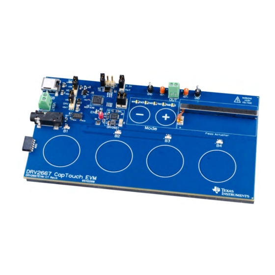
Decrement Mode Piezo Actuator External Power MSP430 Actuator ANALOG DRV2667 Analog In Programmer Connector Effect Buttons Press to play haptic effects. Figure 1. Board Diagram DRV2667 Evaluation Module SLOU323 – June 2013 Submit Documentation Feedback Copyright © 2013, Texas Instruments Incorporated... -
Page 5: Evaluation Module Operating Parameters
The DRV2667EVM-CT firmware contains sample haptic waveforms which showcase the features and benefits of the DRV2667. See the instructions below to power the board and begin using Demo mode. 1. Out of the box, the jumpers are set to begin demo mode using USB power. The default jumper settings... -
Page 6: Drv2667 Embedded Software
Figure 2. DRV2667EVM-CT Mode Sets Set Descriptions: 1. Demo Mode – contains a set of pre-designed effects that use the features of the DRV2667. This mode is great for demonstrating the DRV2667. 2. RAM Library Mode – a library created and stored in the RAM of the DRV2667. Library mode implements a RAM-based library of effects that are triggered by the MSP430 microcontroller. -
Page 7: Demo Mode
34.8 dB, 100 Vpp, Boost = 55 V 38.4 dB, 150 Vpp, Boost = 80 V 40.7 dB, 200 Vpp, Boost = 105 V SLOU323 – June 2013 DRV2667 Evaluation Module Submit Documentation Feedback Copyright © 2013, Texas Instruments Incorporated... -
Page 8: Demo Mode Descriptions
2.2.1 Mode Off – Alert Effects The effects in Mode Off are basic alert effects that use the DRV2667 waveform generator. The waveform generator reduces the demand of the host processor by creating the output waveform based on five parameters set in the DRV2667 register map. This eliminates the need for the host processor to output waveform samples continuously. -
Page 9: B3 - Alert 3
Alert 4 is a single waveform that produces a buzz. Figure 9. B4 – Alert 4 Figure 10. B4 – Alert 4 Continuous Repeat SLOU323 – June 2013 DRV2667 Evaluation Module Submit Documentation Feedback Copyright © 2013, Texas Instruments Incorporated... -
Page 10: B2 - Click And Release 1
The effect on button four is a ramp and release effect. When the button is pressed the waveform ramps up and when released it ramps down. Figure 13. Ramp and Release DRV2667 Evaluation Module SLOU323 – June 2013 Submit Documentation Feedback Copyright © 2013, Texas Instruments Incorporated... -
Page 11: B1 - Ramp Up
Button 4 – Pulse Button 4 consists of two waveforms a ramp up and ramp down. This produces a pulsating effect. Figure 16. B4 – Pulse SLOU323 – June 2013 DRV2667 Evaluation Module Submit Documentation Feedback Copyright © 2013, Texas Instruments Incorporated... -
Page 12: B1 - Sharp Click Using Fifo
Mode 2 – FIFO and RAM Effects The effects in Mode 2 are very similar to the previous modes; however, they do not use the DRV2667 waveform generator. Instead they use either the FIFO streaming mode or the internal RAM. The advantage of using FIFO or RAM is that the waveforms can be completely arbitrary. -
Page 13: B3 - Audio In
Figure 20 is an illustration of an audio signal producing vibration on the Piezo actuator. Figure 20. B3 – Audio In SLOU323 – June 2013 DRV2667 Evaluation Module Submit Documentation Feedback Copyright © 2013, Texas Instruments Incorporated... -
Page 14: Ram Library Mode
Alert 4 Design & Test Mode Design & Test contains modes that are used to design, test, and characterize the DRV2667. To access Design & Test modes use the following instructions: 1. Press and hold the increment mode button ("+") for approximately 3 seconds until the mode LEDs flash and the colored LEDs flash once. - Page 15 Device ID About the Board – the value appears on the mode LEDs in binary. About the Board Silicon revision LEDs: 11111 Code revision SLOU323 – June 2013 DRV2667 Evaluation Module Submit Documentation Feedback Copyright © 2013, Texas Instruments Incorporated...
-
Page 16: Return To Demo Mode
2. Release the button when the actuator buzzes and the mode LEDs flash. 3. Select from the Demo modes using the "+" and "–" buttons. DRV2667 Evaluation Module SLOU323 – June 2013 Submit Documentation Feedback Copyright © 2013, Texas Instruments Incorporated... -
Page 17: Hardware Configuration
Power Power Supply The DRV2667EVM-CT can be powered by USB or an external power supply (VBAT). Jumpers DRV and MSP are used to select the supply for the DRV2667 and the MSP430G2553, respectively. See the Table 7 for configuration options. -
Page 18: External Actuator
Figure 23. External I C Input The DRV2667 can be controlled by an external I2C source. To control externally, attach the external controller to the I2C header at the top of the board; be sure to connect SDA, SCL, and GND from the external source. -
Page 19: Analog/Pwm Input
Hardware Configuration www.ti.com There is also a special mode in the Design & Test set that allows you to save the DRV2667’s sequencer registers settings for playback at a later time. To store the sequencer: 1. Enter Design & Test Modes. Select Mode 0 – GUI Mode (00000’b) using the increment mode button (“+”). -
Page 20: Boost Voltage Programming Resistors
R1 and R2. To replace R1 and R2, first remove R3 and R4 and use Equation 3 to calculate the boost output voltage. DRV2667 Evaluation Module SLOU323 – June 2013 Submit Documentation Feedback Copyright © 2013, Texas Instruments Incorporated... - Page 21 Inductor selection plays a critical role in the performance of the DRV2667. The range of recommended inductor values is 3.3 μH to 22 μH. When a larger inductance is chosen, the DRV2667 boost converter automatically runs at a lower switching frequency and incurs less switching losses. The larger inductors;...
- Page 22 For example, when 50 V is applied to a 100-V rated capacitor, the capacitance will decrease by about 50%. Most capacitor vendors provide a capacitance versus voltage curve for reference. DRV2667 Evaluation Module SLOU323 – June 2013 Submit Documentation Feedback Copyright © 2013, Texas Instruments Incorporated...
-
Page 23: Msp430 Control And Firmware
Select the MSP430G2553 device • Copy the .h and .c files in the DRV2667EVM-CT project folder downloaded from ti.com into the new project directory SLOU323 – June 2013 DRV2667 Evaluation Module Submit Documentation Feedback Copyright © 2013, Texas Instruments Incorporated... - Page 24 MSP430 Control and Firmware www.ti.com MSP430 Actuator ANALOG DRV2667 EMULATION MSP-EXP430G2 Figure 26. DRV2667EVM-CT LaunchPad Connection DRV2667 Evaluation Module SLOU323 – June 2013 Submit Documentation Feedback Copyright © 2013, Texas Instruments Incorporated...
-
Page 25: Msp430 Pin-Out
GAIN1, feedback resistor control P2.6 GAIN0, feedback resistor control AVSS Analog ground DVSS Digital ground AVCC Analog supply DVCC Digital supply P1.0 Red LED SLOU323 – June 2013 DRV2667 Evaluation Module Submit Documentation Feedback Copyright © 2013, Texas Instruments Incorporated... -
Page 26: Schematic, Printed-Circuit Board Layouts, And Bill Of Materials
0.1ufd/100V PowerPad 0402 3.3uH/1.1A 1206 X7R VLS3010 Black Black +3.3V PowerPad 0.1ufd/25V 0603 GAIN0 0.1ufd/16V 0402 SC70-6 60V 115mA QFN32-RHB Figure 27. DRV2667EVM-CT Schematic DRV2667 Evaluation Module SLOU323 – June 2013 Submit Documentation Feedback Copyright © 2013, Texas Instruments Incorporated... -
Page 27: Pcb Layouts
PCB Layouts Figure 28 through Figure 32 are the PCB layouts for this EVM. Figure 28. DRV2667EVM-CT Top Silkscreen Figure 29. DRV2667EVM-CT Top Copper SLOU323 – June 2013 DRV2667 Evaluation Module Submit Documentation Feedback Copyright © 2013, Texas Instruments Incorporated... - Page 28 Schematic, Printed-Circuit Board Layouts, and Bill of Materials www.ti.com Figure 30. DRV2667EVM-CT Copper Layer 2 Figure 31. DRV2667EVM-CT Copper Layer 3 DRV2667 Evaluation Module SLOU323 – June 2013 Submit Documentation Feedback Copyright © 2013, Texas Instruments Incorporated...
- Page 29 Schematic, Printed-Circuit Board Layouts, and Bill of Materials www.ti.com Figure 32. DRV2667EVM-CT Bottom Copper Layer SLOU323 – June 2013 DRV2667 Evaluation Module Submit Documentation Feedback Copyright © 2013, Texas Instruments Incorporated...
-
Page 30: Bill Of Materials
RESISTOR,SMT,0402,THICK FILM,5%,1/16W,1.5K Panasonic ERJ-2RKF9761X RESISTOR SMD0402 THICK FILM 9.76K OHMS 1/10W 1% PANASONIC DIGI-KEY P9.76KLCT-ND ROHS ERJ-2RKF4991X RESISTOR SMD0402 4.99K 1%,1/16W ROHS PANASONIC DIGI-KEY P4.99KLCT-ND DRV2667 Evaluation Module SLOU323 – June 2013 Submit Documentation Feedback Copyright © 2013, Texas Instruments Incorporated... - Page 31 JACK USB MINIB SMT-RA 5PIN ROHS HIROSE DIGI-KEY H2959CT TP5000 VBST PC TESTPOINT, RED, ROHS KEYSTONE ELECTRONICS DIGI-KEY 5000K PHAT423535XX Actuator PIEZO Vibration Actuator Samsung Electro-Mechanics SLOU323 – June 2013 DRV2667 Evaluation Module Submit Documentation Feedback Copyright © 2013, Texas Instruments Incorporated...
- Page 32 Any exceptions to this are strictly prohibited and unauthorized by Texas Instruments unless user has obtained appropriate experimental/development licenses from local regulatory authorities, which is responsibility of user including its acceptable authorization.
- Page 33 FCC Interference Statement for Class B EVM devices This equipment has been tested and found to comply with the limits for a Class B digital device, pursuant to part 15 of the FCC Rules. These limits are designed to provide reasonable protection against harmful interference in a residential installation. This equipment generates, uses and can radiate radio frequency energy and, if not installed and used in accordance with the instructions, may cause harmful interference to radio communications.
- Page 34 Also, please do not transfer this product, unless you give the same notice above to the transferee. Please note that if you could not follow the instructions above, you will be subject to penalties of Radio Law of Japan. Texas Instruments Japan Limited (address) 24-1, Nishi-Shinjuku 6 chome, Shinjuku-ku, Tokyo, Japan http://www.tij.co.jp...
- Page 35 FDA Class III or similar classification, then you must specifically notify TI of such intent and enter into a separate Assurance and Indemnity Agreement. Mailing Address: Texas Instruments, Post Office Box 655303, Dallas, Texas 75265 Copyright © 2013, Texas Instruments Incorporated...
- Page 36 IMPORTANT NOTICE Texas Instruments Incorporated and its subsidiaries (TI) reserve the right to make corrections, enhancements, improvements and other changes to its semiconductor products and services per JESD46, latest issue, and to discontinue any product or service per JESD48, latest issue.
Need help?
Do you have a question about the DRV2667 and is the answer not in the manual?
Questions and answers