
Related Manuals for Anritsu 37 D Series


Summary of Contents for Anritsu 37 D Series
- Page 1 SERIES 37XXXD VECTOR NETWORK ANALYZER MAINTENANCE MANUAL P/N: 10410-00264 490 JARVIS DRIVE MORGAN HILL, CA 95037-2809 REVISION: C PRINTED: JULY 2007 COPYRIGHT 2007 ANRITSU CO.
- Page 2 WARRANTY The Anritsu product(s) listed on the title page is (are) warranted against defects in materials and workmanship for three years from the date of shipment. Anritsu’s obligation covers repairing or replacing products which prove to be defective during the warranty period.
- Page 5 Chapter 2—Replaceable Parts This chapter lists all replaceable subassemblies and components for all 37XXXD models. It explains the Anritsu exchange assembly program and provides parts ordering information. Chapter 3—Theory of Operation This chapter provides descriptions of the functional operation of the major assemblies contained in Se- ries 37XXXD Vector Network Analyzer systems.
- Page 6 Appendix C—Lightning 37000D Technical Data Sheet This appendix contains a copy of the 37000D Series Vector Network Analyzers, Technical Data Sheet, Anritsu part number 11410-00350. This datasheet provides performance specifications for all models in the series. Appendix D—ME7808B/C Broadband Measurement System Maintenance This appendix provides maintenance and verification instructions for the ME7808B/C Broadband Measurement System.
-
Page 7: Table Of Contents
Table of Contents Chapter 1 General Information SCOPE OF MANUAL · · · · · · · · · · · · · · · · · · · · · · · · · · · · · · · · · 1-3 INTRODUCTION ·... - Page 8 Table of Contents (Continued) Chapter 3 Theory of Operation INTRODUCTION · · · · · · · · · · · · · · · · · · · · · · · · · · · · · · · · · · · 3-3 SYSTEM OVERVIEW ·...
- Page 9 Table of Contents (Continued) LOG MAGNITUDE DYNAMIC ACCURACY TEST · · · · · · · · · · · · · · · · 4-15 Required Equipment ....... 4-15 Test Procedure .
- Page 10 Table of Contents (Continued) ERROR MESSAGES DURING MEASUREMENTS · · · · · · · · · · · · · · · · · 7-9 Lock Failure D or DE (60xx) ......7-9 Other Lock Failures .
- Page 11 Table of Contents (Continued) Appendix A Connector Care and Handling INTRODUCTION · · · · · · · · · · · · · · · · · · · · · · · · · · · · · · · · · · · A-3 PRECAUTIONS ·...
- Page 13 Chapter 1 General Information Table of Contents SCOPE OF MANUAL · · · · · · · · · · · · · · · · · · · · · · · · · · · · · · · · · 1-3 INTRODUCTION ·...
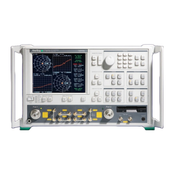
- Page 14 Figure 1-1. Series 37XXXD Vector Network Analyzer System 37XXXD MM...
-
Page 15: Scope Of Manual
All Anritsu instruments are assigned a six-digit ID number, such as IDENTIFICATION NUMBER “042503”. This number appears on a decal affixed to the rear panel. -
Page 16: System Description
SYSTEM DESCRIPTION GENERAL INFORMATION SYSTEM DESCRIPTION The 37XXXD Analyzers are microprocessor controlled Vector Network Analyzers. Each is a single-instrument system that contains a built-in signal source, a test set, and an analyzer subsystem. These analyzers are produced in eight models that cover a range of from 40 MHz to 65 GHz. -
Page 17: Standard Options
Failed assemblies are not field repairable. Once an assembly is found to be faulty, it should be returned to an authorized Anritsu Service Center for exchange. Refer to the description of the Exchange Assem- bly Program in Chapter 2, Replaceable Parts. -
Page 18: Internal Hardware Adjustments And Calibrations
NOTE A printed or disk file copy of the Service Log (with the failure in question) must be made available to Anritsu when ex- changing a failed assembly, or when requesting service sup- port. Refer to Chapter 2, Replaceable Parts, for further information. -
Page 19: System Test/Certification
Instruments with customer requested special modifications performed Modified Instruments by Anritsu will have an identifying Specials Modification number printed on the rear panel. This number will be preceded with the letters SM, that is, SM1234 is special modification number 1234. This manual contains information on servicing instruments fitted with SM5955 (67 GHz operation). -
Page 20: Service Software
The service software listed below is contained on the diskette located at the rear of this manual: Anritsu 37XXX Test Software (2300-178). This software contains a series of automated tests designed to insure the VNA signal paths are functioning properly and capable of support- ing stable calibrations and measurements. -
Page 21: Verification Kits
GENERAL INFORMATION SERVICE SUPPORT Verification Kits The Anritsu Verification Kits listed below are used in conjunction with the 37XXX Performance Verification Software. N Verification Kit (Model 3663) Contains precision N Connector components with characteristics that are traceable to the NIST. -
Page 22: Performance Specifications
37000D Technical Data Sheet. 1-11 SERVICE CENTERS Anritsu Company offers a full range of repair and calibration services at fully staffed and equipped service centers throughout the world. Ta- ble 2-1, located on page 2-2, lists all Anritsu services centers. - Page 23 GENERAL INFORMATION STATIC SENSITIVE COMPONENT HANDLING PROCEDURES Do not touch exposed contacts on Do not slide static sensitive com- Do not handle static sensitive com- any static sensitive component. ponent across any surface. ponents in areas where the floor or work surface covering is capable of generating a static charge.
-
Page 24: Recommended Test Equipment
Anritsu 3653 For instruments with Option 7S: Anritsu 3650-1* For instruments without Option 7: Anritsu 3652-1* For models 37X77D, 37X97D: Anritsu 3654B or Anritsu 3654C-1 For instruments with SM5955: Anritsu SC7556 Performance Verifica- Automates performance verification testing Anritsu 2300-496 tion Software... - Page 25 Oscilloscope None Tektronix, Inc. Model 2445 Power Meter 1, with: Power Range: –30 to +20 dBm Anritsu Model ML243xA Power A, O (1 mW to 100 mW) Meter Other: GPIB controllable Power Sensor 1 Frequency Range: Useable to the full fre-...
- Page 27 Chapter 2 Replaceable Parts Table of Contents INTRODUCTION · · · · · · · · · · · · · · · · · · · · · · · · · · · · · · · · · · · 2-3 EXCHANGE ASSEMBLY PROGRAM ·...
- Page 28 WaiGaoQiao Free Trade Zone Pudong, Shanghai 200131, P.R. China Telephone: 21-5868-0226 FAX: 21-5868-0588 For the latest service and sales information in your area, please visit: http://www.us.Anritsu.com/contacts/default.aspx?lc=Eng&cc=US&rc=ARO and choose a country for regional contact information. Anritsu Part Number: 00986-00211, updated July 31, 2007...
-
Page 29: Introduction
PROGRAM blies. If a malfunction occurs in one of these subassemblies, the defec- tive item can be exchanged. Upon receiving your request, Anritsu will ship the exchange subassembly to you, typically within 24 hours. You then have 45 days in which to return the defective item. All exchange... -
Page 30: Replaceable Subassemblies And Parts
All parts listed in Tables 2-2 through 2- 4 may be ordered from your lo- INFORMATION cal Anritsu service center (Table 2-1, page 2-2). Or, they may be or- dered directly from the factory at the following address: Anritsu Company... - Page 31 REPLACEABLE PARTS PARTS ORDERING INFORMATION Table 2-2. Printed Circuit Board Assemblies Reference Original Replacement Assembly / Part Designator Part Number Part Number First Local Oscillator 57661-3 ND60314 Second Local Oscillator 61835-3 61835-3 A3/A6 Test A, Test B IF Processor D38503-3 D38503-3 Reference IF Processor D41794-5...
- Page 32 PARTS ORDERING INFORMATION REPLACEABLE PARTS Table 2-3. RF Source and Test Set Assembly RF/Microwave Components Assembly / Part Description Original Part Number Replacement Part Number YIG Oscillator (all models) C21620-1 C21620-1 Switched Filter (all models) D45244 D45244 Source Down Conversion Module (all models) D27532 D27532 Coupler (20 and 40 GHz models)
- Page 33 REPLACEABLE PARTS PARTS ORDERING INFORMATION Table 2-4. Miscellaneous Replaceable Subassemblies and Parts* Assembly / Part Description Replacement Part Number Floppy Disk Drive 2000-1364 ND54935 Power Supply ND63006 LCD display 15-100 Backlight Driver PCB for LCD 2000-1365 Basic Measurement Software (“BMS”, 2 disk set) 2300-500 Backup battery for A9 PCB Purchase Locally...
- Page 34 PARTS ORDERING INFORMATION REPLACEABLE PARTS Printed Circuit Board Assemblies, A13 to A16 Fan Assembly Power Supply Module Printed Circuit Board Assemblies, A1 to A9 Signal Source Module Front Panel Assembly (Includes Front Panel PCB) Figure 2-1. Major Assemblies Location Diagram (Top View) 37XXXD MM...
- Page 35 REPLACEABLE PARTS PARTS ORDERING INFORMATION Figure 2-2. Signal Source Parts Location Diagram 37XXXD MM 2-9/2-10...
- Page 37 Chapter 3 Theory of Operation Table of Contents INTRODUCTION · · · · · · · · · · · · · · · · · · · · · · · · · · · · · · · · · · · 3-3 SYSTEM OVERVIEW ·...
-
Page 39: Introduction
Chapter 3 Theory of Operation INTRODUCTION This chapter provides a brief overview of the functional assemblies and major parts that comprise a typical 37XXXD VNA system. It also briefly describes the operation of each major assembly. Further details of the ME7808B/C Broadband system are found in Appendix D. SYSTEM OVERVIEW 37XXXD Vector Network Analyzers are ratio measurement systems used to measure complex vector signal characteristics (real/imaginary,... -
Page 40: System Overview
SYSTEM OVERVIEW THEORY OF OPERATION An internal service log stores a record of system failures, data about the failures, and other key system service information. The service log is implemented using internal battery-backed SRAM memory. 37XXXD MM... - Page 41 THEORY OF OPERATION SYSTEM OVERVIEW TEST SET MODULE* EXTERNAL PORT 1 KEYBOARD QUAD IF / SYNC/ DET µP FLTR / S/H / A/D SAMPLER/BUFFER MAIN PROCESSOR PCB LOCK REAR YIG OSC µP FRONT PANEL PANEL BBRAM 2-20 GHz 68030 GRAPHICS LCD DISPLAY PROCESSOR TRANSFER...
- Page 42 SYSTEM OVERVIEW THEORY OF OPERATION Port Test B Test B Port 1 Front Panel Port 1 Step RF Cable Bias Front coupler Panel Control Lines from A8 PCB Cable Test A Front Port 2 Source Port 2 Panel RF Bias Tee Switched Doubler Coupler...
- Page 43 THEORY OF OPERATION SYSTEM OVERVIEW Control from A8 PCB 10 MHz 10 MHz A7 PCB Control from A8 PCB Ref A Front Panel RF 40 MHz to Source Cable (2) Ref A Switched 20 GHz Doubler Transfer Osc. Filter 40 MHz to 40 GHz Module Switch 40 MHz to...
- Page 44 SYSTEM OVERVIEW THEORY OF OPERATION Control from A8 PCB 16.8 GHz Source Low Pass Test B Quadrupler 37 GHz Filter 9.5 to Test B (1) Module Hi Pass Filter 16.25 GHz 38 to 65 GHz (SQM) SPDT Switch Port 1 MUX Test B 40 MHz to 65 GHz (1) Front Coupler...
- Page 45 THEORY OF OPERATION SYSTEM OVERVIEW Control from A8 PCB First LO Second LO 16.8 GHz (A1 PCB) (A2 PCB) Source Ref A Ref A Lowpass (357 to 536 MHz) (25 to 272 MHz) Quadrupler 37 GHz 38 to 65 GHz 38 to 65 GHz filter 9.5 to...
-
Page 46: Analog Subsystem Assemblies
ANALOG SUBSYSTEM ASSEMBLIES THEORY OF OPERATION ANALOG SUBSYSTEM The following sections briefly describe the major assemblies that com- ASSEMBLIES prise the VNA Analog Subsystem. Descriptions of the functions per- formed by each assembly are also included. Signal Source Module The Signal Source Module consists of the items listed below; refer to the block diagram of the Analog Subsystem (Figure 3-3). -
Page 47: Test Set Module, 20 Ghz And 40 Ghz Instruments
THEORY OF OPERATION ANALOG SUBSYSTEM ASSEMBLIES The system A9 Main Microprocessor PCB sends the data that repre- sents the desired operating frequency to the A21A2 (Source Control) PCB, which converts the frequency data to analog signals. These sig- nals are then sent to the A21A1 YIG/Bias Controller PCB. This PCB converts the analog signals to YIG main tuning coil current. - Page 48 ANALOG SUBSYSTEM ASSEMBLIES THEORY OF OPERATION In 20 GHz models, RF from the Source Module is routed to the Trans- fer Switch. In 40 GHz models, RF from the Source Module is routed into the Source Doubler Module (SDM) and, if the instrument sweep is set to any frequency above 20.0 GHz, the frequency is doubled.
-
Page 49: Test Set Module, 50 Ghz And 65 Ghz Instruments
THEORY OF OPERATION ANALOG SUBSYSTEM ASSEMBLIES Both Reference signals and both Test Signals are routed into the Sam- pler/Down Conversion Modules for down conversion to 2.5 MHz (3rd IF signal). This down conversion is accomplished by using LO1 and LO2 found on the A1 and A2 PCBs. Before use by the Sam- pler/Down Conversion Module, the signal from LO1 is amplified by the Power Amplifier assembly (mounted on the Sampler/Down Conversion Module) for a power gain of about 30 dB. - Page 50 ANALOG SUBSYSTEM ASSEMBLIES THEORY OF OPERATION When operating below 38 GHz, signals pass through the SDM (through the pass-through or doubling sections) and are routed to the Transfer Switch (a different model switch than is used in the 20 GHz and 40 GHz instruments).
-
Page 51: A7 Pcb 10 Mhz Timebase
THEORY OF OPERATION ANALOG SUBSYSTEM ASSEMBLIES A7 PCB The 10 MHz system clock is based on an OCXO mounted on the A7 PCB. The A7 PCB also contains a fixed 2.42 MHz Local Oscillator and 10 MHz Timebase an 80 kHz calibration signal. The 80 kHz calibration signal is periodi- cally sent to the A3, A4, and A6 PCBs for self-calibration of IF ampli- fier circuits. -
Page 52: Receiver Module
ANALOG SUBSYSTEM ASSEMBLIES THEORY OF OPERATION Receiver Module The Receiver Module consists of the items listed below (refer to Fig- ure 3-3): Quad Sampler/Down Conversion Module with integrated SRD (step recovery diode) Power Amplifier A1, LO1 PCB A2, LO2 PCB The Receiver Module is based on a four channel, two stage Sampler/Down Conversion module that converts the 40 MHz to 65 GHz signals to 2.5 MHz signals. - Page 53 THEORY OF OPERATION ANALOG SUBSYSTEM ASSEMBLIES MICROPROCESSOR A18 REAR DRAM SRAM BATTERY A15 GRAPHICS PCB PANEL PCB MEMORY MEMORY BACKED ARRAY ARRAY WITH RAM/CLOCK REAR PANEL BATTERY BIAS TEE BIAS TEE IN EPROM / GRAPHICS INTERRUPT DRAM P / B FLASH PROCESSOR VECTOR...
-
Page 54: A8, Source Lock/Signal Separation And Control Pcb
ANALOG SUBSYSTEM ASSEMBLIES THEORY OF OPERATION A8, Source The Source Lock Phase Comparator circuit on the A8 Source Lock/ Lock/Signal Signal Separation Control PCB compares the Source Lock (Reference Separation and A/B) signal from the Receiver Module with a signal derived from the 10 MHz reference oscillator. -
Page 55: A7 Pcb, Lo3
THEORY OF OPERATION ANALOG SUBSYSTEM ASSEMBLIES A7 PCB, LO3 The A7, Third Local Oscillator (LO3) Assembly, provides a fixed 10 MHz Reference Timebase and a 2.42 MHz Local Oscillator signal that is used on the A3, A4, and A6 PCBs to down-convert the 2.5 MHz IF signals to 80 kHz. -
Page 56: Digital Subsystem Assemblies
DIGITAL SUBSYSTEM ASSEMBLIES THEORY OF OPERATION DIGITAL SUBSYSTEM The following sections briefly describe the major assemblies that com- ASSEMBLIES prise the VNA Digital Subsystem. The digital subsystem provides all system control, I/O interface, digital signal processing, and data pre- sentation functions. The major assemblies that comprise the VNA digi- tal PCB subsystem are listed below (refer to Figure 3-4): A9, Main Processor PCB A13, I/O Interface #1 PCB... -
Page 57: A13 I/O Interface #1 Pcb Assembly
THEORY OF OPERATION DIGITAL SUBSYSTEM ASSEMBLIES System boot-up EPROM—This chip contains the boot-up instruc- tions used by the system CPU at power-up. A13 I/O Interface #1 This PCB assembly performs the following functions: PCB Assembly Floppy drive control—interface for the Floppy Drive Assembly External Keyboard control—interface for the front panel Keyboard connector Interface for the A18 Rear Panel PCB Assembly (below) -
Page 58: A15 Graphics Processor Pcb Assembly
MAIN CHASSIS ASSEMBLIES THEORY OF OPERATION A15 Graphics This PCB assembly contains circuitry that simultaneously drives both Processor PCB the LCD display and an external VGA monitor (if used) as follows: Assembly Receives measurement and display information from the A9 Main Processor PCB and generates screen display (video) infor- mation. -
Page 59: Front Panel Assembly
THEORY OF OPERATION MAIN CHASSIS ASSEMBLIES Front Panel Assembly The Front Panel Assembly consists of the following assemblies and parts: A19 Front Panel Switch PCB—this assembly contains all of the front panel switches for the VNA. A20 Front Panel Control PCB—this assembly contains the de- code logic for the switches located on the A19 Front Panel Switch PCB. -
Page 60: Power Supply Module
MAIN CHASSIS ASSEMBLIES THEORY OF OPERATION Power Supply Module The Power Supply Module is a single self contained assembly mounted on the left side wall of the chassis, behind the LCD. This module pro- vides: Unregulated +5, +9, ±18, and ±27 Vdc supply voltages to the other assemblies of the 37XXXD Thermal and over-current shutdown protection circuitry Sensing and input power regulation for operation with... - Page 61 Chapter 4 Operational Performance Tests Table of Contents INTRODUCTION · · · · · · · · · · · · · · · · · · · · · · · · · · · · · · · · · · · 4-3 CHECKING THE SERVICE LOG ·...
-
Page 63: Introduction
Chapter 4 Operational Performance Tests INTRODUCTION The tests in this chapter provide a means of fully testing the 37XXXD VNA system for proper operation and signal stability. These tests are intended to be used as a periodic check of the operational functionality of the VNA. -
Page 64: Checking The Service Log
CHECKING THE SERVICE LOG OPERATIONAL TESTS CHECKING THE SERVICE Checking the service log consists of viewing the entries written into the log. CAUTION The service log contains historical information about instru- ment condition and any failures that may have occurred. It should be cleared only by a qualified service engineer. -
Page 65: Self Test
OPERATIONAL TESTS SELF TEST SELF TEST The self test performs a series of tests that verify that various internal VNA circuits are functional and operating properly. To start the self test: Step 1. Press the Option Menu key (Enhancement key group) to dis- play the OPTIONS menu. -
Page 66: Performance Tests
Specifications that are typical are identical to factory specifications for new instruments. Anritsu does not guarantee the VNA will meet these specifications. If a test fails by a small margin, this does not indicate a problem with the instrument. -
Page 67: Required Equipment
High quality RF cable suitable for the frequency range of the in- strument. Anritsu 3670 or 3671 series throughlines are strongly recommended. High quality female to female adapter, such as Anritsu part num- ber 33KFKF50B. Necessary if the above cable does not have a fe- male connector on both ends. - Page 68 PERFORMANCE TESTS OPERATIONAL TESTS From your Windows-based PC, run the program (3700Test.exe). The program’s interface will appear similar to the display below: Figure 4-1. 2300-178 Software Interface Connect the GPIB cable between the PC and the upper GPIB connec- tor of the VNA rear panel (labeled IEEE 488.2 GPIB). Turn on the VNA and verify the instrument address is 6 (found under the Utility Menu Key |GPIB ADDRESSES).
-
Page 69: Running The Tests
If the test fails, performing a Source Lock Threshold calibration may solve the problem. If this does not solve the problem, it must be cor- rected by a trained Anritsu Service Engineer. Source and LO Tests: These tests use built-in VNA diagnostics to check all phase lock loop error voltages of the RF source, LO1, and LO2 of the down conversion section. - Page 70 Test Ports is of good quality and all external ca- bles are connected properly. If this does not solve the problem, it must be corrected by a trained Anritsu Service Engineer. Non-Ratio Stability: This test checks the general stabilty of the Non-Ratio channels. Raw data is displayed, stored to memory, then divided by itself resulting in a very smooth RF display at high resolution.
- Page 71 If the test fails, the results may be improved by performing a Port 1 ALC calibration. If this solves the problem, a Port 2 ALC calibration and Source Lock Threshold Calibrations should also be performed. If the test continues to fail, it must be corrected by a trained Anritsu Service Engineer. 37XXXD MM...
- Page 72 (see Additoinal Required Equipment at the beginning of this section). A precision 10 MHz ref- erence signal (such as that found on an Anritsu MG369XA series synthesizer) should be connected to the rear panel of the counter. Do not use the 37XXXD 10 MHz OUT as a reference for the counter.
- Page 73 Ensure that no RF cables are attached during the test. The assur- ance airline and offset short are typically available only from Anritsu Service Centers. The test program will use the ripple extrac- tion technique to derive the corrected directivity of both Test Ports.
- Page 74 (in the view of the user) or successful to attempt a repair. If several errors appear in one day, a significant problem exists and a repair should be performed by an Anritsu Service Engi- neer. 4-14...
-
Page 75: Log Magnitude Dynamic Accuracy Test
0 dBm. An external step attenuator TEST that has been accurately characterized at the Anritsu Calibration Lab is used. S21 only measurements at 2.0 GHz will be performed manu- ally at each step of the attenuator. Uncertainty associated with the step attenuator and characteristic VNA uncertainty are part of the cri- teria used in the Pass or Fail determination for each attenuation step. -
Page 76: Test Procedure
LOG MAGNITUDE DYNAMIC ACCURACY TEST OPERATIONAL TESTS Test Procedure WARNING Incorrectly installing the step attenuator into the driver fix- ture will damage the step attenuator. Carefully follow the di- rections specified below: Step 1. Default the VNA. Step 2. Install a test cable to both Port 1 and Port 2 (with V-to-K adapters on the cables if the VNA has V connector test ports). - Page 77 OPERATIONAL TESTS LOG MAGNITUDE DYNAMIC ACCURACY TEST Step 8. Complete the calibration using default settings for other devices. WARNING Incorrectly installing the step attenuator into the driver fix- ture will damage the step attenuator. Read the following step carefully. Step 9. Observe the white dots and/or beveled connector corners that designate Pin 1 on the driver fixture and the attenu- ator ribbon cable plug, then plug the ribbon cable into the...
-
Page 78: Analysis Of The Measurement
LOG MAGNITUDE DYNAMIC ACCURACY TEST OPERATIONAL TESTS Analysis of the A visual estimate of the average value of the data points is sufficient Measurement for the purposes of this test. Record the (visual) average value for each attenuation step in Column B of Table 4-1 (page 4-19). Open the data file (using a text reader program) on the Characteriza- tion Disk of the step attenuator. - Page 79 OPERATIONAL TESTS LOG MAGNITUDE DYNAMIC ACCURACY TEST Figure 4-2. Log Magnitude/Dynamic Accuracy Test Result 37XXXD Log Magnitude Dynamic Accuracy Test Model:______________________ Serial Number:____________________ Date:________ Operator:____________________ Step Atten. ID:_____________________ --C-- --A-- Attenuation --B-- --D-- --E-- --F-- Attenuation Device Measured Composite Col. C + Col. D Col.
- Page 81 Chapter 5 System Performance Verification Table of Contents INTRODUCTION · · · · · · · · · · · · · · · · · · · · · · · · · · · · · · · · · · · 5-3 CALIBRATION AND MEASUREMENT CONDITIONS ·...
-
Page 83: Introduction
Chapter 5 System Performance Verification INTRODUCTION This chapter provides specific procedures to be used to verify that the VNA is making accurate, traceable S-parameter measurements. The operational performance tests described in Chapter 4 should be per- formed at least once anually, and prior to verifying the system perfor- mance test procedures in this chapter. -
Page 84: Special Precautions
MEASUREMENT ACCURACY PERFORMANCE VERIFICATION Special Precautions When performing the procedures in this chapter, observe the following precautions: Minimize vibration and movement of the system, attached compo- nents, and through-cable. Clean and check the pin depth and condition of all adapters, through-cable(s), and calibration components. -
Page 85: Verification Result Determination
Factory Standard 37XXX Vector Net- work Analyzer System (at Anritsu). The factory Standard 37XXX system is traceable to NIST through the Anritsu Calibration Labora- tory’s Impedance Standards. These standards are traceable to NIST through precision mechanical measurements, NIST approved micro- wave theory impedance derivation methods, and electrical impedance comparison measurements. -
Page 86: Verification Procedure
Kit for the connector type in use; refer to Table 1-1) External computer/controller; refer to Table 1-1 Anritsu Calibration Kit identical to the Test Port connectors of the VNA; refer to Table 1-1 Anritsu Verification Kit identical to the Test Port connectors of the VNA;... -
Page 87: Vna Traceability
PERFORMANCE VERIFICATION VNA TRACEABILITY VNA TRACEABILITY According to the International Vocabulary of Basic and General Terms in Metrology (VIM), BIPM, IEC, IFCC, ISO, IUPAC, IUPAP, OIML, 2nd ed., 1993, definition 6.10, traceability is defined as the property of the result of a measurement or the value of a standard that can be related to stated references through an unbroken chain of comparisons all hav- ing stated uncertainties. - Page 88 The horizontal path shows the conventional traceability chain for the verification kit. The stated uncertainty in the verification program co- mes from three major sources: NIST Report Anritsu Reference Standards Device-under-test NIST Airline Assurance Airline (i.e., Beadless Airline) (i.e., Partially Supported...
- Page 89 Chapter 6 Adjustments Table of Contents INTRODUCTION · · · · · · · · · · · · · · · · · · · · · · · · · · · · · · · · · · · 6-3 LO1 CALIBRATION ·...
-
Page 91: Introduction
Chapter 6 Adjustments INTRODUCTION This chapter contains procedures that are used to restore the calibra- tion of the VNA signal source and the related source lock system as- semblies. Use these procedures after various signal source related as- semblies have been replaced due to troubleshooting or repair activities. -
Page 92: Lo1 Calibration
LO1 CALIBRATION ADJUSTMENTS Post Calibration After the calibration process is completed, perform the following ac- Actions tions, as appropriate: If calibration passes: Save the calibration data to (hard) disk, as follows: Step 1. Press the Option Menu key (Enhancement key group) to dis- play the OPTIONS menu. -
Page 93: Lo2 Calibration
ADJUSTMENTS LO2 CALIBRATION LO2 CALIBRATION This procedure uses the VNA’s internal diagnostics and calibration menus to adjust the A2 second LO PCB assembly. Perform this calibation procedure if: The A2 PCB is replaced. Display of DIAGNOSTICS/TROUBLESHOOTING/LO2 MAIN PHASELOCK VOLTAGE is outside of the limit lines. Calibration Perform the following steps: Procedure... - Page 94 LO2 CALIBRATION ADJUSTMENTS Post Calibration After the calibration process is completed, perform the following ac- Actions tions, as appropriate: If the calibration passes: Save the calibration data to (hard) disk, as follows: Step 1. Press the Option Menu key (Enhancement key group) to dis- play the OPTIONS menu.
-
Page 95: Frequency Calibration
Procedure Equipment Required: Refer to Table 1-1 for further information about the following equip- ment: Anritsu MF241XB Frequency Counter or equivalent EIP brand counter equipped with Band 3 Input and GPIB capability RF/Microwave Cable GPIB cable (Anritsu 2100-2, or equivalent) - Page 96 FREQUENCY CALIBRATION ADJUSTMENTS Procedure: Step 1. Press the Option Menu key (Enhancement key group) to dis- play the OPTIONS menu. Step 2. Select DIAGNOSTICS from the menu, then select in se- quence: H/W CALIBRATION | SOURCE FREQUENCY CALIBRATION (below). DIAGNOSTICS OPTIONS HARDWARE CALIBRATIONS...
- Page 97 ADJUSTMENTS FREQUENCY CALIBRATION Post Calibration After the calibration process is completed, perform the following ac- tions, as appropriate: Actions If calibration passes: Save the calibration data to (hard) disk, as follows: Step 1. Press the Option Menu key (Enhancement key group) to dis- play the OPTIONS menu.
-
Page 98: Rf Power/Alc Calibration
RF POWER/ALC CALIBRATION ADJUSTMENTS RF POWER/ALC This procedure uses the VNA’s internal diagnostics and calibration CALIBRATION menus, in conjunction with a suitable power meter, to adjust the out- put power level of the signal source throughout the range of the VNA model being calibrated. - Page 99 Equipment Required: Refer to Table 1-1 for further information about the following equip- ment: Anritsu ML24XXA with Version 2.02 or later, with Anritsu Power Sensors MA2474A (use sensor SC6230 for 50 and 65 GHz mod- els) GPIB cable (Anritsu 2100-2, or equivalent)
- Page 100 Follow the directions displayed on the screen to set-up and connect the power meter to the VNA. Refer also to Figure 6-2. Select START ALC CALIBRATION from the menu. Dedicated GPIB ANRITSU 37XXXD ANRITSU ML24XXA Power Meter Power Sensor Figure 6-2.
- Page 101 ADJUSTMENTS RF POWER/ALC CALIBRATION Post Calibration After the calibration process is completed, perform the following ac- tions, as appropriate: Actions If calibration passes: Save the calibration data to (hard) disk, as follows: Step 1. Press the Option Menu key (Enhancement key group) to dis- play the OPTIONS menu.
-
Page 102: Source Lock Threshold
SOURCE LOCK THRESHOLD ADJUSTMENTS SOURCE LOCK This procedure uses the VNA internal diagnostics and calibration THRESHOLD menus to adjust the source lock threshold of the phase-lock loop. Per- form this calibation procedure: If the Low Power Phase Lock Test (Chapter 4) fails. Anytime the Port 1 ALC Calibration is done. - Page 103 ADJUSTMENTS SOURCE LOCK THRESHOLD Post Calibration After the calibration process is completed, perform the following ac- tions, as appropriate: Actions If calibration passes: Save the calibration data to (hard) disk, as follows: Step 1. Press the Option Menu key (Enhancement key group) to dis- play the OPTIONS menu.
- Page 105 Chapter 7 Troubleshooting Table of Contents INTRODUCTION · · · · · · · · · · · · · · · · · · · · · · · · · · · · · · · · · · · 7-3 POWER-UP PROBLEMS ·...
- Page 106 Many of the troubleshooting procedures presented in this chapter require the removal of instrument covers to gain access to printed circuit assemblies and other major assemblies. WARNING Hazardous voltages are present inside the instrument when ac line power is connected. Turn off the instrument and remove the line cord before removing any covers or panels.
-
Page 107: Introduction
Insufficient care or train- ing will often result in damage to the instrument and cause increased expense and down time. Note that every Anritsu Service Center has factory-trained Service Engineers who can solve all 37XXXD operation problems quickly and reliably, often with warranted repairs. -
Page 108: Power-Up Problems
POWER-UP PROBLEMS TROUBLESHOOTING Step 1. Remove the bottom cover as described in Section 8-3. Step 2. Check the power supply voltages at J4 and J13 of the motherboard. The correct voltages and acceptable AC rip- ple are listed below: Table 7-1. DC Power Supply Voltage Checks Connect To: 372XXA A17 Motherboard... -
Page 109: Hard/Floppy Disk And Display Problems
A software utility to archive saved 37XXXD files on a PC is available on the Anritsu VNA Software Util- ities CD (Anritsu part number 2300-481). Step 1. -
Page 110: Other Boot-Up Problems
OTHER BOOT-UP PROBLEMS TROUBLESHOOTING OTHER BOOT-UP As the VNA boots, communication with several subsystems is at- PROBLEMS tempted. If the process stops before boot-up is complete, the last item displayed on the LCD is typically the failing assembly. For example, if the instrument does not boot-up beyond the “Initializing GPIB (A13/A18)”... -
Page 111: Understanding The Service Log
37XXXD. Numerical data with no easily understood identifying labels is of use only to Anritsu Service personnel in the process of PC board repair. PCB repair is a factory-only function. The following items of information found in the Service Log are highly... -
Page 112: Diagnostic Displays
DIAGNOSTIC DISPLAYS TROUBLESHOOTING SWP=R or SWP=F This indicates whether the instrument was in forward or reverse sweep when the problem occurred, and is useful in Phase Lock Failure troubleshooting and RF Unleveled problems. PWR –x.x All 37XXXD instruments have default power settings of –7 dBm or above shown under the Setup Menu / Test Signals key sequence. -
Page 113: Error Messages During Measurements
Chapter 6. If the condi- tion persists, the difficult nature of this problem means that the 37XXXD should be returned to an Anritsu Service Center where fac- tory-trained Service Engineers and replacement parts are available. - Page 114 ALC Calibrations (Chapter 6) may solve the problem. If the problem persists, the difficult nature of this problem means the best solution is to return the VNA to an Anritsu Service Center for repair. IF Cal Failures (during self-test or measurement) If only “Test A”...
-
Page 115: Measurement Accuracy Problems
TROUBLESHOOTING MEASUREMENT ACCURACY PROBLEMS MEASUREMENT ACCURACY PROBLEMS All Data on All Refer to the block diagrams in Chapter 3 that are labeled "Signal Channels is Greatly Paths.” Inaccurate For 50 and 65 GHz models, refer to the block diagram of the Test Sig- nal paths (Figure 7-4). - Page 116 NON-RESPONSE OR OTHER UNUSUAL BEHAVIOR TROUBLESHOOTING Figure 7-2. Error Code DE Lock Failure Troubleshooting (50 and 65 GHz models only) (1 of 3) 7-12 37XXXD MM...
- Page 117 TROUBLESHOOTING NON-RESPONSE OR OTHER UNUSUAL BEHAVIOR Go to Fails in Forward only ? Fails below 38 GHz? Fails above 38 Fails above 38 GHz? GHz? not logical Normal power at Normal power at Normal power at Port 1 (S21)? Port 1(S21)? Port 1(S21)? transfer sw or A8 Ref A MUX coupler...
- Page 118 NON-RESPONSE OR OTHER UNUSUAL BEHAVIOR TROUBLESHOOTING Fails Reverse not logical only? Fails below 38 GHz? Fails above 38 Fails above 38 GHz? GHz? not logical Normal power at Normal power at Normal power at Port 2 (S12)? Port 2 (S12)? Port 2 (S12)? A8, transfer sw Ref B MUX failure...
- Page 119 TROUBLESHOOTING NON-RESPONSE OR OTHER UNUSUAL BEHAVIOR Lock Failure DE (error code 6XXX) Verify Front Panel RF cables (Opt.15 only) are connected correctly Fails both Forward and Fails Forward Fails Reverse Reverse? only? only? Normal power at Normal power at Normal power at Port 1? Port 1 (S21) ? Port 2 (S12)?
- Page 120 NON-RESPONSE OR OTHER UNUSUAL BEHAVIOR TROUBLESHOOTING Table 7-2. Typical Reference Signal Values in dBm (50 and 65 GHz models only) Sampler/Down Frequency SQM In SDM Out MUX J4 MUX J1 Conversion Module Input 20 GHz –26 37 GHz –28 40 GHz –28 50 GHz –23...
- Page 121 Chapter 8 Removal and Replacement Procedures Table of Contents INTRODUCTION · · · · · · · · · · · · · · · · · · · · · · · · · · · · · · · · · · · 8-3 EQUIPMENT REQUIRED ·...
-
Page 123: Introduction
EQUIPMENT REQUIRED All procedures in this chapter require the use of either a #1 or #2 size Phillips type screw driver. Most procedures require the use of a 5/16 inch wrench and the Anritsu 01-201 (8 inch/pounds) Torque Wrench. 37XXXD MM... -
Page 124: Covers
COVERS REMOVE AND REPLACE COVERS Adjustment and troubleshooting operations require removal of the top cover. Replacement of some VNA assemblies and parts require re- moval of all covers. The following procedures describe this process. NOTE It is only necessary to loosen the VNA handle assemblies to remove the top, bottom, or side covers. - Page 125 REMOVE AND REPLACE COVERS CAUTION The green headed screws have Metric threads. Step 2. To remove the top cover: n Place the VNA in normal (top-side up) position. n Remove the feet from the two top corners at the rear of the VNA (Figure 8-1).
-
Page 126: A1 To A16 Pcbs
A1 TO A16 PCBS REMOVE AND REPLACE A1 TO A16 PCBS This section provides instructions for removing and replacing the A1 through A9 and A13 through A16 PCBs, which are located underneath the covers of the large and small card-cages, respectively. Preliminary: q Switch the VNA power to off. -
Page 127: A1 To A16 Pcbs
REMOVE AND REPLACE A1 TO A16 PCBS A9 PCB Assembly PCB Assemblies A13-A16 Printed Circuit Board Assemblies, A1-A8 Figure 8-2. A1 to A16 PCB Assemblies Removal Diagram 37XXXD MM... -
Page 128: A24 Vme Bus Terminator Pcb
A24 VME BUS TERMINATOR PCB REMOVE AND REPLACE A24 VME BUS This section provides instructions for removing and replacing the A24 TERMINATOR PCB VME Bus Terminator PCB assembly. Preliminary: q Switch VNA power off. Remove the power cord. q Remove bottom cover (Section 8-3). Remove/Replace Procedure: Step 1. -
Page 129: Front Panel Assembly
On instruments with Option 15V (found only on 50 and 65 GHz instruments), there is a very high risk of damage to RF cables and connectors during re-assembly. Such instru- ments should be returned to an Anritsu Service Center for repairs to the front panel assembly. Remove/Replace Procedure: Step 1. - Page 130 FRONT PANEL ASSEMBLY REMOVE AND REPLACE Step 2. Remove the four corner screws and the top center screw that secure the front panel assembly to the chassis (see Figure 8-5). Figure 8-5. Removal of Front Panel Assembly Step 3. Place the VNA on its top (bottom-side up). Step 4.
- Page 131 REMOVE AND REPLACE FRONT PANEL ASSEMBLY Step 9. On 300 series models, disconnect the cables from the front panel Bias Input BNC connectors to connector P2 on the A18 Rear Panel PCB at A18, P2 end. (A18, P2 is the con- nector nearest to the bottom lip of the rear panel.) Step 10.
-
Page 132: Liquid Crystal Display (Lcd)
LCD will likely solve display problems. CAUTION Due to the likelihood of damage to RF cables and connectors, Anritsu advises to NOT remove the front panel of 50 and 65 GHz instruments having Option 15V to perform this re- pair. Preliminary: q Switch the VNA power to off and remove the power cord. -
Page 133: Rear Panel Assembly
REMOVE AND REPLACE REAR PANEL ASSEMBLY REAR PANEL ASSEMBLY This section provides instructions for removing and replacing the Rear Panel Assembly. Equipment Required: Phillips Screwdriver (#2) Open-end Wrenches (various sizes) Preliminary: q Switch the VNA power to off and remove the power cord. q Remove all covers (Section 8-3). - Page 134 REAR PANEL ASSEMBLY REMOVE AND REPLACE Remove/Replace Procedure: Step 1. Disconnect all cables which are connected to the rear panel and to the A18 rear panel PCB. Figure 8-6. Rear Panel Mounting Screws Step 2. Remove the three screws on each side of the chassis that fasten to the rear panel assembly.
-
Page 135: Fan Assembly
REMOVE AND REPLACE FAN ASSEMBLY 8-10 FAN ASSEMBLY This section provides instructions for removing and replacing the Rear Panel Fan Assembly. Preliminary: q Switch the VNA power to off and remove the power cord. q Remove all covers (Section 8-3). q Remove the Rear Panel (Section 8-9). -
Page 136: Power Supply Module
POWER SUPPLY MODULE REMOVE AND REPLACE 8-11 POWER SUPPLY This section describes removing and replacing the Power Supply mod- MODULE ule that is mounted on the frame of the instrument behind the LCD. Power Supply Removal: DANGER Failure to remove the power cord before beginning this oper- ation can result in a fatal electric shock. -
Page 137: A18 Rear Panel Pcb
REMOVE AND REPLACE A18 REAR PANEL PCB 8-12 A18 REAR PANEL PCB This section provides instructions for removing and replacing the A18 Rear Panel PCB assembly. Equipment Required: q Nut Driver, inch q Nut Driver, inch q Phillips Screwdriver (#2) Preliminary: q Switch the VNA power to off and remove the power cord. -
Page 138: Test Set Module Assemblies
RF cabling, Phillips-head screws, and unplugging bias cables. Replacement parts supplied by Anritsu have instructions where instructions are necessary. Take careful note of all warnings and notes printed on the first page of this Chapter. - Page 139 REMOVE AND REPLACE TEST SET MODULE ASSEMBLIES Down Conversion Module (2) Sampler (3) Power Amp (2) Transfer Switch Port 2 (Source Port 1 Bias Port 2 Port 1 Doubler Bias Step Step Module) (1) Atten Atten Floppy Port 2 Port 1 Coupler Coupler Drive...
- Page 140 TEST SET MODULE ASSEMBLIES REMOVE AND REPLACE 37 GHz Hi-Pass Filters Port 1 Down Conversion Module (1) Sampler Port 2 Power Amp SPDT Switch Transfer Switch Port 2 Port 1 (Source Doubler Coupler Coupler Module) Port 2 Step Attenuator Port 1 Step Attenuator Bias Bias Floppy...
-
Page 141: Signal Source Modules
After replacement of any itme in the Source Module, all Source calinrations (frequency, ALC, Source Lock Thresh- old) nust be performed. See Chapter 6. Equipment Required: q Connector torque wrench ( inch), Anritsu Model 01-201, or equivalent. CAUTION Throughout these procedures, always use the inch connec- tor torque wrench for connecting the Signal Source Module semi-rigid coaxial lines and RF/microwave components. - Page 142 SIGNAL SOURCE MODULES REMOVE AND REPLACE Step 6. Remove the cables W347, W235 and the fixed attenuator between them (found on the right side of the Source Mod- ule). Step 7. Remove the three screws on the right side of the instru- ment frame from the Source Module frame.
- Page 143 REMOVE AND REPLACE SIGNAL SOURCE MODULES Figure 8-11. Signal Source Module Assemblies Removal Details 37XXXD MM 8-23...
-
Page 144: A21A2 Source Control Pcb
SIGNAL SOURCE MODULES REMOVE AND REPLACE A21A2 Source Control Use the following procedure to remove/replace the A21A2 Source Con- trol PCB assembly. Procedure: Step 1. Unfasten two black plastic PCB retainers at the top cor- ners of the A21A2 Source Control PCB. To unfasten, turn screwdriver slot turn counter-clockwise. -
Page 145: Switched Filter Assembly
REMOVE AND REPLACE SIGNAL SOURCE MODULES To replace the A21A1 Source YIG Bias Control PCB assembly, perform the steps above in the reverse order. Switched Filter Use the following procedure to remove/replace the Switched Filter as- Assembly sembly. Procedure: Step 1. Disconnect the power cable from connector P1 at the rear of the Switched Filter assembly. -
Page 146: Yig Oscillator Assembly
SIGNAL SOURCE MODULES REMOVE AND REPLACE To replace the Down Converter assembly, perform the steps above in the reverse order. YIG Oscillator Use the following procedure to remove/replace the YIG Oscillator as- Assembly sembly. Procedure: Step 1. Disconnect the YIG Oscillator assembly power cable from connector J3 of the A21A1 PCB. - Page 147 Appendix A Connector Care and Handling Table of Contents INTRODUCTION · · · · · · · · · · · · · · · · · · · · · · · · · · · · · · · · · · · A-3 PRECAUTIONS ·...
-
Page 149: Introduction
Before mating an unknown or new device with your VNA Port connec- tors or calibration devices, always measure the pin depth of the de- vice’s connectors. Use a Anritsu Pin Depth Gauge, or equivalent, for these measurements (Figure B-2). Also, measure the connector pin-depth of a device when intermittent or degraded performance is suspected. -
Page 150: Pin-Depth Tolerance
PRECAUTIONS APPENDIX A Pin-Depth Tolerance The center pin of a precision connector has a tolerances measured in mils (one mil = 1/1000 inch). The connectors of test devices may not be precision types and they may not have the proper pin-depth. These connectors should be measured before mating to ensure suitability. -
Page 151: Avoid Over Torquing Connectors
Dirt or foreign material in connector cavity. Anritsu recommends that no maintenance other than cleaning be at- REPAIR/MAINTENANCE tempted by the customer. Any device with a suspected defective con- nector should be returned to Anritsu for repair and/or service when needed. 37XXXD MM A-5/A-6... -
Page 153: Appendix B Lightning 37000D Technical Data Sheet
Lightning 37000D Technical Data Sheet The latest version of the Lightning 37000D Vector Network Analyzers Technical Data Sheet, Anritsu part number 11410-00350, can be downloaded from from the Anritsu Internet site: http://www.us.anritsu.com/ This data sheet provides performance specifications for all of the vari-... -
Page 155: Appendix Cme7808B/C Technical Data Sheet
Appendix C ME7808B/C Technical Data Sheet The latest version of the ME7808B Technical Data Sheet, Anritsu part number 11410-00330, and ME7808C Technical Data Sheet, Anritsu part number 11410-00410 can be downloaded from from the Anritsu Internet site: http://www.us.anritsu.com/... -
Page 157: Appendix Dme7808B/C Broadband Measurement System Maintenance
Appendix D ME7808B/C Broadband Measurement System Maintenance Table of Contents INTRODUCTION · · · · · · · · · · · · · · · · · · · · · · · · · · · · · · · · · · · D-3 MG369XX SYNTHESIZER OPTIONS ·... -
Page 159: Introduction
Details on these systems (Configuration 2) can be obtained by contacting your local Anritsu Service Center or the factory. The MG369XX series synthesizers used in the ME7808B/C systems MG369XX SYNTHESIZER OPTIONS may be either of the "A"... - Page 160 ME7808 BLOCK DIAGRAM ME7808 BROADBAND SYSTEM MAINTENANCE Figure D-1. ME7808B/C Block Diagram 37XXXD MM...
-
Page 161: System Adjustments
APPENDIX D SYSTEM ADJUSTMENTS SYSTEM Anritsu recommends that the system be readjusted and the perfor- ADJUSTMENTS mance be verified every 12 months. The 37XXXD instrument and the Synthesizers require adjustment (recalibration). The 3742A modules and the 3738A Test Set are not adjustable. - Page 162 REPLACEABLE ITEMS APPENDIX D Table D-2. Model 3738A Replaceable Parts Description Part Number Power Supply (+15VDC) 40-130 Fan Assembly ND58282 IF Amplifiers 60-279 IF Switches 1020-44 Isolator 1000-49 RF Splitter 1091-87 PCB Assembly 54074-3 Transfer Switch ND57971 37XXXD MM...
-
Page 163: Performance And Operational Tests
For systems using the W1 coaxial test ports (Multiplexing Couplers of all models), performance verification of the system is accomplished by use of the Anritsu Model 3656 calibration/verification kit and the 2300-496 software (packaged with the kit). This series of automated tests will verify that the system S-parameter measurement accuracy meets factory specifications. - Page 164 Optional Equipment: HP Model 432A Power Meter with power sensor(s) covering 65 to 110 GHz Voltmeter (for troubleshooting only) Anritsu ML24XX Power Meter with 20 GHz Power Sensor (for troubleshooting only) Preliminary: Step 1. Move millimeter modules and cables to another location so that the PC keyboard and the 37XXXD front panel are eas- ily accessible.
- Page 165 APPENDIX D PERFORMANCE AND OPERATIONAL TESTS 3742A-EW Operational Performance Tests: Most specifications for the system when operating from 65 to 110 GHz are not published (guaranteed) but are typical values. Systems which pass the following tests are operating in the expected manner and are capable of making accurate measurements.
- Page 166 PERFORMANCE AND OPERATIONAL TESTS APPENDIX D IF Power Level Test: This test verifies that each individual receiver channel operates prop- erly. Measurement calibration of the system is not required for this test. Ensure the system has warmed up for at least 1 hour before per- forming this test.
- Page 167 APPENDIX D PERFORMANCE AND OPERATIONAL TESTS Step 5. Set up the network analyzer as shown below: Menu Choice SETUP MENU Start: 65 GHz Stop: 110 GHz CHANNEL MENU Dual Channels 2 & 4 GRAPH TYPE Log Magnitude (both channels) S PARAMS Channel 2 User Ratio: a2/1 User Phase Lock: a2...
- Page 168 PERFORMANCE AND OPERATIONAL TESTS APPENDIX D Test Port Power Test: Step 1. Default the system (Press Default Program key two times). Display Single Channel, S11. Step 2. Connect the HP432A Power Meter and sensor to the Port 1 mmWave module test port. Step 3.
- Page 169 APPENDIX D PERFORMANCE AND OPERATIONAL TESTS Step 4. Be careful not to bump any system components (especially cables) during this test. Select Channel 1. After several sweeps, press TRACE MEMORY, and select Store Data to Memory. Select View Data/Memory. Step 5. Be sure the RF display remains between the limit lines for approximately 5 sweeps.
- Page 170 PERFORMANCE AND OPERATIONAL TESTS APPENDIX D Step 3. Be careful not to bump any system components (especially cables) during this test. Select Channel 1. Step 4. After several sweeps, press TRACE MEMORY, and select Store Data to Memory. Select View Data/Memory. Step 5.
- Page 171 APPENDIX D PERFORMANCE AND OPERATIONAL TESTS Performance Verification—12 Term OSL Calibration: This calibration is required to perform the System Dynamic Range, Source Match, and Directivity tests. Ensure the system has warmed up for at least 1 hour before performing this test, and that the preci- sion 2 inch waveguide sections are installed to the test ports of the mmWave modules.
- Page 172 PERFORMANCE AND OPERATIONAL TESTS APPENDIX D Performance Verification—Source Match and Directivity Tests: Ensure the 12 Term Calibration was performed as described above (sliding loads were used) and the calibration is active (APPLY CAL LED is ON). During this test, do not disconnect the gold waveguide sections which were used during the 12 Term Calibration.
- Page 173 APPENDIX D PERFORMANCE AND OPERATIONAL TESTS Step 7. Using the Marker Menu and Readout Marker key menus, record the absolute value of markers 1 and 2 as follows: Subtract one from the other. Halve the difference Add the resultant to the value of the marker at the low- est peak (or the deepest trough).
- Page 174 PERFORMANCE AND OPERATIONAL TESTS APPENDIX D Table D-3. Microwave Measurement Chart Relative to Unity Reference REF æ X Reflection Return REF + X REF – X IMPORTANT NOTE Coefficient Loss dB Below Peak to Peak Rip- Conversion tables for Return Loss, (dB) Reference ple dB...
- Page 175 APPENDIX D PERFORMANCE AND OPERATIONAL TESTS Effective Directivity Test: Step 1. Remove the flush short from the end of the high-precision waveguide section. Point the test ports away from all reflec- tive objects. Step 2. Press Autoscale key to center the trace. Step 3.
- Page 176 PERFORMANCE AND OPERATIONAL TESTS APPENDIX D Performance Verification—System Dynamic Range: System Dynamic Range is defined as the ratio of the typical power at Port 1 and the System Noise Floor. A 12 Term Calibration (performed exactly as described in this Appendix) must be activated. Video IF Bandwidth and Averaging must be set as shown in the chart below.
-
Page 177: Multiplexing Coupler Check
Equipment Required: Anritsu 3656 Calibration/Verification Kit Anritsu 3654B Calibration Kit Anritsu 3670V50-2 Test Port Cables (Two each) Anritsu 3655W Cal Kit or Maury Microwave Model Z7005G19 WR-10 Waveguide Calibration Kit Coupler Low Frequency Test (Coaxial—V Connector): Step 1. Remove the multiplexing Couplers from the mmWave mod- ules and use the 33WFWF50 adapter from the 3656 cal kit to connect the W1(m) connectors of the Couplers together. - Page 178 MULTIPLEXING COUPLER CHECK APPENDIX D Coupler High Frequency Test (Waveguide—WR10): Step 1. Reconnect the 3742A-EW mmWave modules to the system and set the Test Set Configuration to the 3742A-EW Milli- meter (or Broadband) mode. Step 2. Set the VNA as shown below. Menu Choice SETUP MENU Start: 65 GHz...
-
Page 179: Troubleshooting
APPENDIX D TROUBLESHOOTING TROUBLESHOOTING Troubleshooting this system is accomplished by first ensuring no set-up error exists, then determining which instrument has failed. Front Panel and Cabling Checks: Step 1. Ensure the following: The power control knobs on the top of the 3742A mod- ules are set fully CW. - Page 180 TROUBLESHOOTING APPENDIX D 3738A Checks: Step 1. If it is possible that the 3738A is defective, ensure the sys- tem is in the Millimeter Mode (not Broadband or Internal), remove the cover of the 3738A and make the checks de- scribed below to verify proper operation.
- Page 181 APPENDIX D TROUBLESHOOTING PCB Control Signals: Step 1. With the system still in the Millimeter mode, set the in- strument to display Single Channel, S21. Make the follow- ing checks, and note the probable failed part. Be sure to use the sequence shown below when diagnosing and determin- ing which part to replace.
- Page 182 TROUBLESHOOTING APPENDIX D Step 2. Set the instrument to display Single Channel, S12. Make the following checks on the 54074-3 PCB, and note the probable failed part. Be sure to use the sequence shown be- low when diagnosing and determining which part to re- place.
- Page 183 APPENDIX D TROUBLESHOOTING 3738A IF Path Description and Checks: As shown in Figure D-3, there are four separate IF paths in the 3738A. Each path is composed of an ampifier (gain is approximately 13 dB) and a GaAs switch. The signal through these paths is fixed at 270 MHz, which is the down-converted signal from the 3742A mod- ules.
-
Page 185: Subject Index
A1 to A16 PCB removal · · · · · · · · · 8-6 to 8-7 Anritsu service centers · · · · · · · · 1-10, 2-2, 2-4 A1 to A9 and A13 to A16 PCB assemblies removal assemblies diagram ·... - Page 186 B TO L INDEX test set remove and replace · · · · 8-18 to 8-20 disk drive, floppy removal · · · · · · · · · · · 8-12 YIG oscillator remove and replace · · · · · 8-26 display, liquid crystal removal·...
- Page 187 INDEX M TO R non-ratio stability · · · · · · · · · · · · · 4-10 location of A24 VME bus terminator PCB assembly port 1 power · · · · · · · · · · · · · · · · 4-11 reflection noise ·...
- Page 188 S TO S INDEX equipment required · · · · · · · · · · · · · 8-3 signal source module· · · · · · · · · · · · · · 3-10 fan assembly · · · · · · · · · · · · · · · · 8-15 software floppy disk drive ·...
- Page 189 INDEX T TO Y IF section · · · · · · · · · · · · · · · · · · 3-18 troubleshooting error code DE lock failure · · · · · · · · · 7-12 introduction ·...
Need help?
Do you have a question about the 37 D Series and is the answer not in the manual?
Questions and answers