Advertisement
Quick Links
Introduction
The 8T49N240, 8T49N241 and 8T49N242 evaluation boards are designed to help the customer evaluate the 8T49N240i, 8T49N241, and
8T49N242 devices, respectively. For the sake of simplicity this User Guide refers to the 8T49N242i evaluation board though all
statements also apply to the 8T49N240 and 8T49N241 evaluation board. When the board is connected to a PC running Renesas Timing
Commander™ Software through USB, the device can be configured and programmed to generate frequencies with best-in-class
performances.
Requirements
▪ PC Requirements:
— Renesas Timing Commander Software Installed
— USB 2.0 or 3.0 interface
— Windows XP SP3 or later
— Processor: Minimum 1GHz
— Memory: Minimum 512MB, recommended 1GB
— Available Disk Space: Min 600MB (1.5GB, 64-bit), recommended 1GB (2GB 64-bit)
— Network access during installation if the .NET framework is not currently installed on the system
▪ Power Supply with 3.3V and 1000mA rating
▪ Four banana plug cables to connect the power supply to the board
Quick Start: Powering Up the Board
1. Set 3.3V supply current limit to 500mA.
2. Remove all output terminations.
3. Set Dip Switch selectors to the middle position.
4. Connect a cable from a PC to the USB port.
5. Connect VEE to the GND jack.
6. Connect 3.3V to Vcc_J, Vcca_J, and Vcco_J jacks.
7. Power on the Power Supply.
8. Press the Reset Button.
Once correct operation is verified, set the power supply limit for the number of outputs to be active.
The USB port must be powered by the PC in order to have the correct I
Default Power-Up Condition
The 8T49N241 and 8T49n242 boards ship with a 38.88MHz surface-mount crystal populated on the top of the board. The 8T49N240
board ships with a 49.152MHz crystal. If a different crystal frequency is needed, this part must be removed (for more information, see
Crystal
Interface).
All outputs should be off and the current should measure ~236mA with 3.3V on Vcc_J, Vcca_J, and Vcco_J.
When evaluating performance with the default hardware configuration, it is recommended that all active outputs be terminated 50ohms to
VEE by either terminator plugs or an instrument.
©2015-2022 Renesas Electronics Corporation
8T49N24x Evaluation Board User Guide
2
C bus voltage levels.
1
April 11, 2022
Advertisement

Related Manuals for Renesas 8T49N24 Series


Summary of Contents for Renesas 8T49N24 Series
- Page 1 8T49N242 devices, respectively. For the sake of simplicity this User Guide refers to the 8T49N242i evaluation board though all statements also apply to the 8T49N240 and 8T49N241 evaluation board. When the board is connected to a PC running Renesas Timing Commander™...
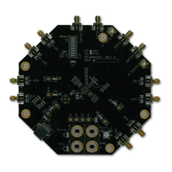
- Page 2 8T49N24x Evaluation Board User Guide Board Overview Use the following diagram to identify and locate: power supply jacks, USB connector, input and output SMA connectors, reset button, EEPROM, etc. Figure 1. Evaluation Board Overview ©2015-2022 Renesas Electronics Corporation April 11, 2022...
- Page 3 8T49N24x- the device to be evaluated OSCI crystal overdrive connector (not installed by default) Crystal connectors (HC49/US through-hole socket and 3.2x2.5 SMD footprint) GPIO test points I2C test points EEPROM socket (AT24C04C) USB connector ©2015-2022 Renesas Electronics Corporation April 11, 2022...
- Page 4 Software GUI Overview The 8T49N24x devices are programmed using Renesas' Timing Commander software, which provides an interactive and intuitive Graphical User Interface to program and adjust the many settings that are available for the devices. Timing Commander is the generic platform upon which many devices' GUIs run on.
- Page 5 8T49N24x Evaluation Board User Guide Schematics The following figures are schematics that are applicable to specific sections of this User Guide. The complete schematics are available in a separate document. Figure 3. Inputs Schematic ©2015-2022 Renesas Electronics Corporation April 11, 2022...
- Page 6 8T49N24x Evaluation Board User Guide Figure 4. Output Termination Schematic ©2015-2022 Renesas Electronics Corporation April 11, 2022...
- Page 7 8T49N24x Evaluation Board User Guide Figure 5. Crystal Interface Schematic ©2015-2022 Renesas Electronics Corporation April 11, 2022...
- Page 8 8T49N24x Evaluation Board User Guide Figure 6. EEPROM/I2C Schematic ©2015-2022 Renesas Electronics Corporation April 11, 2022...
- Page 9 8T49N24x Evaluation Board User Guide Figure 7. DC Control Schematic Figure 8. GPIOs Schematic ©2015-2022 Renesas Electronics Corporation April 11, 2022...
- Page 10 8T49N24x Evaluation Board User Guide Figure 9. VCCO Power Filtering Schematic ©2015-2022 Renesas Electronics Corporation April 11, 2022...
- Page 11 8T49N24x Evaluation Board User Guide Figure 10. VCC Power Filtering Schematic ©2015-2022 Renesas Electronics Corporation April 11, 2022...
- Page 12 8T49N24x Evaluation Board User Guide Figure 11. 8T49N241 and 8T49N242 DUT Schematic ©2015-2022 Renesas Electronics Corporation April 11, 2022...
- Page 13 8T49N24x Evaluation Board User Guide Figure 12. 8T49N240 DUT Schematic ©2015-2022 Renesas Electronics Corporation April 11, 2022...
- Page 14 1. Connect 2.5V to J20 (VCCO_J). 2. Remove R85. This isolates VCCO1 from global VCCO_J. 3. Solder a wire onto test point TP2 and bias with a 1.8V supply. Figure 13. Mixed Output Voltage Operation ©2015-2022 Renesas Electronics Corporation April 11, 2022...
- Page 15 Table 2. Input Termination Schemes Signal AC-coupling capacitors: Frequency CLK0 (C25, C26); CLK1 (C27,C28) Input Signal DC Offset >1MHz Don’t care <1MHz 0 Ω Must meet datasheet Vcmr specs ©2015-2022 Renesas Electronics Corporation April 11, 2022...
- Page 16 Signal Type R35, R36 R40, R41 C21,C22 R37,R38, R42, R43 LVPECL (Default) 0ohm Installed Not Installed LVCMOS 33ohm Not Installed Not Installed LVDS 0ohm Not Installed Not Installed HCSL 33ohm Not Installed Not Installed ©2015-2022 Renesas Electronics Corporation April 11, 2022...
- Page 17 The EEPROM is programmed through Timing Commander. Once connected to the chip using the “Connect to the chip” button in the top-right corner of the window, a button for “Write All” will appear that is used to write all registers to either the 8T49N24x device or the EEPROM. ©2015-2022 Renesas Electronics Corporation April 11, 2022...
- Page 18 “A” for the location of the DIP Switch. The functions for the switches are: ▪ S1: 8T49N24x I2C slave address bit 0 ▪ S2: 8T49N24x I2C slave address bit 1 ▪ S3: 8T49N24x nWP, 0 = Registers write protected, 1 = Normal operation ©2015-2022 Renesas Electronics Corporation April 11, 2022...
- Page 19 Solder a 1uF capacitor onto C18. Note: The input must be AC-coupled. c. R33 may be populated with a 50ohm resistor for input sources requiring such termination. d. Populate R32 with either a 0ohm or 33ohm (LVCMOS) resistor. ©2015-2022 Renesas Electronics Corporation April 11, 2022...
- Page 20 PC ▪ Example settings files and phase noise plots ▪ Tutorial videos for Timing Commander and the 8T49N24x evaluation boards For more questions or support, please submit a technical support request. ©2015-2022 Renesas Electronics Corporation April 11, 2022...
- Page 21 Removed references to 38.88MHz crystal value in the Crystal Interface section. June 6, 2017 ▪ Added support for the 8T49N240i device ▪ Converted the document to the latest template August 6, 2015 Initial release. ©2015-2022 Renesas Electronics Corporation April 11, 2022...
- Page 22 Renesas' products are provided only subject to Renesas' Terms and Conditions of Sale or other applicable terms agreed to in writing. No use of any Renesas resources expands or otherwise alters any applicable warranties or warranty disclaimers for these products.
Need help?
Do you have a question about the 8T49N24 Series and is the answer not in the manual?
Questions and answers