Sign In
Upload
Manuals
Brands
Lattice Semiconductor Manuals
Computer Hardware
CrossLink-NX
Lattice Semiconductor CrossLink-NX Manuals
Manuals and User Guides for Lattice Semiconductor CrossLink-NX. We have
8
Lattice Semiconductor CrossLink-NX manuals available for free PDF download: User Manual, Quick Start Manual, Quick Start
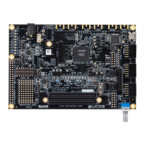
Lattice Semiconductor CrossLink-NX User Manual (54 pages)
PCIe Bridge Board
Brand:
Lattice Semiconductor
| Category:
Network Hardware
| Size: 3 MB
Table of Contents
Table of Contents
3
Acronyms in this Document
6
Introduction
7
Learning Objectives
7
Hardware and Software Requirements
8
Hardware Requirements
8
Software Requirements
8
Setting up the Demo
9
Hardware Setup
9
Jumper Configuration
9
Figure 3.1. Crosslink-NX Pcie Bridge Board Jumper Location
9
Table 3.1. Jumper Configuration
9
Programming the FPGA
10
Figure 3.2. Crosslink-NX Pcie Bridge Board Connection
10
Figure 3.3. Creating a New Project from a Scan
10
Figure 3.4. Radiant Programmer Window
11
Figure 3.5. FPGA Device Settings
11
Figure 3.6. Device Properties Window for SPI Flash Programming
12
Figure 3.7. Programmer Menu Bar
12
Figure 3.8. Programmer Output Window
12
Status LED
13
Figure 3.9. Status LED
13
Table 3.2. Status LED Description
13
Software Setup
14
Software Setup and Installation for Windows
14
Figure 3.10. Running Disable Integrity Checks Command
14
Figure 3.11. Running Test Sign on Command
14
Figure 3.12. Troubleshoot Option
15
Figure 3.13. Advanced Options
15
Figure 3.14. Select Startup Settings
16
Figure 3.15. Restarting Windows
16
Figure 3.16. Welcome Page
17
Figure 3.17. Destination Folder Page
18
Figure 3.18. Summary Page
18
Figure 3.19. Application Installed
19
Figure 3.20. Device Configuration Prompt
19
Figure 3.21. Device Driver Installation Wizard
20
Figure 3.22. Windows Security in Driver Installation
20
Figure 3.23. Device Driver Installation Completed
21
Figure 3.24. Device Manager
21
Figure 3.25. Showing Device Properties
22
Figure 3.26. Hardware Ids of MDIO Device
23
Figure 3.27. Hardware Ids of I C Device
23
Figure 3.28. Hardware Ids of GPIO Device
24
Figure 3.29. Update Driver Menu in Device Manager
25
Figure 3.30. Update Driver Options
25
Figure 3.31. Browse the Driver for Device
26
Figure 3.32. Windows Security in Device Manager
26
Figure 3.33. Driver Installation Status Message
27
Figure 3.34. Multifunction Demo Device Name Displayed in Device Manager
27
Figure 3.35. MDIO, I C, and GPIO Device Drivers in Device Manager
28
Software Setup for Linux
29
Demo Design Overview
32
Theory of Operation
32
Figure 4.1. Relationship of the Hardware and Software Components
32
Design Overview
33
GUI Application
33
Device Drivers
33
Figure 4.2. Pcie Multifunction Demo SW Design
33
Device Hardware (FPGA Design)
34
Figure 4.3. Pcie Multifunction FPGA Design
34
Application Overview
35
Running the PCI Express Demo Application
35
Figure 5.1. Pcie Test Application Device Info Tab
35
Using the PCI Express Demo Application User Interface
36
Functionality Test Tab
36
Gpio
36
Figure 5.2. Functionality Test Tab
36
Figure 5.3. GPIO Input Switch
36
I2C
37
Figure 5.4. GPIO Output Leds
37
Figure 5.5. I2C Bit-Rate Selection
37
Figure 5.6. I2C Address Program
37
Figure 5.7. I2C Master Write
37
Figure 5.8. Single Write to an Arbitrary Address of IMX258-0AQH5 Camera
38
Figure 5.9. Sequential Write Starting from an Arbitrary Address of IMX258-0AQH5 Camera
38
Table 5.1. Master Write Control Description
38
Table 5.2. Registers of MX258-0AQH5 CMOS Camera
38
Figure 5.10. I2C Master Write Procedure
39
Figure 5.11. I2C Master Read
39
Figure 5.12. Single Read from the Held Address of IMX258-0AQH5 Camera
40
Figure 5.13. Sequential Read Starting from the Held Address of IMX258-0AQH5 Camera
40
Figure 5.14. I 2 C Master Write to Write the Register Address
40
Figure 5.15. I C Master Read
41
Figure 5.16. I 2 C Master Register Read
41
Figure 5.17. Single Read from an Arbitrary Address of MX258-0AQH5 Camera
41
Figure 5.18. Sequential Read Starting from an Arbitrary Address of MX258-0AQH5 Camera
41
Table 5.3. Master Register Read Control Description
41
Figure 5.19. I 2 C Master Register Read
42
Figure 5.20. I 2 C Master Register Read
42
Table 5.4. Transaction Log Control Description
42
Figure 5.21. I 2 C Batch Mode Read/Write
43
Table 5.5. Batch Mode Control Description
43
Mdio
44
Figure 5.22. MDIO Phy Addr
44
Figure 5.23. MDIO Configuration Register Read
44
Figure 5.24. MDIO Register Write
44
Figure 5.25. MDIO Configuration through File
45
Figure 5.26. MDIO Configuration File Example
45
Table 5.6. MDIO Batch Mode Control Description
45
Table 5.7. MDIO Batch Mode Table Description
45
Table 5.8. MDIO Input File Description
46
Importing and Building the FPGA Demonstration
47
Hardware Directory Structure
47
Building Lattice Radiant Project
47
Troubleshooting
48
SPI Flash Update
48
Figure 7.1. TCK Frequency Setting
48
Figure 7.2. Port Selection
48
Driver Installation and User Interface Launch for Windows
49
Problem in Driver Installation
49
Problem with Launching User Interface
49
Figure 7.3. User Interface with no Device Driver
49
Driver Installation User Interface Launch for Linux
50
Problem in Driver Loading
50
Figure 7.4. Lspci -Vnm Output Image
50
Problem with User Interface Launching
51
Figure 7.5. Content List of Demonstration/Linux Directory
51
Figure 7.6. Content List of Software/Linux Directory
51
Technical Support Assistance
52
Revision History
53
Advertisement
Lattice Semiconductor CrossLink-NX User Manual (58 pages)
Brand:
Lattice Semiconductor
| Category:
Motherboard
| Size: 3 MB
Table of Contents
Table of Contents
3
Acronyms in this Document
5
1 Introduction
6
Crosslink-NX Evaluation Board
6
Features
6
Figure 1.1. Top View of Crosslink-NX Evaluation Board
7
Figure 1.2. Bottom View of Crosslink-NX Evaluation Board
8
Figure 1.3. Silkscreen of Crosslink-NX Evaluation Board
9
Figure 1.4. Silkscreen of Crosslink-NX Evaluation Board (Bottom)
10
Crosslink-NX Device
11
Applying Power to the Board
11
2 Jumpers and Test Connection
12
Figure 2.1. Top View of Crosslink-NX Evaluation Board - Jumper Locations
12
Table 2.1. Jumper Table
13
3 Power Scheme
14
Figure 3.1. Board Power Scheme
14
Table 3.1. Crosslink-NX VCCIO Supply Options
14
4 Programming and I 2 C
15
JTAG Download Interface
15
Alternate JTAG Download Interface
15
Figure 4.1. Configuration and I
15
Architecture
15
Table 4.1. JTAG Connections
15
Figure 4.2. SPI Flash Operation Dialog
16
JTAG to MSPI Pass-Through Interface
16
SPI Flash Device Selection in Programmer
16
Other JTAG Configuration Pins
17
Table 4.2. Other JTAG Signals
17
5 Crosslink-NX Clock Sources
18
Table 5.1. Clock Sources
18
6 Control Buses - I C, UART, and SPI
19
I 2 C
19
UART Topology
19
Figure 6.1. I 2 C Architecture and UART Options
19
Table 6.1. I 2 C Global Bus Connections
19
SPI Topology
20
SPI Configuration
20
Table 6.2. Crosslink-NX SPI Connections
20
7 Leds and Switches
21
DIP Switch
21
General Purpose Push Buttons
21
Table 7.1. Eight-Position DIP Switch Signals
21
Table 7.2. Push Button Switch Signals
21
General Purpose Leds
22
Indicator Leds
22
Table 7.3. General Purpose LED Signals
22
Table 7.4. Various LED Signals
22
8 Headers/Connectors and LIFCL-40 Device Ball Mapping
23
FMC LPC Connector
23
Table 8.1. FMC LPC Header Pin Connections
23
Parallel FMC Configuration Header
25
Raspberry Pi Board GPIO Header
25
Table 8.2. Parallel FMC Configuration J27 Pin Connections
25
Table 8.3. Raspberry Pi JP8 Header Pin Connections
25
Camera Connector
26
Table 8.4. Camera CN1 Connector Pin Connections
26
D-PHY1 Header
27
Table 8.5. D-PHY1 J6 Header Pin Connections
27
PMOD Header
28
JTAG Header
28
Table 8.6. J17, J18 and J19 Header Pin Connections
28
Table 8.7. J1 Header Pin Connections
28
Parallel Configuration Header
29
ADC Test Header
29
Table 8.8. J27 Header Pin Connections
29
Table 8.9. J26 Header Pin Connections
29
9 Software Requirements
30
10 Storage and Handling
30
11 Ordering Information
30
Table 11.1. Ordering Information
30
Appendix A. Crosslink-NX Evaluation Board Schematics
31
Figure A.1. Title Page
31
Figure A.2. Block Diagram
32
Figure A.3. USB Interface
33
Figure A.4. Camera Interface (Dphys)
34
Figure A.5. Raspberry Pi and User I/O Interface
35
Figure A.6. SERDES Smas/Switches/Fmc Control
36
Figure A.7. I2C Leds and Push Buttons
37
Figure A.8. Pmods
38
Figure A.9. Configuration and ADC
39
Figure A.10. FMC-LPC
40
Figure A.11. Power CSI and Banks
41
Figure A.12. Power Decoupling
42
Figure A.13. Power Regulators
43
Figure A.14. Power Block Diagram
44
Appendix B. Crosslink-NX Evaluation Board Bill of Materials
45
Appendix C. Fast Configuration Issues
53
Appendix D. Schematics Updates for ADC Test
54
References
55
Lattice Semiconductor Documents
55
Technical Support Assistance
56
Revision History
57
Lattice Semiconductor CrossLink-NX User Manual (46 pages)
PCIe Colorbar Demo for Lattice Nexus-based FPGAs
Brand:
Lattice Semiconductor
| Category:
Computer Hardware
| Size: 2 MB
Table of Contents
Table of Contents
3
Acronyms in this Document
6
Introduction
7
Learning Objectives
7
Hardware and Software Requirements
8
Hardware Requirements
8
Software Requirements
8
Setting up the Demo
9
Hardware Setup
9
Figure 3.1. Crosslink-NX Pcie Bridge Board Connection
9
Programming the FPGA
10
Figure 3.2. Certus-NX Pcie Versa Evaluation Board Connection
10
Figure 3.3. Creating a New Project from a Scan
10
Figure 3.4. Lattice Radiant Programmer Window
11
Figure 3.5. Crosslink-NX FPGA Device Settings
11
Figure 3.6. Certus-NX FPGA Device Settings
11
Figure 3.7. Device Properties Window for Crosslink-NX SPI Flash Programming
12
Figure 3.8. Device Properties Window for Certus-NX SPI Flash Programming
13
Figure 3.9. Programmer Menu Bar
13
Figure 3.10. Programmer Output Window
13
Status LED
14
Figure 3.11. Status LED
14
Figure 3.12. Certus-NX Programming Done LED
15
Software Setup
16
Software Setup and Installation for Windows
16
Figure 3.13. Running Disable Integrity Checks Command
16
Figure 3.14. Running Test Sign on Command
16
Figure 3.15. Troubleshoot Option
17
Figure 3.16. Advanced Options
17
Figure 3.17. Select Startup Settings
18
Figure 3.18. Restarting Windows
18
Figure 3.19. Welcome Page
19
Figure 3.20. Destination Folder Page
20
Figure 3.21. Summary Page
20
Figure 3.22. Application Installed
21
Figure 3.23. Device Configuration Prompt
21
Figure 3.24. Device Driver Installation Wizard
22
Figure 3.25. Windows Security in Driver Installation
22
Figure 3.26. Device Driver Installation Completed
23
Figure 3.27. Device Manager
23
Figure 3.28. Showing Device Properties
24
Figure 3.29. Hardware Ids of Crosslink-NX Colorbar Demo Device
24
Figure 3.30. Hardware Ids of Certus-NX Colorbar Demo Device
25
Figure 3.31. Update Driver Menu in Device Manager
26
Figure 3.32. Update Driver Options
26
Figure 3.33. Browse the Driver for Device
27
Figure 3.34. Windows Security in Device Manager
27
Figure 3.35. Crosslink-NX Driver Installation Status Message
28
Figure 3.36. Certus-NX Driver Installation Status Message
28
Figure 3.37. Crosslink-NX Colorbar Demo Device Name Displayed in Device Manager
29
Figure 3.38. Certus-NX Colorbar Demo Device Name Displayed in Device Manager
29
Software Setup for Linux
30
Demo Design Overview
33
Theory of Operation
33
Figure 4.1. Relationship between the Hardware and Software Components
33
Design Overview
34
User Interface Application
34
Driver API
34
Device Drivers
34
Device Hardware (FPGA Design)
34
Figure 4.2. Pcie Colorbar Demo SW Design
34
Figure 4.3. Top Level Architecture of FPGA Design
35
Application Overview
36
Running the Pcie Colorbar Demo Application
36
Figure 5.1. Pcie Colorbar Demo Device Info Tab
36
Pcie Info
37
Figure 5.2. Drop-Down Menu
37
Figure 5.3. Pcie Device Info
37
Play
38
Stop
38
Set Video Param
38
Exit
38
About
38
Figure 5.4. Video Frames
38
Figure 5.5. Set Video Param
38
Importing and Building the FPGA Demonstration
39
Hardware Directory Structure
39
Building Lattice Radiant Project
39
Troubleshooting
40
SPI Flash Update
40
Figure 7.1. TCK Frequency Setting
40
Figure 7.2. Port Selection
40
Driver Installation and User Interface Launch for Windows
41
Problem in Driver Installation
41
Problem with Launching User Interface
41
Figure 7.3. User Interface with no Device Driver
41
Driver Installation User Interface Launch for Linux
42
Problem in Driver Loading
42
Figure 7.4. Error Message
42
Figure 7.5. Lspci -Vnm for Crosslink-NX Output Image
42
Figure 7.6. Lspci -Vnm for Certus-NX Output Image
42
Problem with User Interface Launching
43
Technical Support Assistance
44
Revision History
45
Advertisement
Lattice Semiconductor CrossLink-NX User Manual (22 pages)
ROI User Tracking Using VVML Board Demonstration
Brand:
Lattice Semiconductor
| Category:
Motherboard
| Size: 0 MB
Table of Contents
Table of Contents
3
Acronyms in this Document
5
Introduction
6
Functional Description
6
Figure 2.1. VVML Rev-B Board - Top View
6
Demo Setup
7
Hardware Requirements
7
Software Requirements
7
Programming the Demo
8
Package Folder Structure
8
Load Firmware in FX3 I2C EEPROM
8
Figure 4.1. Demo Package Folder Structure
8
Programming the Crosslink-NX Voice and Vision SPI Flash
9
Erasing the Crosslink-NX Voice and Vision SRAM Prior to Reprogramming
9
Figure 4.2. Selecting FX3 I2C EEPROM in USB Control Centre
9
Figure 4.3. Lattice Radiant Programmer Default Screen
10
Figure 4.4. Lattice Radiant Programmer- Device Selection
10
Figure 4.5. Lattice Radiant Programmer - Device Operation
10
Programming the Crosslink-NX Voice and Vision Board
11
Figure 4.6. Radiant Programmer - Selecting Device Properties Options for Crosslink-NX Flashing
11
Programming Sensai Firmware Binary to the Crosslink-NX Voice and Vision SPI Flash
12
Figure 4.7. Crosslink-NX Voice and Vision Flashing Switch - SW5 Push Button
12
Figure 4.8. Radiant Programmer - Selecting Device Properties Options for Crosslink-NX Flashing
13
Figure 4.9. Radiant Programmer - Output Console
14
Figure 4.10. Radiant Programmer - Selecting Device Properties Options for Crosslink-NX Flashing
15
Figure 4.11. Radiant Programmer - Output Console
16
Running the Demo
17
Figure 5.1. Running the Demo
17
Figure 5.2. Running the Demo
18
Figure 5.3. Running the Demo
18
Ideal Conditions for Testing the Demo
19
Technical Support Assistance
20
Revision History
21
Lattice Semiconductor CrossLink-NX User Manual (18 pages)
QVGA MobileNet Human Counting Using VVML Board
Brand:
Lattice Semiconductor
| Category:
Computer Hardware
| Size: 1 MB
Table of Contents
Table of Contents
3
Acronyms in this Document
4
1 Introduction
5
2 Functional Description
5
Figure 2.1. Top View of Crosslink-NX Voice and Vision Machine Learning Board
5
Figure 2.2. Bottom View of Crosslink-NX Voice and Vision Machine Learning Board
6
3 Demo Setup
7
Hardware Requirements
7
Software Requirements
7
Figure 3.1. Lattice Crosslink-NX Voice and Vision Board
7
4 Programming the Demo
8
Load Firmware in FX3 I C EEPROM
8
Figure 4.1. Selecting FX3 I C EEPROM in USB Control Centre
8
Programming the Crosslink-NX Voice and Vision SPI Flash
9
Erasing the Crosslink-NX Voice and Vision SRAM Prior to Reprogramming
9
Figure 4.2. Radiant Programmer - Default Screen
9
Figure 4.3. Radiant Programmer - Device Selection
9
Programming the Crosslink-NX Voice and Vision Board
10
Figure 4.4. Radiant Programmer - Device Operation
10
Figure 4.5. Radiant Programmer - Selecting Device Properties Options for Crosslink-NX Flashing
11
Figure 4.6. Crosslink-NX Voice and Vision Flashing Switch - SW5 Push Button
12
Figure 4.7. Radiant Programmer - Output Console
12
Programming Sensai Firmware Binary to the Crosslink-NX Voice and Vision SPI Flash
13
Flash Sensai Firmware Hex to Crosslink-NX SPI Flash
13
Figure 4.8. Radiant Programmer - Selecting Device Properties Options for Crosslink-NX Flashing
13
Figure 4.9. Radiant Programmer - Output Console
14
5 Running the Demo
15
Figure 5.1. Running the Demo
15
Technical Support Assistance
16
Revision History
17
Lattice Semiconductor CrossLink-NX User Manual (18 pages)
Brand:
Lattice Semiconductor
| Category:
Motherboard
| Size: 0 MB
Table of Contents
Table of Contents
3
Acronyms in this Document
5
Introduction
6
Functional Description
6
Figure 2.1. VVML Rev-B Board - Top View
6
Demo Setup
7
Hardware Requirements
7
Software Requirements
7
Programming the Demo
8
Package Folder Structure
8
Load Firmware in FX3 I2C EEPROM
8
Figure 4.1. Demo Package Folder Structure
8
Programming the Crosslink-NX Voice and Vision SPI Flash
9
Erasing the Crosslink-NX Voice and Vision SRAM Prior to Reprogramming
9
Figure 4.2. Cypress USB Bootloader - Default Screen
9
Figure 4.3. Radiant Programmer - Default Screen
9
Figure 4.4. Radiant Programmer - Device Selection
9
Programming the Crosslink-NX Voice and Vision Board
10
Figure 4.5. Radiant Programmer - Device Operation
10
Figure 4.6. Radiant Programmer - Selecting Device Properties Options for Crosslink-NX Flashing
11
Figure 4.7. Crosslink-NX Voice and Vision Flashing Switch - SW5 Push Button
12
Figure 4.8. Radiant Programmer - Output Console
12
Programming Sensai Firmware Binary to the Crosslink-NX Voice and Vision SPI Flash
13
Figure 4.9. Radiant Programmer - Selecting Device Properties Options for Crosslink-NX Flashing
13
Figure 4.10. Radiant Programmer - Output Console
14
Running the Demo
15
Run Demo
15
Ideal Conditions for Testing the Demo
15
Figure 5.1. Running the Demo
15
Technical Support Assistance
16
Revision History
17
Lattice Semiconductor CrossLink-NX Quick Start Manual (15 pages)
Object Counting Using VGG
Brand:
Lattice Semiconductor
| Category:
Computer Hardware
| Size: 1 MB
Table of Contents
Table of Contents
3
Acronyms in this Document
4
Introduction
5
Design Process Overview
5
Figure 1.1. Lattice EVDK with Microsd Card Adapter Board
5
Figure 1.2. Lattice Machine Learning Design Flow
6
Machine Training and Creating Frozen File
7
Verifying Tensorflow and Tool Environment
7
Preparing the Dataset
7
Figure 2.1. Tensorflow Installation Check
7
Figure 2.2. Dataset Image Size Check
7
Training the Machine
8
Figure 2.3. Dataset Folder Path Check
8
Figure 2.4. Dataset List, Image, and Label Data Path
8
Figure 2.5. Create a Label File
8
Figure 2.6. Execute the Script
9
Figure 2.7. Tensorboard - Generated Link
9
Figure 2.8. Training Status
9
Figure 2.9. Image Menu
10
Figure 2.10. Checkpoint Data Files at Log Folder
10
Generating Frozen (*.Pb) File
11
Figure 2.11. Create *.Pbtxt File
11
Figure 2.12. Check Frozen File
11
Generating the Binary File
12
Programming the Bitstream and Binary Files to VIP Board and SD Card
12
Technical Support Assistance
13
Revision History
14
Lattice Semiconductor CrossLink-NX Quick Start (2 pages)
Voice and Vision Machine Learning Board
Brand:
Lattice Semiconductor
| Category:
Control Unit
| Size: 0 MB
Table of Contents
Check Kit Contents
1
Preparing the Hardware and Running the Demonstration
1
Set SW1 Inputs to the 1000 Setting (on Side=0)
2
Technical Support
2
Advertisement
Related Products
Lattice Semiconductor CrossLink-NX ISP Demo
Lattice Semiconductor CertusPro-NX
Lattice Semiconductor CertusPro-NX Versa Board
Lattice Semiconductor CrossLink
Lattice Semiconductor iCE40 SPRAM Series
Lattice Semiconductor iCE40 Ultra
Lattice Semiconductor LatticeMico GPIO
Lattice Semiconductor LatticeMico32
Lattice Semiconductor LatticeMico8
Lattice Semiconductor sysCLOCK ECP5
Lattice Semiconductor Categories
Motherboard
Computer Hardware
Microcontrollers
Controller
Recording Equipment
More Lattice Semiconductor Manuals
Login
Sign In
OR
Sign in with Facebook
Sign in with Google
Upload manual
Upload from disk
Upload from URL