Lattice Semiconductor CrossLink-NX User Manual
Pcie bridge board
Hide thumbs
Also See for CrossLink-NX:
- User manual (58 pages) ,
- Quick start manual (15 pages) ,
- Quick start (2 pages)

Related Manuals for Lattice Semiconductor CrossLink-NX


Summary of Contents for Lattice Semiconductor CrossLink-NX
- Page 1 CrossLink-NX PCIe Bridge Board Multifunction Demo User Guide FPGA-UG-02150-1.0 February 2022...
- Page 2 The information provided in this document is proprietary to Lattice Semiconductor, and Lattice reserves the right to make any changes to the information in this document or to any products at any time without notice.
-
Page 3: Table Of Contents
Revision History .................................. 53 © 2022 Lattice Semiconductor Corp. All Lattice trademarks, registered trademarks, patents, and disclaimers are as listed at www.latticesemi.com/legal. All other brand or product names are trademarks or registered trademarks of their respective holders. The specifications and information herein are subject to change without notice. - Page 4 C Master Write to Write the Register Address ..................... 40 © 2022 Lattice Semiconductor Corp. All Lattice trademarks, registered trademarks, patents, and disclaimers are as listed at www.latticesemi.com/legal. All other brand or product names are trademarks or registered trademarks of their respective holders. The specifications and information herein are subject to change without notice.
- Page 5 Table 5.8. MDIO Input File Description ..........................46 © 2022 Lattice Semiconductor Corp. All Lattice trademarks, registered trademarks, patents, and disclaimers are as listed at www.latticesemi.com/legal. All other brand or product names are trademarks or registered trademarks of their respective holders. The specifications and information herein are subject to change without notice.
-
Page 6: Acronyms In This Document
General Purpose Input Output © 2022 Lattice Semiconductor Corp. All Lattice trademarks, registered trademarks, patents, and disclaimers are as listed at www.latticesemi.com/legal. All other brand or product names are trademarks or registered trademarks of their respective holders. The specifications and information herein are subject to change without notice. -
Page 7: Introduction
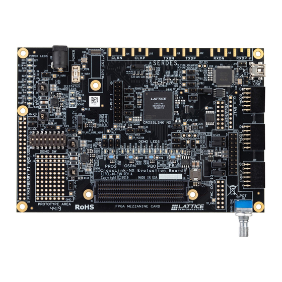
Lattice Nexus FPGA platform using low power 28 nm FDSOI technology. The board can expand the usability of the CrossLink-NX FPGA with 2.5 Gbps Hardened MIPI D-PHY, 5 Gbps PCIe, 1.5 Gbps programmable I/O, DDR3, USB 3.0, Ethernet, and SGMII. Board resources such as jumpers, LED indicators, push buttons, and switches are available for user-defined applications. -
Page 8: Hardware And Software Requirements
Bit file for the CrossLink-NX board SPI Flash (LIFCL40_PCIe_MultiFunction.bit) © 2022 Lattice Semiconductor Corp. All Lattice trademarks, registered trademarks, patents, and disclaimers are as listed at www.latticesemi.com/legal. All other brand or product names are trademarks or registered trademarks of their respective holders. The specifications and information herein are subject to change without notice. -
Page 9: Setting Up The Demo
CrossLink-NX PCIe Bridge Board Multifunction Demo User Guide 3. Setting Up the Demo 3.1. Hardware Setup This section covers the steps in programming the demo to the SPI memory of the CrossLink-NX PCIe Bridge Board. 3.1.1. Jumper Configuration Install the jumpers listed in Table 3.1. -
Page 10: Programming The Fpga
Figure 3.3. Creating a New Project from a Scan © 2022 Lattice Semiconductor Corp. All Lattice trademarks, registered trademarks, patents, and disclaimers are as listed at www.latticesemi.com/legal. All other brand or product names are trademarks or registered trademarks of their respective holders. The specifications and information herein are subject to change without notice. -
Page 11: Figure 3.4. Radiant Programmer Window
3. Double-click under Operation to open the Device Properties dialog box. © 2022 Lattice Semiconductor Corp. All Lattice trademarks, registered trademarks, patents, and disclaimers are as listed at www.latticesemi.com/legal. All other brand or product names are trademarks or registered trademarks of their respective holders. The specifications and information herein are subject to change without notice. -
Page 12: Figure 3.6. Device Properties Window For Spi Flash Programming
If the programming operation was not successful, please refer to the troubleshooting section of this document. © 2022 Lattice Semiconductor Corp. All Lattice trademarks, registered trademarks, patents, and disclaimers are as listed at www.latticesemi.com/legal. All other brand or product names are trademarks or registered trademarks of their respective holders. The specifications and information herein are subject to change without notice. -
Page 13: Status Led
Green: Lights if configuration is successful © 2022 Lattice Semiconductor Corp. All Lattice trademarks, registered trademarks, patents, and disclaimers are as listed at www.latticesemi.com/legal. All other brand or product names are trademarks or registered trademarks of their respective holders. The specifications and information herein are subject to change without notice. -
Page 14: Software Setup
3. Close the Command Prompt and restart your PC. © 2022 Lattice Semiconductor Corp. All Lattice trademarks, registered trademarks, patents, and disclaimers are as listed at www.latticesemi.com/legal. All other brand or product names are trademarks or registered trademarks of their respective holders. The specifications and information herein are subject to change without notice. -
Page 15: Figure 3.12. Troubleshoot Option
Figure 3.13. Advanced Options © 2022 Lattice Semiconductor Corp. All Lattice trademarks, registered trademarks, patents, and disclaimers are as listed at www.latticesemi.com/legal. All other brand or product names are trademarks or registered trademarks of their respective holders. The specifications and information herein are subject to change without notice. -
Page 16: Figure 3.14. Select Startup Settings
Install manually © 2022 Lattice Semiconductor Corp. All Lattice trademarks, registered trademarks, patents, and disclaimers are as listed at www.latticesemi.com/legal. All other brand or product names are trademarks or registered trademarks of their respective holders. The specifications and information herein are subject to change without notice. -
Page 17: Figure 3.16. Welcome Page
3. Provide the location where you want to install the application. Click Next. © 2022 Lattice Semiconductor Corp. All Lattice trademarks, registered trademarks, patents, and disclaimers are as listed at www.latticesemi.com/legal. All other brand or product names are trademarks or registered trademarks of their respective holders. The specifications and information herein are subject to change without notice. -
Page 18: Figure 3.17. Destination Folder Page
Figure 3.18. Summary Page © 2022 Lattice Semiconductor Corp. All Lattice trademarks, registered trademarks, patents, and disclaimers are as listed at www.latticesemi.com/legal. All other brand or product names are trademarks or registered trademarks of their respective holders. The specifications and information herein are subject to change without notice. -
Page 19: Figure 3.19. Application Installed
Figure 3.20. Device Configuration Prompt © 2022 Lattice Semiconductor Corp. All Lattice trademarks, registered trademarks, patents, and disclaimers are as listed at www.latticesemi.com/legal. All other brand or product names are trademarks or registered trademarks of their respective holders. The specifications and information herein are subject to change without notice. -
Page 20: Figure 3.21. Device Driver Installation Wizard
3.23. © 2022 Lattice Semiconductor Corp. All Lattice trademarks, registered trademarks, patents, and disclaimers are as listed at www.latticesemi.com/legal. All other brand or product names are trademarks or registered trademarks of their respective holders. The specifications and information herein are subject to change without notice. -
Page 21: Figure 3.23. Device Driver Installation Completed
Figure 3.24. Device Manager © 2022 Lattice Semiconductor Corp. All Lattice trademarks, registered trademarks, patents, and disclaimers are as listed at www.latticesemi.com/legal. All other brand or product names are trademarks or registered trademarks of their respective holders. The specifications and information herein are subject to change without notice. -
Page 22: Figure 3.25. Showing Device Properties
GPIO: PCI\VEN_1204&DEV_9C20&SUBSYS_E00419AA © 2022 Lattice Semiconductor Corp. All Lattice trademarks, registered trademarks, patents, and disclaimers are as listed at www.latticesemi.com/legal. All other brand or product names are trademarks or registered trademarks of their respective holders. The specifications and information herein are subject to change without notice. -
Page 23: Figure 3.26. Hardware Ids Of Mdio Device
C Device © 2022 Lattice Semiconductor Corp. All Lattice trademarks, registered trademarks, patents, and disclaimers are as listed at www.latticesemi.com/legal. All other brand or product names are trademarks or registered trademarks of their respective holders. The specifications and information herein are subject to change without notice. -
Page 24: Figure 3.28. Hardware Ids Of Gpio Device
Figure 3.28. Hardware IDs of GPIO Device © 2022 Lattice Semiconductor Corp. All Lattice trademarks, registered trademarks, patents, and disclaimers are as listed at www.latticesemi.com/legal. All other brand or product names are trademarks or registered trademarks of their respective holders. The specifications and information herein are subject to change without notice. -
Page 25: Figure 3.29. Update Driver Menu In Device Manager
Figure 3.30. Update Driver Options © 2022 Lattice Semiconductor Corp. All Lattice trademarks, registered trademarks, patents, and disclaimers are as listed at www.latticesemi.com/legal. All other brand or product names are trademarks or registered trademarks of their respective holders. The specifications and information herein are subject to change without notice. -
Page 26: Figure 3.31. Browse The Driver For Device
Figure 3.32. Windows Security in Device Manager © 2022 Lattice Semiconductor Corp. All Lattice trademarks, registered trademarks, patents, and disclaimers are as listed at www.latticesemi.com/legal. All other brand or product names are trademarks or registered trademarks of their respective holders. The specifications and information herein are subject to change without notice. -
Page 27: Figure 3.33. Driver Installation Status Message
Device Manager as shown in Figure 7.28 © 2022 Lattice Semiconductor Corp. All Lattice trademarks, registered trademarks, patents, and disclaimers are as listed at www.latticesemi.com/legal. All other brand or product names are trademarks or registered trademarks of their respective holders. The specifications and information herein are subject to change without notice. -
Page 28: Figure 3.35. Mdio, I C, And Gpio Device Drivers In Device Manager
C, and GPIO Device Drivers in Device Manager © 2022 Lattice Semiconductor Corp. All Lattice trademarks, registered trademarks, patents, and disclaimers are as listed at www.latticesemi.com/legal. All other brand or product names are trademarks or registered trademarks of their respective holders. The specifications and information herein are subject to change without notice. -
Page 29: Software Setup For Linux
© 2022 Lattice Semiconductor Corp. All Lattice trademarks, registered trademarks, patents, and disclaimers are as listed at www.latticesemi.com/legal. All other brand or product names are trademarks or registered trademarks of their respective holders. The specifications and information herein are subject to change without notice. - Page 30 This builds the driver and API library. © 2022 Lattice Semiconductor Corp. All Lattice trademarks, registered trademarks, patents, and disclaimers are as listed at www.latticesemi.com/legal. All other brand or product names are trademarks or registered trademarks of their respective holders. The specifications and information herein are subject to change without notice.
- Page 31 ./MFDemo.sh © 2022 Lattice Semiconductor Corp. All Lattice trademarks, registered trademarks, patents, and disclaimers are as listed at www.latticesemi.com/legal. All other brand or product names are trademarks or registered trademarks of their respective holders. The specifications and information herein are subject to change without notice.
-
Page 32: Demo Design Overview
Figure 4.1. Relationship of the Hardware and Software Components © 2022 Lattice Semiconductor Corp. All Lattice trademarks, registered trademarks, patents, and disclaimers are as listed at www.latticesemi.com/legal. All other brand or product names are trademarks or registered trademarks of their respective holders. The specifications and information herein are subject to change without notice. -
Page 33: Design Overview
© 2022 Lattice Semiconductor Corp. All Lattice trademarks, registered trademarks, patents, and disclaimers are as listed at www.latticesemi.com/legal. All other brand or product names are trademarks or registered trademarks of their respective holders. The specifications and information herein are subject to change without notice. -
Page 34: Device Hardware (Fpga Design)
Figure 4.3. PCIe Multifunction FPGA Design © 2022 Lattice Semiconductor Corp. All Lattice trademarks, registered trademarks, patents, and disclaimers are as listed at www.latticesemi.com/legal. All other brand or product names are trademarks or registered trademarks of their respective holders. The specifications and information herein are subject to change without notice. -
Page 35: Application Overview
Figure 5.1. PCIe Test Application Device Info Tab © 2022 Lattice Semiconductor Corp. All Lattice trademarks, registered trademarks, patents, and disclaimers are as listed at www.latticesemi.com/legal. All other brand or product names are trademarks or registered trademarks of their respective holders. The specifications and information herein are subject to change without notice. -
Page 36: Using The Pci Express Demo Application User Interface
5.4. © 2022 Lattice Semiconductor Corp. All Lattice trademarks, registered trademarks, patents, and disclaimers are as listed at www.latticesemi.com/legal. All other brand or product names are trademarks or registered trademarks of their respective holders. The specifications and information herein are subject to change without notice. -
Page 37: I2C
C Master Write © 2022 Lattice Semiconductor Corp. All Lattice trademarks, registered trademarks, patents, and disclaimers are as listed at www.latticesemi.com/legal. All other brand or product names are trademarks or registered trademarks of their respective holders. The specifications and information herein are subject to change without notice. -
Page 38: Figure 5.8. Single Write To An Arbitrary Address Of Imx258-0Aqh5 Camera
LINE_LENGTH_PCK [15:8] © 2022 Lattice Semiconductor Corp. All Lattice trademarks, registered trademarks, patents, and disclaimers are as listed at www.latticesemi.com/legal. All other brand or product names are trademarks or registered trademarks of their respective holders. The specifications and information herein are subject to change without notice. -
Page 39: Figure 5.10. I2C Master Write Procedure
Figure 5.13 shows the format for a sequential read starting from the held address. © 2022 Lattice Semiconductor Corp. All Lattice trademarks, registered trademarks, patents, and disclaimers are as listed at www.latticesemi.com/legal. All other brand or product names are trademarks or registered trademarks of their respective holders. The specifications and information herein are subject to change without notice. -
Page 40: Figure 5.12. Single Read From The Held Address Of Imx258-0Aqh5 Camera
C Master Write to Write the Register Address © 2022 Lattice Semiconductor Corp. All Lattice trademarks, registered trademarks, patents, and disclaimers are as listed at www.latticesemi.com/legal. All other brand or product names are trademarks or registered trademarks of their respective holders. The specifications and information herein are subject to change without notice. -
Page 41: Figure 5.15. I C Master Read
4. Select the 7-bit mode radio button. © 2022 Lattice Semiconductor Corp. All Lattice trademarks, registered trademarks, patents, and disclaimers are as listed at www.latticesemi.com/legal. All other brand or product names are trademarks or registered trademarks of their respective holders. The specifications and information herein are subject to change without notice. -
Page 42: Figure 5.19. I 2 C Master Register Read
Specifies the transferred data during the transaction. © 2022 Lattice Semiconductor Corp. All Lattice trademarks, registered trademarks, patents, and disclaimers are as listed at www.latticesemi.com/legal. All other brand or product names are trademarks or registered trademarks of their respective holders. The specifications and information herein are subject to change without notice. -
Page 43: Figure 5.21. I 2 C Batch Mode Read/Write
Used to stop the execution of the batch file. © 2022 Lattice Semiconductor Corp. All Lattice trademarks, registered trademarks, patents, and disclaimers are as listed at www.latticesemi.com/legal. All other brand or product names are trademarks or registered trademarks of their respective holders. The specifications and information herein are subject to change without notice. -
Page 44: Mdio
‘Addr’ and press the ‘Read’ button. The ‘Value’ text box will be updated to show the data read from the specified address. For the Crosslink-NX PCIe Bridge Board, the PHY is the DP83867 Ethernet Phy, and address 0x0 contains the default value of 0x1140 which should appear after clicking ‘Read’. -
Page 45: Figure 5.25. Mdio Configuration Through File
Figure 5.26. MDIO Configuration File Example © 2022 Lattice Semiconductor Corp. All Lattice trademarks, registered trademarks, patents, and disclaimers are as listed at www.latticesemi.com/legal. All other brand or product names are trademarks or registered trademarks of their respective holders. The specifications and information herein are subject to change without notice. -
Page 46: Table 5.8. Mdio Input File Description
© 2022 Lattice Semiconductor Corp. All Lattice trademarks, registered trademarks, patents, and disclaimers are as listed at www.latticesemi.com/legal. All other brand or product names are trademarks or registered trademarks of their respective holders. The specifications and information herein are subject to change without notice. -
Page 47: Importing And Building The Fpga Demonstration
CrossLink-NX PCIe Bridge Board Multifunction Demo User Guide 6. Importing and Building the FPGA Demonstration The package includes the PCIe IP, .bit file, and synthesis projects using Lattice Radiant Software for the CrossLink-NX PCIe Bridge board. 6.1. Hardware Directory Structure The Hardware folder inside the package contains the following subfolders. -
Page 48: Troubleshooting
Figure 7.2. Port Selection © 2022 Lattice Semiconductor Corp. All Lattice trademarks, registered trademarks, patents, and disclaimers are as listed at www.latticesemi.com/legal. All other brand or product names are trademarks or registered trademarks of their respective holders. The specifications and information herein are subject to change without notice. -
Page 49: Driver Installation And User Interface Launch For Windows
Demo/bin folder. © 2022 Lattice Semiconductor Corp. All Lattice trademarks, registered trademarks, patents, and disclaimers are as listed at www.latticesemi.com/legal. All other brand or product names are trademarks or registered trademarks of their respective holders. The specifications and information herein are subject to change without notice. -
Page 50: Driver Installation User Interface Launch For Linux
If the driver does not build properly, check for any software or kernel dependencies. © 2022 Lattice Semiconductor Corp. All Lattice trademarks, registered trademarks, patents, and disclaimers are as listed at www.latticesemi.com/legal. All other brand or product names are trademarks or registered trademarks of their respective holders. The specifications and information herein are subject to change without notice. -
Page 51: Problem With User Interface Launching
./MFDemo.sh © 2022 Lattice Semiconductor Corp. All Lattice trademarks, registered trademarks, patents, and disclaimers are as listed at www.latticesemi.com/legal. All other brand or product names are trademarks or registered trademarks of their respective holders. The specifications and information herein are subject to change without notice. -
Page 52: Technical Support Assistance
Submit a technical support case through www.latticesemi.com/techsupport. © 2022 Lattice Semiconductor Corp. All Lattice trademarks, registered trademarks, patents, and disclaimers are as listed at www.latticesemi.com/legal. All other brand or product names are trademarks or registered trademarks of their respective holders. The specifications and information herein are subject to change without notice. -
Page 53: Revision History
Initial release. © 2022 Lattice Semiconductor Corp. All Lattice trademarks, registered trademarks, patents, and disclaimers are as listed at www.latticesemi.com/legal. All other brand or product names are trademarks or registered trademarks of their respective holders. The specifications and information herein are subject to change without notice. - Page 54 www.latticesemi.com...
Need help?
Do you have a question about the CrossLink-NX and is the answer not in the manual?
Questions and answers