Advertisement
Quick Links
NCP45492IMNGEVB
NCP45492 Evaluation Board
User's Manual
Introduction
This user's manual provides detailed information
regarding
the
configuration
NCP45492IMNGEVB Evaluation board. The evaluation
board serves as a demonstration of NCP45492 general
functionality for single chip mode featuring power
monitoring of 4 channels. The evaluation board also
provides a means of quick prototyping for specific
applications.
Features
•
NCP45492
•
Connectors for 4 High Current Supplies and Loads
•
Configuration Options for Shunt Current and Gain
Settings
•
Appropriate Test Loops for Easy Evaluations
QUICK START
Recommended Equipment
Before beginning, the following equipment is needed:
•
4 DC Power Supplies (2 capable of at least 7 V, 2 capable
of at least 13 V to support current evaluation board setup)
•
4 DC Loads (up to at least 2 A)
•
Function Generator
•
Oscilloscope
•
Digital Multi−meter
•
SMA to BNC Cables Recommended for Connection to
DIFF_OUTN, DIFF_OUTP, and MUX_SEL
Board Setup
The assembled evaluation board targets Bus Voltages and
Shunt Currents shown in Tables 1 and 2. VBUS1 ties to both
channel 1 and channel 3 bus voltage inputs. VBUS2 ties to
both channel 2 and channel 4 bus voltage inputs. Refer to the
schematic and layout diagrams found in
Appendix B
respectively as needed.
Table 1. BUS VOLTAGE SETUP
Channel
Target Bus Voltage
1 (VBUS1)
2 (VBUS2)
3 (VBUS1)
4 (VBUS2)
© Semiconductor Components Industries, LLC, 2019
January, 2019 − Rev. 0
and
use
of
Appendix A
Bus Divider
12 V
1/60 V/V
6 V
1/30 V/V
12 V
1/60 V/V
6 V
1/30 V/V
the
EVAL BOARD USER'S MANUAL
Table 2. SHUNT CURRENT SETUP
Channel
Load 1
Load 2
Load 3
Load 4
The specific resistor configuration populated on the board
facilitate these gain settings. The nominal differential
amplifier gain is 2 V/V. Therefore, the expected differential
output for any channels voltage or current can be calculated
as follows:
•
For Bus Voltage:
Diff Output + Bus Voltage @
•
For Load Current:
Diff Output = Load Current * Channel Shunt Gain * 2
Diff Output + I
and
These gain settings can be adjusted by changing the bus
divider resistors, and the shunt current network resistors as
desired.
Board Connections & Jumper Settings
The following board to bench equipment connections are
required for demonstration of 4 channel power monitoring.
Make all board connections with supplies and loads
disabled. Take adequate precautions when working with
high current and high voltage applications. Table 3 below
defines all default board connections and their purpose.
1
www.onsemi.com
Shunt Current
Shunt Gain
0.5 A
400 mV/A
5 A
40 mV/A
0.5 A
400 mV/A
5 A
40 mV/A
R4
@ 2
R4 ) R3
R2 ) R
sense
@
@ 2
Load
R1
Publication Order Number:
EVBUM2605/D
(eq. 1)
(eq. 2)
Advertisement

Related Manuals for ON Semiconductor NCP45492IMNGEVB


Summary of Contents for ON Semiconductor NCP45492IMNGEVB
- Page 1 User's Manual Introduction This user’s manual provides detailed information regarding configuration NCP45492IMNGEVB Evaluation board. The evaluation www.onsemi.com board serves as a demonstration of NCP45492 general EVAL BOARD USER’S MANUAL functionality for single chip mode featuring power monitoring of 4 channels. The evaluation board also provides a means of quick prototyping for specific applications.
- Page 2 NCP45492IMNGEVB Table 3. EVALUATION BOARD DEFAULT CONNECTIONS Connection Connect To0 Purpose VBUS1 (banana) 12 V supply Provides channel 1 and channel 3 bus voltages VBUS2 (banana) 6 V supply Provides channel 2 and channel 4 bus voltages LOAD1 & GND (banana) 0.5 A load current (24 W 1W resistor)
-
Page 3: Appendix A − Evaluation Board Schematic
NCP45492IMNGEVB Testing Procedure 5. Observe the following: The NCP45492IMNGEVB comes fully assembled and a. 1.3 V on BG_REF_OUT tested. Follow the steps below to verify board operation. b. 650 mV on CM_REF_IN Refer to the schematic and layout diagrams found in c. -
Page 4: Appendix B − Bill Of Materials
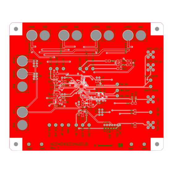
NCP45492IMNGEVB APPENDIX B − BILL OF MATERIALS Table 5. BILL OF MATERIALS Footprint Value Quantity Digikey P/N Designator BG_REF_OUT, BS_IN1, BS_IN2, BS_IN3, Test_Point Test loop 36−5009−ND BS_IN4, BS_OK, BS_REF, CM_REF_IN, DIFF_OUTN, DIFF_OUTP, GND2, GND3, GND4, GND5, GND6, SH_IN1, SH_IN2, SH_IN3, SH_IN4, SH_O1, SH_O2, SH_O3,... - Page 5 NCP45492IMNGEVB APPENDIX C − NCP45492 EVALUATION BOARD LAYOUT Figure 2. PCB Front (Top Metallization) www.onsemi.com...
-
Page 6: Technical Support
onsemi, , and other names, marks, and brands are registered and/or common law trademarks of Semiconductor Components Industries, LLC dba “onsemi” or its affiliates and/or subsidiaries in the United States and/or other countries. onsemi owns the rights to a number of patents, trademarks, copyrights, trade secrets, and other intellectual property. A listing of onsemi’s product/patent coverage may be accessed at www.onsemi.com/site/pdf/Patent−Marking.pdf.
Need help?
Do you have a question about the NCP45492IMNGEVB and is the answer not in the manual?
Questions and answers