Advertisement
NCP2824FCT2GEVB
NCP2824FCT2 Evaluation
Board User's Manual
Overview
The NCP2824 is a Filterless Class D amplifier capable of
delivering up to 2.4 W to a 4 W load with a 5 V supply
voltage. With the same battery voltage, it can deliver 1.2 W
to an 8 W load with less than 1% THD+N. The Non-clipping
function adjusts automatically the output voltage in order to
control the distortion when an excessive input is applied to
the amplifier. This adjustment is done thanks to an
Automatic Gain Control circuitry (AGC) built-in the chip.
A simple Single wire interface allows to enable/disable the
© Semiconductor Components Industries, LLC, 2012
May, 2012 − Rev. 2
non Clipping function and also to configure the maximum
distortion level in the output. A programmable power limit
function is also embedded in order to protect speakers from
damage caused by an excessive sound level.
operation of the NCP2824 device for laboratory
characterization. The NCP2824FCT2GEVB schematic is
depicted in Figure 2.
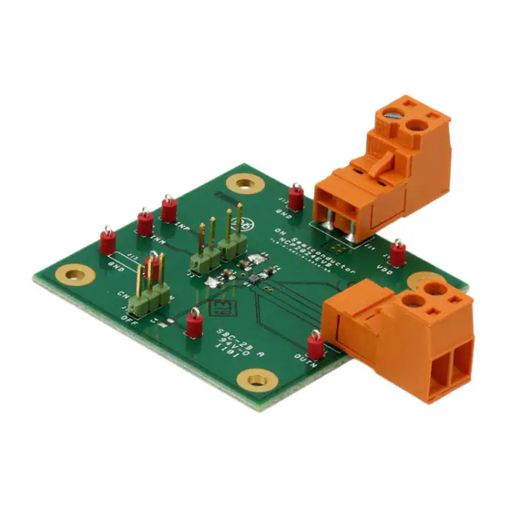
Figure 1. NCP2824FCT2GEVB Board Picture
1
http://onsemi.com
EVAL BOARD USER'S MANUAL
The intent of the evaluation boards is to illustrate typical
Publication Order Number:
EVBUM2110/D
Advertisement
Table of Contents

Subscribe to Our Youtube Channel
Related Manuals for ON Semiconductor NCP2824FCT2GEVB


Summary of Contents for ON Semiconductor NCP2824FCT2GEVB
- Page 1 NCP2824 device for laboratory control the distortion when an excessive input is applied to the amplifier. This adjustment is done thanks to an characterization. The NCP2824FCT2GEVB schematic is Automatic Gain Control circuitry (AGC) built-in the chip. depicted in Figure 2.
-
Page 2: Board - Schematic
Î Î CNTL Jumper3 Î Î Î Î Î Î Î Î Î Î Î Î TP 1.0D ENABLE− SINGLE WIRE Title NCP2824 EVB Size Document Number Custom NCP2824 EVB TLS−P−001−A−0310−DR Date: Sheet Figure 2. NCP2824FCT2GEVB Evaluation Board Schematic http://onsemi.com... -
Page 3: Operation
NCP2824FCT2GEVB OPERATION The operating power supply of the NCP2824 is from 2.5 Table 1. NCP2824 CONFIGURATION to 5.5 V. The absolute maximum input voltage is 7.0 V. A Pulse power supply set to 3.6 V and current limit set to at least... - Page 4 NCP2824FCT2GEVB Table 2. BOARD CONNECTIONS INPUT POWER Symbol Descriptions J14−1 This is the positive connection for power supply. The leads (positive + ground) to the input supply should be twisted and kept as short as possible. J14−2 This is the return connection for the power supply (Ground signal)
-
Page 5: Typical Operating Characteristics
NCP2824FCT2GEVB TYPICAL OPERATING CHARACTERISTICS THD+N vs Pout @ 255C THD+N vs Pout @ 25°C Vdd=2.5V Vdd=2.7V Vdd=3V Vdd=3.6V Vdd=4.2V Vdd=5V Vdd=5.5V Vdd=2.5V Vdd=2.7V Vdd=3V Vdd=3.6V Vdd=4.2V Vdd=5V Vdd=5.5V 0.01 0.01 1000 10000 1000 10000 Pout (mW) Pout (mW) Figure 3. THD vs. P , RI = 8 W, f = 1 kHz Figure 4. -
Page 6: Pcb Layout
NCP2824FCT2GEVB PCB LAYOUT As with all Class D amplifiers, care must be observed to Figure 11 show the layout of the NCP2824FCT2GEVB place the components on the PCB and layout the critical board. nodes. The evaluation board is made of 4 PCB layers where For more specific layout guidelines please refer to the first internal layer is a GND. - Page 7 PUBLICATION ORDERING INFORMATION LITERATURE FULFILLMENT: N. American Technical Support: 800−282−9855 Toll Free ON Semiconductor Website: www.onsemi.com Literature Distribution Center for ON Semiconductor USA/Canada Order Literature: http://www.onsemi.com/orderlit P.O. Box 5163, Denver, Colorado 80217 USA Europe, Middle East and Africa Technical Support: Phone: 303−675−2175 or 800−344−3860 Toll Free USA/Canada...
Need help?
Do you have a question about the NCP2824FCT2GEVB and is the answer not in the manual?
Questions and answers