
Subscribe to Our Youtube Channel
Related Manuals for DTK PAM-0052V


Summary of Contents for DTK PAM-0052V
- Page 1 PAM-0052V High Performance Pentium PCI Mainboard Edition 1.30 1999 DTK Computer, Inc. P/N: 155100-8755...
- Page 2 WARNING For the system to operate normally, please make sure JP6 of the mainboard is set as below. Refer to Fig. 3 in this manual for the location JP6. If JP6 is shorted to 2-3, no CMOS data can be retained. CAUTION The motherboard is an electrostatic sensitive device.
-
Page 3: Table Of Contents
CONTENTS CHAPTER 1 INTRODUCTION CHAPTER 2 JUMPER SETTINGS JUMPERS PRESENTATION CPU TYPE 2.2.1 INTEL PENTIUM w/ MMX™ TECH (P55C) CPU 2.2.2 AMD-K6 CPU 2.2.3 CYRIX 6x86L CPU 2.2.4 CYRIX 6x86MX CPU GRAPHICAL DESCRIPTION OF JUMPER SETTINGS CPU VOLTAGE CPU TO BUS FREQUENCY RATIO (SW1-4,5,6) CPU EXTERNAL (BUS) FREQUENCY SELECTION (SW1-7,8,9,10) SDRAM FREQUENCY SELECTION (SW-10) CPU SPEED... - Page 4 4.10 USER PASSWORD 4.11 IDE HDD AUTO DETECTION 4.12 SAVE & EXIT SETUP MENU 4.13 EXIT WITHOUT SAVING MENU CHAPTER 5 FLASH AND DMI UTILITY AWARD FLASH UTILITY DESKTOP MANAGEMENT INTERFACE (DMI) OVERVIEW APPENDIX A QUICK GUIDE...
-
Page 5: Introduction
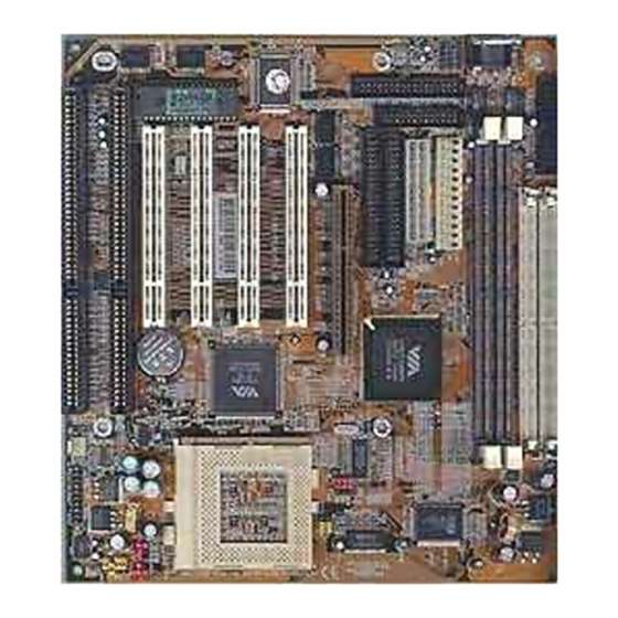
CHAPTER 1 INTRODUCTION Preface The motherboard is a 4-layer, 2/3 baby AT size high performance mainboard. It includes VIA VT82C598MVP (MVP3) system chipset, Winbond W83877F super I/O chip. Features Processor • Intel Pentium/MMX, Cyrix 6x86L/6x86MX/M II and AMD K6/K6-2 CPU. •... - Page 6 Chapter 1 Fig. 1 Key Components of the Mainboard System BIOS • Award BIOS (128KB Flash EPROM). Slots • Four PCI slots • Two ISA slots Form Factor • 2/3 Baby AT size (220mm x 230mm)
- Page 7 Introduction Environment Working Specifications Actual Field MTBF (hours) 104,515 hours Preventive Maintenance Not Required Environmental Limits Operating Non-operating Temperature 0 to 50 degree Celsius -10 to 65 Degree Celsius Relative Humidity (without condensation) 8 to 85% 5 to 95% Altitude 10,000ft 40,000ft Vibration...
- Page 8 Chapter 1...
-
Page 9: Jumper Settings
CHAPTER 2 JUMPER SETTINGS JUMPERS PRESENTATION Pins 1 and 2 are shorted with a jumper cap. Pins 2 and 3 are shorted with a jumper cap. The jumper is shorted when the jumper cap is placed over the two pins of the jumper. The jumper is open when the jumper cap is removed from jumper. -
Page 10: Amd-K6 Cpu
Chapter 2 2.2.2 AMD-K6 CPU The AMD-K6 CPU family require dual voltage power for operation. The AMD- K6/166, 200 require a voltage of 2.9V core and 3.3V I/O. The AMD-K6/233 require a voltage of 3.2V core and 3.3V I/O. (The following diagram is provided as an example only. -
Page 11: Cyrix 6X86Mx Cpu
Jumper Settings 2.2.4 CYRIX 6x86MX CPU The Cyrix 6x86MX has different I/O and Core Voltage. Please refer to the CPU marking. Fig. 2d CPU Description (Top Side) I/O Voltage Core Voltage Cyrix 6x86MX 3.3V 2.9V Cyrix 6x86L 3.3V 2.8V... -
Page 12: Graphical Description Of Jumper Settings
Chapter 2 GRAPHICAL DESCRIPTION OF JUMPER SETTINGS Fig. 3 Jumper Location of the mainboard... -
Page 13: Cpu Voltage
Jumper Settings CPU VOLTAGE The CPU Core Voltage can be selected by SW1-1,2,3. CPU Voltage 3.3V (I/O)/2.2V (core) Dual Voltage CPU For 2.2V AMD-K6 and AMD-K6-2 3.3V (I/O)/2.4V (core) Dual Voltage CPU For 2.4V AMD-K6-III 3.3V (I/O)/2.8V (core) Dual Voltage CPU For P55C and Cyrix 6x86L 3.3V (I/O)/2.9V (core) Dual Voltage CPU For 2.9V AMD-K6, Cyrix 6x86MX and... -
Page 14: Cpu To Bus Frequency Ratio (Sw1-4,5,6)
Chapter 2 CPU TO BUS FREQUENCY RATIO (SW1-4,5,6) These switches set the frequency ratio between the Internal frequency of the CPU and the External frequency (called the Bus clock) within the CPU. These must be set together with the above jumpers CPU External (Bus) Frequency Selection. CPU EXTERNAL (BUS) FREQUENCY SELECTION (SW1-7,8,9,10) These switches tell the clock generator what frequency to send to the CPU. -
Page 15: Cpu Speed
Jumper Settings CPU SPEED CPU Type Freq. Ratio Freq. Ratio Setting Bus Freq. Setting CPU Bus Freq. SW1-4 SW1-5 SW1-6 SW1-7 SW1-8 SW1-9 Intel Pentium w/MMX 166MHz 2.5x 66MHz Intel Pentium w/MMX 200MHz 3.0x 66MHz Intel Pentium w/MMX 233MHz 3.5x 66MHz AMD-K6/166 166MHz 2.5x... -
Page 16: Jp6 - Clear Cmos Data
Chapter 2 JP6 – CLEAR CMOS DATA Normal Mode Fig. 4a Reset Content of RTC Fig. 4b... -
Page 17: Memory Configuration
Jumper Settings 2.10 MEMORY CONFIGURATION The mainboard lets user upgrade system memory via SIMM or DIMM sockets on the mainboard. On board memory is located in three banks: Bank 0 – Bank 2. Two SIMM sockets (SIMM1, SIMM2) are provided for SPM, FPM and EDO RAM SIMM and two DIMM sockets (DIMM1, DIMM2) are available for the 3.3V unbuffered SDRAM and EDO DIMM. - Page 18 Chapter 2...
-
Page 19: Connector Configuration
CHAPTER 3 CONNECTOR CONFIGURATION Once the mainboard has been fastened into system case, the next step is to connect the internal cables and external cables. The mainboard connectors have varying numbers of pins and are the points of contact between the mainboard and other parts of the computer. Fig. -
Page 20: J1 - Multiple Function Jumper
Chapter 3 J1 – MULTIPLE FUNCTION JUMPER J1 is a front panel multi-function jumper include speaker, reset, keylock, harddisk, LED, ATX power switch, ACPI (suspend) LED and power button (suspend switch). The pin definition is as following figure. Fig. 6 Multiple Function Jumper J2 –... -
Page 21: J3 - Irda/Fast Ir Connector
Connector Configuration J3 - IrDA/FAST IR CONNECTOR J3 is a five pin connector, which use the UART2 as interface for IrDA. You must also configure the setting through “UART2 Mode” is Integrated Peripheral Setup to select whether UART2 is used for COM2 or HPSIR/SKSIR. The pin definition is as following: Fig. -
Page 22: J7 - Atx Power Connector
Chapter 3 J7 - ATX POWER CONNECTOR J7 is a 2x10 pin male connector. Plug the power connector of the ATX power supply onto the connector. Fig. 10 ATX Power Connector J8 – PARALLEL PORT CONNECTOR J8 locates at the left of the two serial ports with pin 1 on the upper side. J9 - FLOPPY DRIVE CONNECTOR This connector supports the floppy drive ribbon cable. -
Page 23: J11 - Keyboard Connector
Connector Configuration 3.10 J11 – KEYBOARD CONNECTOR A standard five-pin female DIM keyboard connector is located at the rear of the keyboard. Plug the jack on the keyboard cable into this connector. Fig. 12 Keyboard Connector 3.11 J12, J13 - SERIAL PORT COM1/COM2 These are D-Type 9 pin male connectors for pointing devices or other serial devices. -
Page 24: J15 - At Power Connector
Chapter 3 3.13 J15 - AT POWER CONNECTOR The power supply connector has two six-pin male header connectors. Plug the dual connectors from the power directly onto the board connector. Description Description Power Good (Orange) Ground (Black) +5 VDC (Red) Ground (Black) +12 VDC (Yellow) -5 VDC (White) -
Page 25: Award Bios Setup Guide
CHAPTER 4 AWARD BIOS SETUP GUIDE This following manual is specially provided for the BIOS supported system. After the configuration of the mainboard, and have assembled the components, user can turn on the completed system. At this point, run the software setup to ensure that the system information is correct. - Page 26 Chapter 4 Press the <DEL> key to enter the AWARD BIOS setup program and the following screen appears: ROM PCI/ISA BIOS (2A5LEG3B) CMOS SETUP UTILITY AWARD SOFTWARE, INC. STANDARD CMOS SETUP INTEGRATED PERIPHERALS BIOS FEATURES SETUP SUPERVISOR PASSWORD CHIPSET FEATURES SETUP USER PASSWORD POWER MANAGEMENT SETUP IDE HDD AUTO DETECTION...
-
Page 27: Standard Cmos Setup
Award BIOS Setup Guide STANDARD CMOS SETUP ROM PCI/ISA BIOS (2A5LEG3B) STANDARD CMOS SETUP AWARD SOFTWARE, INC. Date (mm:dd:yy) : Mon, Jan 10 2000 Time (hh:mm:ss) : 19 : 1 : 14 HARD DISKS TYPE SIZE CYLS HEAD PRECOMP LANDZ SECTOR MODE Primary Master : Auto AUTO... -
Page 28: Bios Features Setup
Chapter 4 BIOS FEATURES SETUP ROM PCI/ISA BIOS (2A5LEG3B) BIOS FEATURES SETUP AWARD SOFTWARE, INC. Anti-Virus Protection : Enabled Video BIOS Shadow : Enabled Quick Power On Self Test : Disabled C8000-CBFFF Shadow : Disabled Boot Sequence : A,C, SCSI CC000-CFFFF Shadow : Disabled Swap Floppy Drive... - Page 29 Award BIOS Setup Guide Swap Floppy Drive: Choose Enabled or Disabled. This option lets end users to change the Drive A: or B: to others. Boot Up Floppy Seek: Choose Enabled or Disabled. Disabled provides a fast boot and reduces the possibility of damage to the heads.
-
Page 30: Chipset Features Setup
Chapter 4 Report No FDD For WIN 95: Select Yes or No, value is No. If no floppy is connected, the BIOS will not report to Windows 95. Video BIOS Shadow: ROM Shadow copies Video BIOS code from slower ROM to faster RAM. Video BIOS can then execute from RAM. - Page 31 Award BIOS Setup Guide A short description of the screen items follows: Bank 0/1 DRAM Timing, Bank 2/3 DRAM Timing, Bank 4/5 DRAM Timing: Available options are Normal, Medium, Fast, Turbo, FP/EDO 70ns, FP/EDO 60ns. It is set the DRAM Timing of the corresponding Memory Bank.
-
Page 32: Power Management Setup Menu
Chapter 4 POWER MANAGEMENT SETUP MENU The Power Management Setup option is used to change the values of the chipset registers for system power management functions. ROM PCI/ISA BIOS (2A5LEG3B) POWER MANAGEMENT SETUP AWARD SOFTWARE, INC. ACPI Function : Enabled Primary INTR : ON Power Management... - Page 33 Award BIOS Setup Guide PM Control by APM: Available options are “Yes” and “No”. To choose “Yes” to let the Power Management Function to be control by the MS APM software. Video Off Option: Choose the mode in which you want the monitor to blank. The options are “Always On”, “Suspend →...
-
Page 34: Pci Configuration
Chapter 4 PCI CONFIGURATION The PCI Configuration Setup option is used to configure the PCI add-on Cards on PCI Slots. Without proper setup the PCI Add-on Cards might not function properly. ROM PCI/ISA BIOS (2A5LEG3B) PCI CONFIGURATION AWARD SOFTWARE, INC. PNP OS Installed : Yes CPU to PCI Write Buffer... - Page 35 Award BIOS Setup Guide A short description of the screen items follows: PNP OS Installed: Set this option to Yes if the operating system installed in the computer is Plug and Play-aware (e.g. Windows 95). Resources Controlled By: The Award Plug and Play BIOS can automatically configure all the boot and Plug and Play-compatible devices.
-
Page 36: Integrated Peripherals Setup Menu
Chapter 4 INTEGRATED PERIPHERALS SETUP MENU The Integrated Peripherals setup option is need to change the values of the I/O chipset registers for I/O functions. ROM PCI/ISA BIOS (2A5LEG3B) INTEGRATED PERIPHERALS AWARD SOFTWARE, INC. OnChip IDE First Channel : Enabled Onboard Parallel Port : 378/IRQ7 OnChip IDE Second Channel... - Page 37 Award BIOS Setup Guide IDE Primary Master PIO/IDE Primary Slave PIO/IDE Secondary Master PIO/IDE Secondary Slave PIO: Available selection are “Auto”, “Mode 0”, “Mode 1”, “Mode 2”, “Mode 3” and “Mode 4”. To choose “Auto”, the system BIOS will scan the IDE device and decide which mode of the device is.
-
Page 38: Load Setup Defaults Menu
Chapter 4 LOAD SETUP DEFAULTS MENU This Main Menu item uses the default setup values. Use this option as a diagnostic aid if the system behaves erratically. Choose this item and the following message appears: “Load SETUP Defaults (Y/N)? N” To use the Power-On defaults, change the prompt to “Y”... -
Page 39: Ide Hdd Auto Detection
Award BIOS Setup Guide 4.11 IDE HDD AUTO DETECTION When users can not find the Hard Disk information, it is very helpful to use this option. Choose this item and press <Enter>. After couple seconds, the screen will appear the Hard Disk information and following message: “SELECT PRIMARY MASTER OPTION(N=SKIP): N”... - Page 40 Chapter 4...
-
Page 41: Flash And Dmi Utility
CHAPTER 5 FLASH AND DMI UTILITY AWARD FLASH UTILITY This section will provide instructions to guide you through updating your old BIOS. The file name we use to program here is test.bin, and the file name to save old BIOS is 2A59F000.OLD. - Page 42 Chapter 5 If you do not wish to save the old BIOS: Please type “N”, and then press the ENTER key. Then you will be request to answer: “Are You Sure to Program?” Answer “N” if you do not want to program, and then it will exit. To save the old BIOS: Please respond “Y”, and then press the ENTER key.
-
Page 43: Desktop Management Interface (Dmi) Overview
Flash and DMI Utility DESKTOP MANAGEMENT INTERFACE (DMI) OVERVIEW This motherboard can support DMI within the BIOS level. DMI is able to auto- detect and record information pertinent to a computer’s system such as the CPU type, CPU speed, and internal/external frequencies, and memory size. The onboard BIOS will detect as many system information as possible and store those collected information in a 4KB block in the motherboard’s flash EPROM and allow the DMI to retrieve data from this database. - Page 44 Chapter 5 Use the ←→ (left-right) cursors to move the top menu items and the ↑↓ (up-down) cursor to move between the left hand menu items. The bottom of the screen will show the available keys for each screen. Press enter at the menu item to enter the right hand screen for editing. “Edit component”...
- Page 45 Flash and DMI Utility Load DMI File You can load the disk file to memory by entering a drive and path and file name here.
- Page 46 Chapter 5 Save DMI File You can save the DMI (normally only saved to flash ROM) to a file by entering the drive and path here. If you want to cancel save, you may press ESC and a message “Bad File Name” appears here to show it was not saved.
-
Page 47: Quick Guide
APPENDIX A QUICK GUIDE The table below summaries the functions and settings of each jumper of the motherboard. Function Jumper Settings CPU Voltage 3.3V (I/O)/2.2V (core) Dual Voltage CPU SW1-1: Selection For 2.2V AMD-K6 and AMD-K6-2 SW1-2: SW1-3: 3.3V (I/O)/2.4V (core) Dual Voltage CPU SW1-1: For 2.4V AMD-K6-III SW1-2:... - Page 48 Appendix A Function Jumper Settings CPU Speed For 166MHz Intel Pentium, AMD-K6/166 and SW1-4 Selection Cyrix 6x86MX-PR200, using 66MHz CPU SW1-5 SW1-6 SW1-7 SW1-8 SW1-9 For 188MHz Cyrix 6x86MX-PR233 CPU SW1-4 SW1-5 SW1-6 SW1-7 SW1-8 SW1-9 For 200MHz Intel Pentium; AMD-K6/200 and SW1-4 Cyrix 6x86MX-PR233 CPU SW1-5...
- Page 49 Quick Guide Function Jumper Settings CPU Speed For 300MHz AMD-K6/300 CPU SW1-4 Selection SW1-5 SW1-6 SW1-7 SW1-8 SW1-9 For 300MHz AMD-K6-2/300 and Cyrix M II-350 (for future SW1-4 support only) CPU SW1-5 SW1-6 SW1-7 SW1-8 SW1-9 For 333MHz AMD-K6-2/333 CPU SW1-4 SW1-5 SW1-6...
- Page 50 Appendix A Function Jumper Settings CPU Speed For 450MHz AMD-K6-2/450 and AMD-K6-III/450 CPU SW1-4 Selection SW1-5 SW1-6 SW1-7 SW1-8 SW1-9 Normal JP6: 1-2 short Clear CMOS Data Reset Content of RTC JP6: 2-3 short...
Need help?
Do you have a question about the PAM-0052V and is the answer not in the manual?
Questions and answers