
Related Manuals for DTK PRM-0080I


Summary of Contents for DTK PRM-0080I
- Page 1 PRM-0080I High Performance Pentium II PCI Mainboard User’s Guide Edition 1.10 © 1999 DTK Computer, Inc.
-
Page 2: Power Off
WARNING For the system to operate normally, please make sure J4 of the mainboard is set as below. Refer to Fig. 2 in this manual for the location J4. If J4 is shorted to 2-3, no CMOS data can be retained. CAUTION The motherboard is an electrostatic sensitive device. -
Page 3: Table Of Contents
CONTENTS CHAPTER 1 INTRODUCTION CHAPTER 2 JUMPER SETTINGS JUMPERS PRESENTATION GRAPHICAL DESCRIPTION OF JUMPER SETTINGS J3 - CPU CLOCK SPEED JP9 – CPU FRONT SIZE BUS FREQUENCY SETTING J4 - CLEAR CMOS DATA J6 - VOLTAGE SELECTION FOR SYSTEM ROM MEMORY CONFIGUARTION CHAPTER 3 CONNECTOR CONFIGURATION... - Page 4 4.12 SCSI HARD DISK INSTALLATION 4.13 SAVE & EXIT SETUP MENU 4.14 EXIT WITHOUT SAVING MENU CHAPTER 5 FLASH AND DMI UTILITY AWARD FLASH UTILITY DESKTOP MANAGEMENT INTERFACE (DMI) OVERVIEW APPENDIX A QUICK GUIDE...
-
Page 5: Chapter 1 Introduction
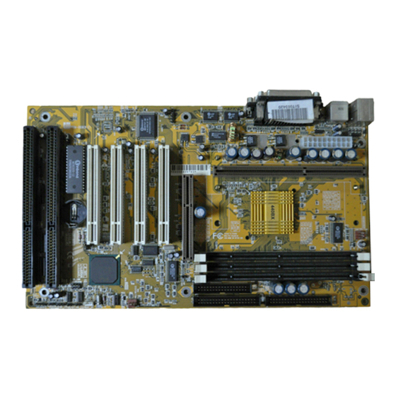
CHAPTER 1 INTRODUCTION Preface The motherboard is a 4 layer, ATX form factor high performance PCI/AGP mainboard. It includes Intel i82440BX system chipset, SMC FDC37M672 Super I/O controller. Features Processor • Intel Celeron, Pentium II/III • The mainboard can run with following speeds: 233-500MHz Chipset •... - Page 6 Chapter 1 System BIOS • Award/AMI BIOS (128KB Flash EPROM). Slots • One AGP slot • Four PCI slots (1 shared) • Three ISA slots(1 shared) Form Factor • Full ATX Size (305mm x 217mm) 4 Layer Fig. 1 Key Components of the Mainboard...
-
Page 7: Jumper Settings
CHAPTER 2 JUMPER SETTINGS JUMPERS PRESENTATION Pins 1 and 2 are shorted with a jumper cap. Pins 2 and 3 are shorted with a jumper cap. The jumper is shorted when the jumper cap is placed over the two pins of the jumper. The jumper is open when the jumper cap is removed from jumper. -
Page 8: Graphical Description Of Jumper Settings
Chapter 2 GRAPHICAL DESCRIPTION OF JUMPER SETTINGS Fig. 2 Jumper Location of the mainboard... -
Page 9: J3 - Cpu Clock Speed
Jumper Settings J3 - CPU CLOCK SPEED The table below summaries the Processor frequency and settings of each jumper of the motherboard. CPU Front Rating Setting (J3) Freq. Ratio Size Bus Freq. Pentium II 233MHz 66MHz 3.5x close open open close Pentium II 350MHz... -
Page 10: J4 - Clear Cmos Data
Chapter 2 J4 - CLEAR CMOS DATA J4 is used to clear the content of the CMOS Data in the RTC (build in PIIX4 chip). Table 3: Clear CMOS Data J6 - VOLTAGE SELECTION FOR SYSTEM ROM J6 is used to select the operation voltage of the system ROM. Table 4: Voltage Selection for System ROM... -
Page 11: Memory Configuartion
Jumper Settings MEMORY CONFIGUARTION When 100MHz Front Size Bus Processor is used. SDRAM DIMMs with PC/100 specification and Serial Presence Defect (SPD) data structure are required. The mainboard lets user upgrade system memory via DIMM sockets on the mainboard. On board memory is located in eight banks: Row 0 - 7. Four DIMM sockets are provided for 3.3V Synchronous DRAM. -
Page 12: Chapter 3 Connector Configuration
CHAPTER 3 CONNECTOR CONFIGURATION Once the mainboard has been fastened into system case, the next step is to connect the internal cables. The internal cables are wire leads with plastic female connectors that attach to the connectors. The mainboard connectors have varying numbers of pins and are the points of contact between the mainboard and other parts of the computer. -
Page 13: Connector Configuration
Connector Configuration JP1 - ATX POWER SUPPLY CONNECTOR Fig. 4 ATX Power Supply Connector JP10 - IrDA CONNECTOR JP10 is an IrDA connector that uses UART2 as interface of IrDA Infrared and HP SIR. Fig. 5 IrDA Connector JP12 - FLOPPY DRIVE CONTROLLER This connector supports the floppy drive ribbon cable. -
Page 14: Jp13 - Sb Link Connector
Chapter 3 JP13 – SB LINK CONNECTOR In order to migrate the legacy Sound Blaster compatible audio to the PCI bus, some Audio Card may incorporate a pair of PC/PCI request/grant sideband signals to interface to the PCI bus. This connector is provided for Creative PCI sound cards SB Link connection. -
Page 15: Jp18 - Speaker
Connector Configuration JP18 - SPEAKER JP18 is a four pins connector, which is used to connect the system speaker. Fig. 9 Speaker JP19 - POWER ON/OFF SWITCH It is used to switch on or off the ATX power supply. The power is turned on by short the power switch once. -
Page 16: Cpu Fan, System Fan & Chassis Fan Connector
Chapter 3 3.12 CPU FAN, SYSTEM FAN & CHASSIS FAN CONNECTOR These FAN connectors are used to connect with the CPU Fan or the Chassis Fan Power cable. Fig. 11 FAN Connector Fig. 12 I/O Connector 3.13 PS/2 KEYBOARD CONNECTOR This connector is a six-pin female mini DIN connector using a PS/2 plug. -
Page 17: Universal Serial Bus Port 0
Connector Configuration 3.15 UNIVERSAL SERIAL BUS PORT 0 & 1 These connectors are two four pin female sockets which are available for connecting USB device. 3.16 SERIAL PORT COM1 & COM2 This is a D-Type 9 pin male connector for pointing devices or other serial devices. 3.17 PARALLEL PORT CONNECTOR This is a D-Type 25 pin female connector. - Page 18 Chapter 3 Retention Mechanism Attach Mount Fig. 14 Before the installation of RM Kits find the six holes on the motherboard for RM installation. The hole position and usage is as following: Fig. 15 Installation Guide Mount the two RM Attach Mounts onto the motherboard from bottom side. These mounts will be used to attach the RM Assembly.
- Page 19 Connector Configuration Please refer to the diagram for the installation of Pentium II CPU Fig. 16a Please refer to the diagram for the installation of Celeron CPU or Pentium II in SECC2 package. Fig. 16b...
-
Page 20: Optional Heatsink Support Installation Guide
Chapter 3 3.19 OPTIONAL HEATSINK SUPPORT INSTALLATION GUIDE Optional Heatsink Support includes following components: Heatsink Top Support Fig. 17 Heatsink Support Base Fig. 18... - Page 21 Connector Configuration Installation Guide Refer to Fig. 15 install the Heatsink Support Base onto the motherboard, insert the two plastic nail to the hole in the Heatsink Support Base as following diagram: Fig. 19a Insert the Heatsink Top Support to the Pentium II Heatsink and the Heatsink Support Base as the following diagram: Fig.
-
Page 22: Award Bios Setup Guide
CHAPTER 4 AWARD BIOS SETUP GUIDE This following manual is specially provided for the BIOS supported system. After the configuration of the mainboard, and have assembled the components, user can turn on the completed system. At this point, run the software setup to ensure that the system information is correct. - Page 23 Award BIOS Setup Guide Press the <DEL> key to enter the AWARD BIOS setup program and the following screen appears: ROM PCI/ISA BIOS (2A69KD19) CMOS SETUP UTILITY AWARD SOFTWARE, INC. STANDARD CMOS SETUP INTEGRATED PERIPHERALS BIOS FEATURES SETUP SUPERVISOR PASSWORD CHIPSET FEATURES SETUP USER PASSWORD POWER MANAGEMENT SETUP...
-
Page 24: Standard Cmos Setup
Chapter 4 STANDARD CMOS SETUP ROM PCI/ISA BIOS (2A69KD19) STANDARD CMOS SETUP AWARD SOFTWARE, INC. Date (mm:dd:yy) : Wed, May 21 1997 Time (hh:mm:ss) : 20 : 27 : 55 HARD DISKS TYPE SIZE CYLS HEAD PRECOMP LANDZ SECTOR MODE Primary Master : Auto AUTO... -
Page 25: Bios Features Setup
Award BIOS Setup Guide BIOS FEATURES SETUP ROM PCI/ISA BIOS (2A69KD19) BIOS FEATURES SETUP AWARD SOFTWARE, INC. Virus Warning : Disabled Video BIOS Shadow : Disabled Quick Power On Self Test : Disabled C8000-CBFFF Shadow : Disabled Boot Sequence : A,C,SCSI CC000-CFFFF Shadow : Disabled Swap Floppy Drive... - Page 26 Chapter 4 Boot Up NumLock Status: Choose On or Off. On puts numeric keypad in Num Lock mode at boot-up. Off puts numeric keypad in arrow key mode at boot-up. Boot Up System Speed: Choose High or Low. Set the CPU timing at Boot Up, the default is high.
-
Page 27: Chipset Features Setup
Award BIOS Setup Guide CHIPSET FEATURES SETUP The Advanced Chipset Setup option is used to change the values of the chipset registers. These registers control most of the system options in the computer. Note: Change these Settings only if user is familiar with the Chipset. ROM PCI/ISA BIOS (2A69KD19) CHIPSET FEATURES SETUP AWARD SOFTWARE, INC. - Page 28 Chapter 4 System/Video BIOS Cacheable: Choose Enabled or Disabled. “Enabled” allows system/video BIOS be cacheable. Video RAM Cacheable: Choose Enabled or Disabled. “Enabled” allows video RAM to be cacheable. 8 Bit I/O Recovery Time: This item is used to set the recovery time allowed for 8 bit I/O access. Choices are from NA, 1 to 8 CPU clocks.
-
Page 29: Power Management Setup Menu
Award BIOS Setup Guide POWER MANAGEMENT SETUP MENU The Power Management Setup option is used to change the values of the chipset registers for system power management functions. ROM PCI/ISA BIOS (2A69KD19) POWER MANAGEMENT SETUP AWARD SOFTWARE, INC. Power Management : User Define ** Reload Global Timer Events ** PM Control by APM... - Page 30 Chapter 4 Video Off Method: Choose V/H SYNC+Blank, DPMS or Blank Screen. This is monitor Power Saving Method. V/H SYNC+Blank means turn off Vertical, Horizontal scanning and blank the screen. Blank Screen will blank the display screen. DPMS (Display Power Management System) can allow the System BIOS control the Display Card to turn off the Display.
-
Page 31: Pci Configuration
Award BIOS Setup Guide Reload Global Timer Event: When Enabled, an event occurring on each device listed below restarts the global time for Standby Mode. IRQ[3-7,9-15], NMI Primary IDE 0 Primary IDE 1 Secondary IDE 0 Secondary IDE 1 Floppy Disk Serial Port Parallel Port PCI CONFIGURATION... - Page 32 Chapter 4 A short description of the screen items follows: PNP OS Installed: Set this option to Yes if the operating system installed in the computer is Plug and Play-aware (e.g. Windows 95). Resources Controlled By: The Award Plug and Play BIOS can automatically configure all the boot and Plug and Play compatible device.
-
Page 33: Integrated Peripherals Setup Menu
Award BIOS Setup Guide INTEGRATED PERIPHERALS SETUP MENU The Integrated Peripherals setup option is need to change the values of the I/O chipset registers for I/O functions. ROM PCI/ISA BIOS (2A69KD19) INTEGRATED PERIPHERALS AWARD SOFTWARE, INC. IDE HDD Block Mode : Enabled Onboard Parallel Port : 3BC/IRQ7... - Page 34 Chapter 4 IDE Primary Master UDMA/IDE Primary Slave UDMA/IDE Secondary Master UDMA/IDE Secondary Slave UDMA: Available selection are “Auto” or “Disabled”. To choose “Auto”, the system BIOS will scan the IDE device to support Ultra DMA or not. On-Chip Primary/Secondary PCI IDE: This item is used to set the onboard IDE controller. The settings are Primary, Secondary, Both or Disabled.
-
Page 35: Load Setup Defaults Menu
Award BIOS Setup Guide LOAD SETUP DEFAULTS MENU This Main Menu item uses the default setup values. Use this option as a diagnostic aid if the system behaves erratically. Choose this item and the following message appears: “Load SETUP Defaults (Y/N)? N” To use the Power-On defaults, change the prompt to “Y”... -
Page 36: Ide Hdd Auto Detection
Chapter 4 4.11 IDE HDD AUTO DETECTION When users can not find the Hard Disk information, it is very helpful to use this option. Choose this item and press <Enter>. After couple seconds, the screen will appear the Hard Disk information and following message: “SELECT PRIMARY MASTER OPTION(N=SKIP): N”... -
Page 37: Chapter 5 Flash And Dmi Utility
CHAPTER 5 FLASH AND DMI UTILITY AWARD FLASH UTILITY This section will provide instructions to guide you through updating your old BIOS. The file name we use to program here is test.bin, and the file name to save old BIOS is 2A59F000.OLD. - Page 38 Chapter 5 If you do not wish to save the old BIOS: Please type “N”, and then press the ENTER key. Then you will be request to answer: “Are You Sure to Program?” Answer “N” if you do not want to program, and then it will exit. To save the old BIOS: Please respond “Y”, and then press the ENTER key.
-
Page 39: Desktop Management Interface (Dmi) Overview
Flash and DMI Utility DESKTOP MANAGEMENT INTERFACE (DMI) OVERVIEW This motherboard can support DMI within the BIOS level. DMI is able to auto- detect and record information pertinent to a computer’s system such as the CPU type, CPU speed, and internal/external frequencies, and memory size. The onboard BIOS will detect as many system information as possible and store those collected information in a 4KB block in the motherboard’s flash EPROM and allow the DMI to retrieve data from this database. - Page 40 Chapter 5 Use the ←→ (left-right) cursors to move the top menu items and the ↑↓ (up-down) cursor to move between the left hand menu items. The bottom of the screen will show the available keys for each screen. Press enter at the menu item to enter the right hand screen for editing. “Edit component”...
- Page 41 Flash and DMI Utility Load DMI File You can load the disk file to memory by entering a drive and path and file name here.
- Page 42 Chapter 5 Save DMI File You can save the DMI (normally only saved to flash ROM) to a file by entering the drive and path here. If you want to cancel save, you may press ESC and a message “Bad File Name” appears here to show it was not saved.
-
Page 43: Appendix Aquick Guide
APPENDIX A QUICK GUIDE The table below summaries the functions and settings of each jumper of the motherboard. Function Jumper Settings CPU Speed Pentium II 233, 350MHz 1-2 close 3-4 open Selection 5-6 open 7-8 close Celeron 266MHz, Pentium II 400MHz 1-2 close 3-4 close 5-6 close...
Need help?
Do you have a question about the PRM-0080I and is the answer not in the manual?
Questions and answers