
Subscribe to Our Youtube Channel
Related Manuals for DTK PAM-0057I


Summary of Contents for DTK PAM-0057I
- Page 1 PAM-0057I High Performance Pentium PCI Mainboard User’s Guide Edition 3.04 © 1998 DTK Computer, Inc. P/N: 155100-8624...
- Page 3 CAUTION The motherboard is an electrostatic sensitive device. Don’t open or handle except at a static-free workstation. Windows, MS-DOS, and MS Word are trademarks of Microsoft Corporation. Novell, Netware are trademarks of Novell, Inc. Lotus, 1-2-3, and Symphony are trademarks of Lotus Development Corporation. PC, AT, PC-DOS, OS/2 and Presentation Manager are trademarks of IBM Corporation.
-
Page 4: Table Of Contents
CONTENTS CHAPTER 1 INTRODUCTION CHAPTER 2 JUMPER SETTINGS JUMPERS PRESENTATION CPU TYPE 2.2.1 INTEL PENTIUM CPU 2.2.2 INTEL PENTIUM w/ MMX™ TECH (P55C) CPU 2.2.3 AMD-K6 CPU 2.2.4 AMD-K5 CPU 2.2.5 CYRIX 6x86 CPU 2.2.6 CYRIX 6x86L CPU 2.2.7 CYRIX 6x86MX CPU 2.2.8 IDT WinCHIP C6 CPU GRAPHICAL DESCRIPTION OF JUMPER SETTINGS... - Page 5 INTEGRATED PERIPHERALS SETUP MENU LOAD SETUP DEFAULTS MENU SUPERVISOR PASSWORD 4.10 USER PASSWORD 4.11 IDE HDD AUTO DETECTION 4.12 SCSI HARD DISK INSTALLATION 4.13 SAVE & EXIT SETUP MENU 4.14 EXIT WITHOUT SAVING MENU CHAPTER 5 FLASH AND DMI UTILITY AWARD FLASH UTILITY DESKTOP MANAGEMENT INTERFACE (DMI) OVERVIEW APPENDIX A...
-
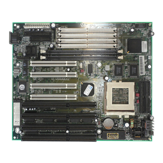
Page 7: Chapter 1 Introduction
CHAPTER 1 INTRODUCTION Preface The motherboard is a 4-layer, 2/3 baby AT size high-performance mainboard. It includes Intel 82430TX system chipset, Winbond W83877F/W83877TF Super I/O controller. Features Processor • Intel Pentium P54C, P55C series. • Cyrix 6x86, Cyrix 6x86L; AMD-K5 and AMD-K6 series 64-bit microprocessors. •... - Page 8 Chapter 1 Fig. 1 Key Components of the Mainboard...
-
Page 9: Power Specifications
Introduction PCI IDE • On board supports PCI Master IDE Controller, two connectors support up to four IDE devices such as HDD, CD ROM drive and Tape Back-up drives, etc. • PCI Master IDE controller supports PIO Mode 3 and 4 devices, I/O data transfer rate can be up to 17Mb/s. - Page 10 Chapter 1...
-
Page 11: Jumper Settings
CHAPTER 2 JUMPER SETTINGS JUMPERS PRESENTATION Pins 1 and 2 are shorted with a jumper cap. 1 2 3 Pins 2 and 3 are shorted with a jumper cap. 1 2 3 The jumper is shorted when the jumper cap is placed over the two pins of the jumper. -
Page 12: Intel Pentium W/ Mmx™ Tech (P55C) Cpu
Chapter 2 2.2.2 INTEL PENTIUM w/ MMX™ ™ TECH (P55C) CPU The Intel Pentium w/ MMX™ Tech (P55C) CPU is offered with dual voltage supply - 2.8V for core and 3.3V (I/O) interface. The following is the marking for identify the CPU type. -
Page 13: Amd-K5 Cpu
Jumper Settings 2.2.4 AMD-K5 CPU The AMD-K5 family CPU operates on different operation voltage depending on the CPU type. The operating voltage can be known through the marking on the surface of the CPU. (The following diagram is provided as an example only. It does not necessarily indicate a valid product marking.) Fig. -
Page 14: Cyrix 6X86L Cpu
Chapter 2 2.2.6 CYRIX 6x86L CPU The Cyrix 6x86L has different I/O and core voltage. Please refer to the CPU marking. Fig. 2f CPU Description (Top Side) 2.2.7 CYRIX 6x86MX CPU The Cyrix 6x86MX has different I/O and Core Voltage. Please refer to the CPU marking. -
Page 15: Idt Winchip C6 Cpu
Jumper Settings 2.2.8 IDT WinCHIP C6 CPU The IDT WinChip C6 CPU has different operation voltage. Please refer to the CPU marking to identify the operating voltage. Fig. 2h CPU Description... -
Page 16: Graphical Description Of Jumper Settings
Chapter 2 GRAPHICAL DESCRIPTION OF JUMPER SETTINGS Fig. 3 Jumper Location... -
Page 17: Cpu Voltage Selection
Jumper Settings CPU VOLTAGE SELECTION 3.3V Single Voltage CPU: P54C, P54CT, 3.3 IDT WinChip C6 Fig. 4a CPU Type - 3.3V 3.5V Single Voltage CPU: P54C-VRE, AMD-K5, Cyrix 6x86, 3.5V IDT WinChip C6 Fig. 4b CPU Type - 3.5V... - Page 18 Chapter 2 3.3V (I/O)/2.2V (core) Dual Voltage CPU: 2.2V AMD-K6 and AMD-K6-2 Fig. 4c CPU Type – 3.3V/2.2V 3.3V (I/O)/2.8V (core) Dual Voltage CPU: P55C, Cyrix 6x86L Fig. 4d CPU Type - 3.3V/2.8V...
- Page 19 Jumper Settings 3.3V (I/O)/2.9V (core) Dual Voltage CPU: 2.9V AMD-K6, Cyrix 6x86MX and Cyrix M II Fig. 4e CPU Type - 3.3V/2.9V 3.3V (I/O)/3.2V (core) Dual Voltage CPU: 3.2V AMD-K6/233 Fig. 4f CPU Type - 3.3V/3.2V...
-
Page 20: Cpu To Bus Frequency Ratio (Jp12)
Chapter 2 CPU TO BUS FREQUENCY RATIO (JP12) JP12 set the frequency ration between the Internal frequency of the CPU and the External frequency (called the Bus clock) within the CPU. These must be set together with the below jumpers CPU External (Bus) Frequency Selection. CPU EXTERNAL (BUS) FREQUENCY SELECTION (JP9, JP10, JP13) JP9, JP10, JP13 tell the clock generator what frequency to send to the CPU. - Page 21 Jumper Settings Bus Freq. Setting CPU Type Freq. Ratio Ratio Setting (JP12) Freq. JP10 JP13 AMD-K6/166 166MHz 2.5x 66MHz open open Cyrix M II-300 233MHz 3.5x 66MHz open open Cyrix M II-300 225MHz 3.0x 75MHz open close Cyrix 6x86MX-PR233 200MHz 3.0x 66MHz open open...
-
Page 22: Memory Configuration
Chapter 2 MEMORY CONFIGURATION The Mainboard lets user upgrade system memory via SIMM sockets and DIMM sockets on the mainboard. Four SIMM sockets (SIMM1, SIMM2, SIMM3, SIMM4) are provided for SPM, FPM and EDO RAM SIMM and two DIMM sockets (DIMM1, DIMM2) are available for the SDRAM or 3.3V EDO DIMM. -
Page 23: Cache Memory Configuration
Jumper Settings Double means Double side SIMM Module or Double side DIMM Module. The size of Double side SIMM can be 8MB, 32MB and the size of Double side DIMM can be 16MB, 64MB. **Note: based on above chart, the different types of SIMM can be in different bank, but within same bank, the two SIMM modules must be of same type and size. - Page 24 Chapter 2...
-
Page 25: Connectors Configuration
CHAPTER 3 CONNECTORS CONFIGURATION Once the mainboard has been fastened into system case, the next step is to connect the internal cables and external cables. The mainboard connectors have varying numbers of pins and are the points of contact between the mainboard and other parts of the computer. Fig. -
Page 26: J2 - Reset Switch, Smi Switch, Speaker, Turbo Led, Keylock And Hdd Led Connector
Chapter 3 J2 - RESET SWITCH, SMI SWITCH, SPEAKER, TURBO LED, KEYLOCK AND HDD LED CONNECTOR J2 is a 2x10 pin header for Hard Disk LED, Keyboard Lock, Turbo LED, Suspense Switch, Reset Switch and Speaker Connector. Fig. 7 • RESET SWITCH CONNECTOR Attach the Reset switch cable to this connector. - Page 27 Connector Configuration • SPEAKER CONNECTOR Fig. 8 Speaker Connector • TURBO LED CONNECTOR Turbo LED on front of the system case. If the system board select is in Turbo mode, the indicator lights during high-speed operation. This motherboard always operate at high-speed. Fig.
-
Page 28: J10 - Primary Ide Connector
Chapter 3 • KEYLOCK CONNECTOR Close this jumper will disable the keyboard. Fig. 10 Keylock Connector • HDD LED CONNECTOR Connected this jumper to the HDD LED on front of the system case. If the HDD is in operation, the indicator lights during operation. Fig. -
Page 29: J11 - Secondary Ide Connector
Connector Configuration J11 - SECONDARY IDE CONNECTOR J11 locates above the J10, the primary IDE connector with pin 1 on the left. J12 - USB0, USB1, PS/2 MOUSE EXTENSION, IrDA AND FAST IR CONNECTOR J12 is a 2x10 pin header for USB0, USB1, PS/2 mouse extension, IrDA and Fast IR connector, and it is also designed as the connector for the optional USB extension card. -
Page 30: J13 - Serial Port
Chapter 3 J13 - SERIAL PORT 2 J13 is left to J14. Pin 1 is on the right. J14 - SERIAL PORT 1 Both COM1 and 2 are 16550 fast UART compatible. J14 is located right of J15 Parallel Connector. Pin 1 is on the right. J15 - PARALLEL PORT J15 is up to DRAM SIMM Module connector. -
Page 31: J20 - Keyboard Connector
Connector Configuration 3.10 J20 - KEYBOARD CONNECTOR A standard five-pin female DIM keyboard connector is located at the rear of the keyboard. Plug the jack on the keyboard cable into this connector. Fig. 14 J20 Keyboard Connector 3.11 J21 - PS/2 STYLE KEYBOARD CONNECTOR (OPTIONAL) A PS/2 Standard six-pin female DIM connector for keyboard is located at right to J20. -
Page 32: J22 - Power Supply Connector
Chapter 3 3.12 J22 - POWER SUPPLY CONNECTOR The power supply connector has two six-pin male header connectors. Plug the dual connectors from the power directly onto the board connector. Description Power Good (Orange) +5 VDC (Red) +12 VDC (Yellow) -12 VDC (Blue) Ground (Black) Ground (Black) -
Page 33: Award Bios Setup Guide
CHAPTER 4 AWARD BIOS SETUP GUIDE This following manual is specially provided for the BIOS supported system. After the configuration of the mainboard, and have assembled the components, user can turn on the completed system. At this point, run the software setup to ensure that the system information is correct. - Page 34 Chapter 4 Press the <DEL> key to enter the AWARD BIOS setup program and the following screen appears: ROM PCI/ISA BIOS (2A59ID19) CMOS SETUP UTILITY AWARD SOFTWARE, INC. STANDARD CMOS SETUP INTEGRATED PERIPHERALS BIOS FEATURES SETUP SUPERVISOR PASSWORD CHIPSET FEATURES SETUP USER PASSWORD POWER MANAGEMENT SETUP IDE HDD AUTO DETECTION...
-
Page 35: Standard Cmos Setup
STANDARD CMOS SETUP ROM PCI/ISA BIOS (2A59ID19) STANDARD CMOS SETUP AWARD SOFTWARE, INC. Date (mm:dd:yy) : Mon, Feb 03 1997 Time (hh:mm:ss) : 15 : 23 : 15 HARD DISKS TYPE SIZE CYLS HEAD PRECOMP LANDZ SECTOR MODE Primary Master : Auto AUTO Primary Slave None... -
Page 36: Bios Features Setup
Chapter 4 BIOS FEATURES SETUP ROM PCI/ISA BIOS (2A59ID19) BIOS FEATURES SETUP AWARD SOFTWARE, INC. Virus Warning : Disabled Video BIOS Shadow : Enabled CPU Internal Cache : Enabled C8000-CBFFF Shadow : Disabled External Cache : Enabled CC000-CFFFF Shadow : Disabled Quick Power On Self Test : Disabled D0000-D3FFF Shadow... - Page 37 Swap Floppy Drive: Choose Enabled or Disabled. This option lets end users to change the Drive A: or B: to others. Boot Up Floppy Seek: Choose Enabled or Disabled. "Disabled" provides a fast boot and reduces the possibility of damage to the heads. Boot Up NumLock Status: Choose On or Off.
-
Page 38: Chipset Features Setup
Chapter 4 CHIPSET FEATURES SETUP The Advanced Chipset Setup option is used to change the values of the chipset registers. These registers control most of the system options in the computer. Note: Change these Settings only if user is familiar with the Chipset. ROM PCI/ISA BIOS (2A59ID19) CHIPSET FEATURES SETUP AWARD SOFTWARE, INC. -
Page 39: Power Management Setup Menu
8 Bit I/O Recovery Time: This item allows you to determine the recovery time allowed for 8 bit I/O. Choices are from NA, 1 to 8 CPU clocks. 1 clock is the default. 16 Bit I/O Recovery Time: This item allows you to determine the recovery time allowed for 16 bit I/O. - Page 40 Chapter 4 A short description of the screen items follows: ACPI Function: To enable feature for supporting the operating system with Advanced Configuration and Power Interface. (such as Windows 98) Power Management: Available selection are “Disabled”, “User Define”, “Max Saving” and “Min Saving”: “Disabled”...
-
Page 41: Pnp/Pci Configuration
PnP/PCI CONFIGURATION The PCI Configuration Setup option is used to configure the PCI add-on Cards on PCI Slots. Without proper setup the PCI Add-on Cards might not function properly. ROM PCI/ISA BIOS (2A59ID19) PNP/PCI CONFIGURATION AWARD SOFTWARE, INC. PNP OS Installed : Yes PCI IDE IRQ Map To : PCI-AUTO... -
Page 42: Integrated Peripherals Setup Menu
Chapter 4 PCI IRQ Active By: Choose Level or Edge. The default settings is Level. PCI IDE IRQ Map To: Choose PCI-AUTO, PCI-SLOT1, PCI-SLOT2, PCI-SLOT3, ISA. The default setting is PCI-AUTO. Used MEM Base Addr/Used MEM Length: These items will be shown only when “Resources Controlled By”... - Page 43 A short description of the screen items follows: IDE HDD Block Mode: This allows your hard controller to use the fast block mode to transfer data to and from your hard disk drive (HDD). Enabled is the default. IDE PIO: PIO means Programmed Input/Output. Rather than have the BIOS issue a series of commands to effect a transfer to or from the disk drive, PIO allows the BIOS to tell the controller what it wants and then let the controller and the CPU perform the complete task by themselves.
-
Page 44: Load Setup Defaults Menu
Chapter 4 Onboard Parallel Port: Choose None or with four different I/O Address and corresponding IRQx. While choosing proper I/O Address, be sure not to cause Address conflict with other I/O devices. Onboard Parallel Mode: Choose SPP, EPP/SPP, ECP, ECP/EPP Mode. Make proper selection with the attached printer port device. -
Page 45: User Password
4.10 USER PASSWORD With the user password, only booting up the system is accepted, but changing the BIOS setup is not allowed. 4.11 IDE HDD AUTO DETECTION When users can not find the Hard Disk information, it is very helpful to use this option. Choose this item and press <Enter>. -
Page 46: Exit Without Saving Menu
Chapter 4 4.14 EXIT WITHOUT SAVING MENU When you select this function, the following message will appear at the centre of the screen to assist you to Abandon all Data and Exit Setup. Quit Without Saving (Y/N)? -
Page 47: Flash And Dmi Utility
CHAPTER 5 FLASH AND DMI UTILITY AWARD FLASH UTILITY This section will provide instructions to guide you through updating your old BIOS. The file name we use to program here is test.bin, and the file name to save old BIOS is 2A59F000.OLD. - Page 48 Chapter 5 If you do not wish to save the old BIOS: Please type “N”, and then press the ENTER key. Then you will be request to answer: “Are You Sure to Program?” Answer “N” if you do not want to program, and then it will exit. To save the old BIOS: Please respond “Y”, and then press the ENTER key.
-
Page 49: Desktop Management Interface (Dmi) Overview
Chapter 5 DESKTOP MANAGEMENT INTERFACE (DMI) OVERVIEW This motherboard can support DMI within the BIOS level. DMI is able to auto- detect and record information pertinent to a computer’s system such as the CPU type, CPU speed, and internal/external frequencies, and memory size. The onboard BIOS will detect as many system information as possible and store those collected information in a 4KB block in the motherboard’s flash EPROM and allow the DMI to retrieve data from this database. - Page 50 Chapter 5 Use the ←→ (left-right) cursors to move the top menu items and the ↑↓ (up-down) cursor to move between the left hand menu items. The bottom of the screen will show the available keys for each screen. Press enter at the menu item to enter the right hand screen for editing. “Edit component”...
- Page 51 Chapter 5 Load DMI File You can load the disk file to memory by entering a drive and path and file name here.
- Page 52 Chapter 5 Save DMI File You can save the DMI (normally only saved to flash ROM) to a file by entering the drive and path here. If you want to cancel save, you may press ESC and a message “Bad File Name” appears here to show it was not saved.
-
Page 53: Quick Guide
APPENDIX A QUICK GUIDE The table below summaries the functions and settings of each jumpers of the motherboard. Function Jumper Settings 3.3V Single Voltage CPU: JP1: short JP7: A-B open For P54C, P54CT, 3.3V IDT WinChip C6 JP5: short 1-2 short Voltage Selection 3-4 short... - Page 54 Appendix A Function Jumper Settings For 150MHz Intel Pentium and JP9: 2-3 short JP12: 1-2 short CPU Speed Cyrix 6x86MX-PR166 CPU JP10: 2-3 short 3-4 open Selection JP13: 1-2 short For 150MHz Cyrix 6x86L/MX-PR200 CPU JP9: 2-3 short JP12: 1-2 open JP10: 1-2 short 3-4 short...
- Page 55 Quick Guide...
- Page 56 Appendix A...
Need help?
Do you have a question about the PAM-0057I and is the answer not in the manual?
Questions and answers