Table of Contents
Advertisement
Quick Links
Features
The AT697F evaluation board provides the following features:
On-board power supply circuitry
for external power supply sources connection
for board powering by the CPCI interface
On-board reset
On-board memories
FLASH (40-bit capability)
SRAM (40-bit SRAM capability)
SDRAM (40-bit SDRAM capability)
Status indicators
Power
Processor Error + Run
DSU activity
Clock circuitry
On board oscillator for clock generator
External clock source connection
RS232 hardware connector dedicated to the Debug Support Unit (DSU)
RS232 hardware connector dedicated to a universal UART
PCI interface
Host / Satellite capability
User defined push-buttons
User defined LEDs
Expansion connector
10-pin JTAG interface connector
Description
The AT697F Evaluation Kit is a development system for the ATMEL AT697F, 32-bit
SPARC® V8 processor based on LEON2 fault tolerant model.
The kit is equipped with a rich set of peripherals that make the AT697F Evaluation Kit
perfect evaluation platform to quickly and easily develop application on the AT697F
processor. This guide shows the user how to quickly get started with this kit.
APPLICATION NOTE
AT697F Evaluation Kit
USER GUIDE
7540HAERO10/15
Advertisement
Table of Contents

Subscribe to Our Youtube Channel
Related Manuals for Atmel AT697F


Summary of Contents for Atmel AT697F
- Page 1 The AT697F Evaluation Kit is a development system for the ATMEL AT697F, 32-bit SPARC® V8 processor based on LEON2 fault tolerant model. The kit is equipped with a rich set of peripherals that make the AT697F Evaluation Kit perfect evaluation platform to quickly and easily develop application on the AT697F processor.
-
Page 2: Table Of Contents
2.15 Expansion connector ..................27 2.16 Mechanical drawing ..................29 2.17 Board History ....................30 3. Appendix A – Getting Started ............31 AT697 Development Kit Content ..............31 Handling ......................32 System requirements ..................32 Evaluation Kit AT697F V3.0 [APPLICATION NOTE]... - Page 3 Default switches configuration: ............33 3.5.2 Power supply setup:................33 3.5.3 Serial communication link: ..............33 3.5.4 GRMON: ................... 33 Run your first application ................. 34 4. Appendix B – Schematics ..............38 5. Revision History ................38 Evaluation Kit AT697F V3.0 [APPLICATION NOTE]...
-
Page 4: Overview
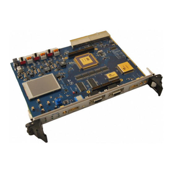
Overview Figure 1-1 AT697 Evaluation board v3.0 Scope The AT697F eveluation kit aims at protoyping easly applications running on an AT697F processor. This guide focuses on the description of the AT697F evlaluation kit. Deliverables The AT697F evaluation kit package contains the following items: ... -
Page 5: Features
Here is an overview of the main operational features embedded on the evaluation board: Table 1-1. AT697F V3.0 board features Characteristics Specifications AT697F, powered in 3.3V and 1.8V Board Power Supply Audio jack connector (3.5mm) 3x Terminal blocks (direct 5V, 3.3V and 1.8V) Compact-PCI powering 25MHz clock generator –... -
Page 6: Hardware Description
Hardware description Block diagram Figure 2-1 AT697F Evaluation board block diagram AT697F I-Cache Interger Unit (SPARC V8) D-Cache SDRAM Flash 8 Buffer bits Flash conf Flash JTAG Connector JTAG Memory 40 bits AMBA controller Controller RS232 serial link SRAM 40 bits... -
Page 7: Evaluation Board
SDRAM Expansion Expansion connector connector 1V8 direct power 1V8 source selection 3V3 direct power Power 3V3 source selection Supply HMI LEDs 5V direct power 5V source selection EXT power 8-12V LCD 240x320 HMI Buttons Evaluation Kit AT697F V3.0 [APPLICATION NOTE]... -
Page 8: Manufacturing Configuration
SW37.4 SKEW 1 configuration SW37.5 Connect the processor watchdog to the RESET device SW37.6 Select the processor clock. SW37.7 This switch will select the PROM width. SW37.8 Select PIO3 signal. SW37.9 N.C. SW37.10 N.C. Evaluation Kit AT697F V3.0 [APPLICATION NOTE]... -
Page 9: Board Power Supply
Important: when the board is powered from the CPCI connector, switch for 3.3V and 5V shall be placed in “ext position” whereas switch 1.8V shall be keep in “reg position”. Do not connect any power supply except the one coming from CPCI connector. Evaluation Kit AT697F V3.0 [APPLICATION NOTE]... -
Page 10: Processor
Processor 2.5.1 Processor Package On the evaluation kit, the AT697 32-bit SPARC processor is embedded. The processor package is the MQFP-256 space qualified package. Figure 2-6 MQFP-256 package 2.5.2 Processor Pin-out Evaluation Kit AT697F V3.0 [APPLICATION NOTE]... - Page 11 Evaluation Kit AT697F V3.0 [APPLICATION NOTE]...
- Page 12 Evaluation Kit AT697F V3.0 [APPLICATION NOTE]...
-
Page 13: Memories
2.6.2.1 PROM Overview The AT697F is able to work with two bus widths: 8 bits or 32 bits. In both cases, the processor can use the EDAC mode. If EDAC is enabled on the PROM 40, the processor needs 8 more bits. -
Page 14: Prom40 Configuration (Sw37.7 Is Off)
The 8-bit boot PROM is based on three M29W800D Flash memories (U22). The chip is directly soldered on the board. PROM8 is implemented on the bottom side of the board close to the PROM40. IMPORTANT: when EDAC is activated with PROM8, memory available is less than without EDAC. Evaluation Kit AT697F V3.0 [APPLICATION NOTE]... -
Page 15: Prom Expansion
Because of an inversion of write enable signals WE[3:0], the processor can’t use SRAM in 8 bits mode without a patch. Since V3.0.2 a modification has been is done to allow the processor the use SRAM in 8 bits mode. Following picture illustrate the fixe in the schematic (p36): Evaluation Kit AT697F V3.0 [APPLICATION NOTE]... -
Page 16: Sdram Configuration
1x SDRAM 16 bits (only 8 bits are used) for the checkbit (EDAC protection): MT48LC16M16A2P-6A (U27) This provides an access to 256MBits of SDRAM data/code Figure 2-10. SDRAM implementation Top side Bottom side 1: SDRAM for data 2: SDRAM for EDAC Evaluation Kit AT697F V3.0 [APPLICATION NOTE]... -
Page 17: Board Hmi
(1): To use this function, SW37.8 must be OFF. 2.7.2 Board LEDs LEDs are driven by a NPN transistor. A hight level on a PIO put the LED on. Figure 2-13. LEDs implantation Table 2-4 LEDs mapping Evaluation Kit AT697F V3.0 [APPLICATION NOTE]... -
Page 18: Board Display
Table 2-6 UART 1 mapping Serial link name Function Processor connexion UART1_RX Serial link receive data PIO 14 UART1_TX Serial link transmit data PIO 15 UART1_RTS Request to Send frame N.C. UART1_CTS Clear to Send frame N.C. Evaluation Kit AT697F V3.0 [APPLICATION NOTE]... -
Page 19: Serial Link 2
The PCI interface has been designed to be integrated in compact PCI back plane. Universal keying is implemented. The board form factor fits with the 6U standard. The HOST/SATELLITE mode is automatically configured through position of the board on the PCI rack. Evaluation Kit AT697F V3.0 [APPLICATION NOTE]... -
Page 20: Clock Management
Clock PLL configuration interface CLK EXT 1 UART Control Reg. connector UACn Clock configuration 25 MHz Clock SPP Connector UART RS232 serial link generator 33 MHz interface connector interface Legend: Configuration switch Connector Evaluation Kit AT697F V3.0 [APPLICATION NOTE]... -
Page 21: Internal Clocks
OFF: processor use on-board 25MHz clock 180 / P15 ON: processor use Clock EXT IN 1 UART CLK OFF: PIO3 is connected to Press Button ENTER 63 / F4 ON: PIO3 is connected to Clock EXT IN 2 Evaluation Kit AT697F V3.0 [APPLICATION NOTE]... -
Page 22: Evaluation Kit Reset
An integrated circuit measures PWR_5V, PWR_3V3 and PWR_1V8 signals on the board. If these voltages are out of range (+/- 10% nominal value), the circuit reset the board or keep the board under reset (during a power on for example). Evaluation Kit AT697F V3.0 [APPLICATION NOTE]... -
Page 23: Space Programmer (Spp) Reset
RS232 communication and the debug facilities. The debug connector is available on front panel. It’s named “DSU connector”. Figure 2-17. DSU implementation DSUBRE press button DSUACT DEL DSU Connector Evaluation Kit AT697F V3.0 [APPLICATION NOTE]... -
Page 24: Jtag Connector
VCC3V3 TDI Test Points 2.14 2.14.1 Current measurement test points Current measurement test points are arranged according to the following drawing: Figure 2-18. Current probe footprint 2.54mm 2.54mm 2.54mm R shunt 0.01R B, C Evaluation Kit AT697F V3.0 [APPLICATION NOTE]... -
Page 25: Clocks Test Points
Figure 2-19. Power test points TP_I_1V8 TP_I_1V8_PLL TP_DEVICE_1V8 TP_BOARD _1V8 TP_ DEVICE _3V3 TP_BOARD_3V3 TP_BOARD_5V 2.14.2 Clocks test points Figure 2-20. Clock test points CLK ext 2 CLK ext 1 25 MHz 33 MHz Processor clock input SDCLK Evaluation Kit AT697F V3.0 [APPLICATION NOTE]... -
Page 26: System And Cpci Test Points
2.14.3 System and CPCI test points Figure 2-21. System and CPCI test points PCI clock PCI reset BEXC Processor error Board reset Evaluation Kit AT697F V3.0 [APPLICATION NOTE]... -
Page 27: Expansion Connector
N.C. PCI_AD6 PCI_AREQ2 N.C. N.C. N.C. PCI_AD5 PCI_AREQ3 N.C. N.C. N.C. PCI_AD4 PCI_AGNT0 N.C. N.C. N.C. PCI_AD3 PCI_AGNT1 N.C. N.C. N.C. PCI_AD2 PCI_AGNT2 N.C. N.C. N.C. PCI_AD1 PCI_AGNT3 N.C. N.C. N.C. PCI_AD0 N.C. N.C. Evaluation Kit AT697F V3.0 [APPLICATION NOTE]... - Page 28 RWE0 HMI_LED0 BOARD_5V DSUBRE RWE1 HMI_LED1 BOARD_5V TRST RWE2 HMI_LED2 PROC_CLK_SEL RWE3 HMI_LED10 PROM_WIDHT_SEL SDCLK BEXC UART_CLK_SEL SDRAS BRDY ALTERNATE_RESET SDCAS SDWE HMI_PB10 SDDQM0 HMI_PB4 SDDQM1 HMI_PB3 SDDQM2 HMI_PB2 SDDQM3 HMI_PB1 SDCS0 HMI_PB0 SDCS1 Evaluation Kit AT697F V3.0 [APPLICATION NOTE]...
-
Page 29: Mechanical Drawing
Mechanical drawing 2.16 Figure 2-22. PCB mechanical drawing 5.97 233.35 106.7 160 mm Evaluation Kit AT697F V3.0 [APPLICATION NOTE]... -
Page 30: Board History
Board History 2.17 Table 2-12 Board history Version Comments AT697F Evaluation Kit V3.0.1 First release. Change U23 to a TPS386040RGP AT697F Evaluation Kit V3.0.2 Add manual fixes to have access to SRAM8 from the processor Evaluation Kit AT697F V3.0 [APPLICATION NOTE]... -
Page 31: Appendix A - Getting Started
Notes: 1. only for Development kit. Documentation – AT697 Evaluation Kit User Manual – AT697 datasheet and erratasheet – BCC, RCC, and GRmon user manuals Application examples – General demonstration – PCI demonstration Evaluation Kit AT697F V3.0 [APPLICATION NOTE]... -
Page 32: Handling
GRMON - Debug monitor (only included in development kit) Installation procedure for each tool is specified in the corresponding User Guide. Please refer to the documents available with GRMON after installation for detailed information. Evaluation Kit AT697F V3.0 [APPLICATION NOTE]... -
Page 33: Hardware Setup
DSU connector (P1) and to one of the host platform RS232 connector. The host platform running GRMON under Linux or Windows environment is then used to establish the communication with the AT697 processor. Figure 4-1. Host Connection Evaluation Kit AT697F V3.0 [APPLICATION NOTE]... -
Page 34: Run Your First Application
Open a terminal window on your host platform in order to run GRmon (refer to GRmon user manual for details). under WINDOWS: "grmon -leon2 -uart COM1 -baud 115200" under LINUX: "grmon -leon2 -uart /dev/ttyS0 -baud 115200” where the "-uart" and "-baud" flags are to be set according to your communication interface configuration. Evaluation Kit AT697F V3.0 [APPLICATION NOTE]... - Page 35 "-uart" and "-baud" flags are to be set according to your communication interface configuration, and the “-romws” and “-ramws” flags are to be tuned with respect to the AT697F internal clock frequency. Other options can be added to the command line.
- Page 36 The executable can be loaded to RAM applying the following command: “load application” Step 5B: load to ROM: The ROM boot strap can be loaded to the on board flash applying the following commands: “flash enable” “flash erase all” “flash load rom_application” Evaluation Kit AT697F V3.0 [APPLICATION NOTE]...
- Page 37 Step 5A: execute code from RAM: To execute the loaded program, use “run” command. Step 5B: execute code from ROM: There are two ways to execute the code: Use “go 0” command under GRMON. Or restart the Evaluation Kit. Evaluation Kit AT697F V3.0 [APPLICATION NOTE]...
-
Page 38: Appendix B - Schematics
Please refer to the file in pdf format contained in the CD-ROM to see the Evaluation Kit schematic. Revision History Doc. Rev. Date Comments 7540F 02/2013 Initial document release 7540G 12/2014 Add fixes for SRAM8 access problem 7540H 10/2015 Change comments when using CPCI rack power supply Evaluation Kit AT697F V3.0 [APPLICATION NOTE]... - Page 39 Other terms and product names may be trademarks of others. Disclaimer: The information in this document is provided in connection with Atmel products. No license, express or implied, by estoppel or otherwise, to any intellectual property right is granted by this document or in connection with the sale of Atmel products.
Need help?
Do you have a question about the AT697F and is the answer not in the manual?
Questions and answers