Xilinx Virtex-6 FPGA Getting Started Manual
Connectivity kit
Hide thumbs
Also See for Virtex-6 FPGA:
- Manual (381 pages) ,
- User manual (317 pages) ,
- Getting started (72 pages)

Related Manuals for Xilinx Virtex-6 FPGA


Summary of Contents for Xilinx Virtex-6 FPGA
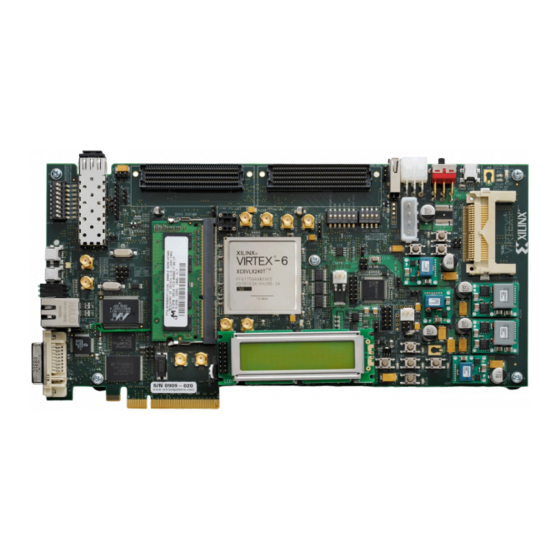
- Page 1 Virtex-6 FPGA Connectivity Kit Getting Started Guide UG664 (v1.4) July 6, 2011 XPN 0402826-03...
-
Page 2: Revision History
(including loss of data, profits, goodwill, or any type of loss or damage suffered as a result of any action brought by a third party) even if such damage or loss was reasonably foreseeable or Xilinx had been advised of the possibility of the same. - Page 3 Added Windows Driver. Added Linux Driver heading before step 1 page Updated step 2a and step 3a on page 56. Updated Table 1. Updated Figure 52 Figure Figure UG664 (v1.4) July 6, 2011 www.xilinx.com Virtex-6 FPGA Connectivity Kit Getting Started...
- Page 4 Virtex-6 FPGA Connectivity Kit Getting Started www.xilinx.com UG664 (v1.4) July 6, 2011...
-
Page 5: Table Of Contents
Modifications to the Connectivity TRD ........63 Getting Started with the Virtex-6 FPGA IBERT Reference Design . - Page 6 Virtex-6 FPGA Connectivity Kit Getting Started UG664 (v1.4) July 6, 2011...
-
Page 7: Preface: About This Guide
To search the Answer Database of silicon, software, and IP questions and answers, or to create a technical support WebCase, see the Xilinx website at: http://www.xilinx.com/support. Use this site for technical support regarding the installation and use of the product license file. - Page 8 Preface: About This Guide www.xilinx.com Virtex-6 FPGA Connectivity Kit Getting Started UG664 (v1.4) July 6, 2011...
-
Page 9: Virtex-6 Fpga Connectivity Kit
Note: The screen captures in this document are conceptual representatives of their subjects and provide general information only. For the latest information, see the Xilinx® ISE® Design Suite. Connectivity Kit Contents This section describes the kit deliverables provided in the box and indicates what can be found on the Xilinx website. -
Page 10: What Is Available Online
Figure 1) demonstrates the main integrated components in a Virtex-6 FPGA. The Integrated Endpoint Block for PCI Express and GTX transceivers work together in an application with additional IP cores, such as a Northwest Logic Packet DMA engine for the PCI Express interface, XAUI LogiCORE™ IP, and Memory controller IP generated using the Memory Interface Generator (MIG). - Page 11 Xilinx IP Third Party IP FPGA Logic UG664_01_092810 Figure 1: Block Diagram of the Virtex-6 FPGA Targeted Reference Design The Virtex-6 FPGA Connectivity TRD features these components: • Virtex-6 FPGA Integrated Block for PCI Express core configured as a 4-lane at 5 Gb/s or 8-lane at 2.5 Gb/s Endpoint for PCI Express, v2.0 •...
-
Page 12: Hardware Demonstration Setup Instructions
Hardware Demonstration Setup Instructions This section describes how to set up the hardware demonstration for the Virtex-6 FPGA Connectivity TRD. This demonstration outlines a bridging function between PCIe and XAUI protocols. It also provides accesses to an onboard DDR3 memory. - Page 13 X-Ref Target - Figure 2 Switch S2 Switch S1 UG664_02_022310 Figure 2: ML605 and FMC Connectivity Daughter Card X-Ref Target - Figure 3 CX4 Loopback Connector UG664_03_022310 Figure 3: CX4 Connector Virtex-6 FPGA Connectivity Kit Getting Started www.xilinx.com UG664 (v1.4) July 6, 2011...
- Page 14 After the hardware setup is complete, the user can choose to install the Windows driver or the Linux driver. Proceed to Install Linux Driver, page 27 to verify the design on the Fedora 10 operating system. www.xilinx.com Virtex-6 FPGA Connectivity Kit Getting Started UG664 (v1.4) July 6, 2011...
-
Page 15: Install Windows Driver
The system recognizes a new PCIe endpoint card connected to it and starts the Found New Hardware Wizard. Click on Cancel to close the wizard (Figure X-Ref Target - Figure 6 UG664_57_052011 Figure 6: Ignore Found New Hardware Wizard Virtex-6 FPGA Connectivity Kit Getting Started www.xilinx.com UG664 (v1.4) July 6, 2011... - Page 16 Install the drivers and GUI: Navigate to the v6_pcie_10Gdma_ddr3_xaui_axi folder. b. Double click on x_v6_trd_setup.exe (Figure X-Ref Target - Figure 7 UG664_58_060811 Figure 7: Run x_v6_trd_setup.exe www.xilinx.com Virtex-6 FPGA Connectivity Kit Getting Started UG664 (v1.4) July 6, 2011...
- Page 17 Getting Started with the Connectivity Targeted Reference Design Demo The InstallShield wizard for the Virtex-6 FPGA Connectivity TRD is launched (Figure 8). Click on Next to select the setup type. X-Ref Target - Figure 8 UG664_59_060811 Figure 8: InstallShield Wizard is Launched Virtex-6 FPGA Connectivity Kit Getting Started www.xilinx.com...
- Page 18 Click on Next and confirm the Setup Type selection (Figure X-Ref Target - Figure 9 UG664_60_060811 Figure 9: Set Directory to which the Driver Files are Copied www.xilinx.com Virtex-6 FPGA Connectivity Kit Getting Started UG664 (v1.4) July 6, 2011...
- Page 19 (Figure 10). At the end of this install process, the driver and GUI files are copied to the C:\Program Files\Xilinx Inc\Virtex6 folder. Also, a shortcut to the Xilinx Performance Monitor (xpmon) GUI is available on the desktop. X-Ref Target - Figure 10...
- Page 20 10. Load the drivers: After the InstallShield wizard completes, Add Hardware Wizard is launched (Figure 11). Click on Next. X-Ref Target - Figure 11 UG664_62_052011 Figure 11: Launch Add Hardware Wizard www.xilinx.com Virtex-6 FPGA Connectivity Kit Getting Started UG664 (v1.4) July 6, 2011...
- Page 21 12). Select No, not this time and click on Next to get the driver files available on the system. Note: This window might not appear on all systems. X-Ref Target - Figure 12 UG664_82_060811 Figure 12: Found New Hardware Wizard Virtex-6 FPGA Connectivity Kit Getting Started www.xilinx.com UG664 (v1.4) July 6, 2011...
- Page 22 Getting Started with the Connectivity Targeted Reference Design Demo Select Install the software automatically and click on Next. The system associates the Xilinx DMA driver to the PCI Simple Communications Controller. Click on Finish to proceed and install the child drivers Raw Data and XAUI (Figure 13).
- Page 23 Next to get the driver files available on the system (Figure 14). Note: This window might not appear on all systems. X-Ref Target - Figure 14 UG664_82_060811 Figure 14: Found New Hardware Wizard Virtex-6 FPGA Connectivity Kit Getting Started www.xilinx.com UG664 (v1.4) July 6, 2011...
- Page 24 Getting Started with the Connectivity Targeted Reference Design Demo Select Install the software automatically and click on Next to install the Xilinx Raw Data driver (Figure 15). Click on Finish to proceed to installation of the XAUI driver. X-Ref Target - Figure 15...
- Page 25 Next to get the driver files available on the system (Figure 16). Note: This window might not appear on all systems. X-Ref Target - Figure 16 UG664_82_060811 Figure 16: Found New Hardware Wizard Virtex-6 FPGA Connectivity Kit Getting Started www.xilinx.com UG664 (v1.4) July 6, 2011...
- Page 26 Getting Started with the Connectivity Targeted Reference Design Demo g. Select Install the software automatically and click on Next to install the Xilinx XAUI driver (Figure 17). Click on Finish. X-Ref Target - Figure 17 UG664_65_052011 Figure 17: Load Driver - XAUI www.xilinx.com...
-
Page 27: Install Linux Driver
Getting Started with the Connectivity Targeted Reference Design Demo All the drivers required to run the Virtex-6 FPGA Connectivity TRD are successfully installed. Click Finish to exit the Add Hardware Wizard (Figure 18). X-Ref Target - Figure 18 UG664_66_060811 Figure 18: All Drivers Installed Successfully Note: After the drivers are installed, x_v6_trd_setup.exe need not be run until the user makes... - Page 28 Double-click the USB flash drive icon and copy the v6_pcie_10Gdma_ddr3_xaui_axi folder into the liveuser’s home folder directory. Unmount the USB flash. Right-click on the USB flash drive icon and select Unmount Volume. www.xilinx.com Virtex-6 FPGA Connectivity Kit Getting Started UG664 (v1.4) July 6, 2011...
- Page 29 A window prompt appears as shown in Figure 21. Click Run in Terminal to proceed. X-Ref Target - Figure 21 UG664_07_061711 Figure 21: Load Driver and Launch Performance Monitor Application Virtex-6 FPGA Connectivity Kit Getting Started www.xilinx.com UG664 (v1.4) July 6, 2011...
- Page 30 22): Link Status: Up This confirms that the PCIe link is up and a PCIe connection is established between the Virtex-6 FPGA Endpoint for PCI Express and the PC motherboard chipset. Link Speed: 5.0 Gbps This confirms that the PCIe link is operating at line rate speeds per PCI Express, v2.0.
- Page 31 To enable the Raw Data path in loopback mode, click Start Test as shown in Figure X-Ref Target - Figure 23 UG664_09_090810 Figure 23: Start Data Traffic from the Performance Monitor Virtex-6 FPGA Connectivity Kit Getting Started www.xilinx.com UG664 (v1.4) July 6, 2011...
- Page 32 UG664_10_090810 Figure 24: Verify Error-Free Operation in the Performance Monitor Congratulations! The Virtex-6 FPGA Connectivity Kit is now set up. The pre-built connectivity targeted reference design demonstration has been tested, using the built-in block for PCI Express (4-lane 5 GT/s configuration for PCI Express, v2.0), XAUI LogiCORE IP module, a Virtual FIFO memory controller that interfaces to the onboard DDR3 SODIMM device, and a third-party DMA controller for PCI Express.
-
Page 33: Evaluating The Virtex-6 Fpga Connectivity Trd
Evaluating the Virtex-6 FPGA Connectivity TRD Evaluating the Virtex-6 FPGA Connectivity TRD The Virtex-6 FPGA Connectivity TRD provides a Performance and Status monitor application and GUI. The application enables customers to evaluate different system parameter optimizations. This section demonstrates key performance criteria for the PCI Express, XAUI, and Raw Data Path (Memory) interfaces. - Page 34 Evaluating the Virtex-6 FPGA Connectivity TRD Execute the test and view payload statistics in Performance Monitor: Click Start Test to start the performance test. b. View the payload statistics to review data transfers on the XAUI Path and Raw Data Path channels of the DMA engine (see Figure 25).
- Page 35 Evaluating the Virtex-6 FPGA Connectivity TRD Modify the Packet Size parameters for the XAUI Path and Raw Data Path transfers (see Figure 26) and click Start test. Then view the payload statistics to review data transfers on the XAUI Path and Raw Data Path channels of the DMA engine.
-
Page 36: Installation And Licensing Of Ise Design Suite
DDR3 SODIMM device, and a third-party DMA controller for PCI Express. Installation and Licensing of ISE Design Suite This Virtex-6 FPGA Connectivity Kit comes with an entitlement to a full seat of the ISE Design Suite: Embedded Edition that is device locked to a Virtex-6 LX240T FPGA. This software can be installed from the DVD or the Web installer can be downloaded from http://www.xilinx.com/support/download/index.htm. - Page 37 Note: The user name and password are provided in an email sent when the kit was ordered. If this e-mail is unavailable, contact Xilinx customer service for access to the account at http://www.xilinx.com/support/techsup/tappinfo.htm. After logging in, verify the shipping address, if prompted. Click Next after the shipping address has been verified or updated.
- Page 38 To select an Ethernet adapter, it is best to select the wireless card. X-Ref Target - Figure 30 UG664_31_011710 Figure 30: Selecting the Host ID www.xilinx.com Virtex-6 FPGA Connectivity Kit Getting Started UG664 (v1.4) July 6, 2011...
- Page 39 The generated license is e-mailed to the user in an e-mail similar to the one shown in Figure X-Ref Target - Figure 32 UG664_33_011710 Figure 32: Xilinx License Notification E-mail Virtex-6 FPGA Connectivity Kit Getting Started www.xilinx.com UG664 (v1.4) July 6, 2011...
- Page 40 Installation and Licensing of ISE Design Suite Start the Xilinx License Manager (Start Programs ISE Design Suite Manage Xilinx Licenses) and click Copy License to install the license on the computer. X-Ref Target - Figure 33 UG664_34_011710 Figure 33: Manage Xilinx License Tab Navigate to the Xilinx.lic file location and select it (see...
- Page 41 Virtex-6 LX240T FPGA can be modified. This step enables the designer to understand the simplified flow of the Xilinx tools and design methodologies as they apply to the Virtex-6 FPGA Connectivity Kit and the Virtex-6 FPGA Connectivity Targeted Reference Design.
-
Page 42: Modifying The Virtex-6 Fpga Targeted Reference Design
Before running any command line scripts, refer to the “Platform Specific Instructions” section in UG631, ISE Design Suite: Installation, Licensing, and Release Notes (http://www.xilinx.com/support/documentation) to learn how to set the appropriate environment variables for the operating system. All scripts mentioned in this document assume the XILINX environment variables are set. •... - Page 43 Modifying the Virtex-6 FPGA Targeted Reference Design d. After successful implementation of the design, a results folder with these FPGA programming files is generated: FPGA programming bit file: <filename>.bit (in this case, it is v6_pcie_10Gdma_ddr3_xaui.bit) SPI x4 flash programming MCS file: <filename>.mcs (in this case, it is ML605.mcs)
-
Page 44: Test Setup
Figure 37: Programming Was Successful Turn off the power switch and remove the power connector. Carefully remove the mini USB cable. The Virtex-6 FPGA Connectivity TRD is now modified and programmed into the Platform Flash and will automatically configure at power up. Test Setup... -
Page 45: Software Modifications
Modifying the Virtex-6 FPGA Targeted Reference Design Software Modifications This section describes how to modify the Windows driver and Linux driver software. This exercise modifies the PCI Express vendor ID. Windows Driver To make software design changes, follow these steps: Use the PC system on which the ML605 evaluation board is installed. - Page 46 Modifying the Virtex-6 FPGA Targeted Reference Design This command invokes the Microsoft make routines to build the driver components (Figure 39). X-Ref Target - Figure 39 UG664_69_052011 Figure 39: DMA Driver Compilation On successful completion of the build, the driver file (xdma.sys) is available under [objfre_wxp_x86|objchk_wxp_x86]\i386 depending on the build environment selected.
- Page 47 Modifying the Virtex-6 FPGA Targeted Reference Design X-Ref Target - Figure 40 UG664_70_052011 Figure 40: XAUI Driver Compilation On successful completion of the build, the driver file (xaui.sys) is available under [objfre_wxp_x86|objchk_wxp_x86]\i386 depending on the build environment selected. The Setup Information file (xaui.inf) is also available in the same directory.
- Page 48 Modifying the Virtex-6 FPGA Targeted Reference Design environment selected. The Setup Information file (xraw.inf) is also available in the same directory. Note: The XAUI and Raw Data drivers are not required to be recompiled because only the Vendor ID was changed. The...
- Page 49 Load recompiled drivers: To install the recompiled drivers, run x_v6_trd_setup.exe again. The InstallShield Wizard for the Virtex-6 FPGA Connectivity TRD is launched. Click on Next until the InstallShield Wizard completes, and then click on Finish. At the end Virtex-6 FPGA Connectivity Kit Getting Started www.xilinx.com...
- Page 50 Modifying the Virtex-6 FPGA Targeted Reference Design of this install process, the driver and GUI files are copied to the C:\Program Files\Xilinx Inc\Virtex6 folder (Figure 45). X-Ref Target - Figure 45 UG664_75_060911 Figure 45: InstallShield Wizard Copies GUI and Driver Files into Program Files www.xilinx.com...
- Page 51 To load the recompiled xdma driver, select Install from a list or specific location and click Next. Browse and choose v6_pcie_10Gdma_ddr3_xaui_axi\compiled_drivers\xdma, and click Next. The Xilinx DMA driver is installed and associated with the Connectivity TRD hardware. Click Finish to load the next driver (Figure 47).
- Page 52 Modifying the Virtex-6 FPGA Targeted Reference Design X-Ref Target - Figure 47 UG664_77_052011 Figure 47: Load Xilinx DMA Driver To load the recompiled xrawdata driver, select Install from a list or specific location, and click Next. Browse and choose www.xilinx.com Virtex-6 FPGA Connectivity Kit Getting Started UG664 (v1.4) July 6, 2011...
- Page 53 Modifying the Virtex-6 FPGA Targeted Reference Design v6_pcie_10Gdma_ddr3_xaui_axi\compiled_drivers\xrawdata, and click Next. The Xilinx Raw Data driver is installed. Click Finish to load the next driver (Figure 48). X-Ref Target - Figure 48 UG664_78_060911 Figure 48: Load Xilinx Raw Data Driver Virtex-6 FPGA Connectivity Kit Getting Started www.xilinx.com...
- Page 54 Modifying the Virtex-6 FPGA Targeted Reference Design To load the recompiled xaui driver, select Install from a list or specific location, and click Next. Browse and choose v6_pcie_10Gdma_ddr3_xaui_axi\compiled_drivers\xaui, and click Next. The Xilinx XAUI driver is installed. Click Finish (Figure 49).
- Page 55 Modifying the Virtex-6 FPGA Targeted Reference Design All the drivers required to run the Virtex-6 FPGA Connectivity TRD are found. Click Finish to exit the Add Hardware Wizard (Figure 50). X-Ref Target - Figure 50 UG664_80_052011 Figure 50: All Virtex-6 FPGA Connectivity TRD Drivers are Installed...
-
Page 56: Linux Driver
Congratulations! The Virtex-6 FPGA Connectivity Kit using the connectivity TRD has been fully set up, and the system performance has been evaluated. The Xilinx design flow has been reviewed for modifying the connectivity TRD. This design includes the built-in integrated block for PCI Express (4-lane, 5 GT/s configuration for PCI Express v2.0), XAUI... -
Page 57: Next Steps
Software Application/GUI windows_driver/xpmon For functional details on these modules, refer to the “Functional Description” chapter in UG379, Virtex-6 FPGA Connectivity Targeted Reference Design with AXI4 Protocol User Guide. Virtex-6 FPGA Connectivity Kit Getting Started www.xilinx.com UG664 (v1.4) July 6, 2011... -
Page 58: Pci Express
X-Ref Target - Figure 52 UG664_16_051911 Figure 52: Design Module for PCI Express X-Ref Target - Figure 53 v6_pcie_10Gdma_ddr3_xaui_axi design ip_cores pcie UG664_17_090810 Figure 53: Design FIles for PCI Express www.xilinx.com Virtex-6 FPGA Connectivity Kit Getting Started UG664 (v1.4) July 6, 2011... -
Page 59: Packet Dma
C2S_Ctrl C2S_Data @250 MHz Register Interface UG664_18_051911 Figure 54: Packet DMA Design Module X-Ref Target - Figure 55 v6_pcie_10Gdma_ddr3_xaui_axi design ip_cores UG664_19_090810 Figure 55: Packet DMA Design FIles Virtex-6 FPGA Connectivity Kit Getting Started www.xilinx.com UG664 (v1.4) July 6, 2011... -
Page 60: Multiport Virtual Fifo And Memory Controller Block
Figure 56: Multiport Virtual FIFO and Memory Controller Block Design Module X-Ref Target - Figure 57 v6_pcie_10Gdma_ddr3_xaui_axi design source virtual_fifo ip_cores UG664_21_090810 Figure 57: Multiport Virtual FIFO and Memory Controller Design FIles www.xilinx.com Virtex-6 FPGA Connectivity Kit Getting Started UG664 (v1.4) July 6, 2011... -
Page 61: Xaui
X-Ref Target - Figure 58 @156.25 MHz Data Control Control Data UG664_22_060110 Figure 58: XAUI Design Module X-Ref Target - Figure 59 v6_pcie_10Gdma_ddr3_xaui_axi design ip_cores xaui UG664_23_090810 Figure 59: XAUI Design FIles Virtex-6 FPGA Connectivity Kit Getting Started www.xilinx.com UG664 (v1.4) July 6, 2011... -
Page 62: Software Device Driver And Software Application/Gui Files And Scripts
Makefile utils v6_trd_lin_app_gui xpmon x_v6_trd_setup.exe v6_trd_lin_quickstart UG664_25_060911 Figure 61: Software Device Driver and Software Application/GUI Files www.xilinx.com Virtex-6 FPGA Connectivity Kit Getting Started UG664 (v1.4) July 6, 2011... -
Page 63: Simulating The Connectivity Trd
A complete simulation environment is provided with the Virtex-6 FPGA Connectivity TRD. For more details on the simulation environment and the associated simulation files, refer to the “Simulation” section in the “Getting Started” chapter in UG379, Virtex-6 FPGA Connectivity Targeted Reference Design with AXI4 Protocol User Guide. -
Page 64: Getting Started With The Virtex-6 Fpga Ibert Reference Design
Getting Started with the Virtex-6 FPGA IBERT Reference Design Getting Started with the Virtex-6 FPGA IBERT Reference Design This Virtex-6 FPGA Connectivity Kit comes with an Integrated Bit Error Ratio Test (IBERT) reference design available on the CompactFlash. The demonstration shows the capabilities of the Virtex-6 LXT device using the GTX transceivers running at 3.125 Gb/s line rates. - Page 65 Getting Started with the Virtex-6 FPGA IBERT Reference Design Board Setup I – Install the CompactFlash on the ML605 board: Use the CompactFlash provided in the kit (see Figure 62). X-Ref Target - Figure 62 UG664_39_011610 Figure 62: Installing the Included CompactFlash on the ML605 Board Board Setup II –...
- Page 66 Getting Started with the Virtex-6 FPGA IBERT Reference Design Board Setup III – Connect a USB cable to the ML605 board as shown in Figure Connect the included USB Type-A to Mini-B cable to the USB JTAG connector on the ML605 board.
- Page 67 Getting Started with the Virtex-6 FPGA IBERT Reference Design b. Connect J6 to J8 (see Figure 66). X-Ref Target - Figure 66 UG664_43_021810 Figure 66: Configuring the SMA Transceiver Channel with External Loopback - II Connect J3 to J9 (see Figure 67).
- Page 68 68). X-Ref Target - Figure 68 UG664_45_011610 Figure 68: Configuring the SMA Transceiver Channel with External Loopback - IV Connect J11 to J12 with a SATA loopback cable included in the Virtex-6 FPGA Connectivity Kit (see Figure 69). X-Ref Target - Figure 69...
- Page 69 Getting Started with the Virtex-6 FPGA IBERT Reference Design Board Setup V – Connect the power connector: Using the included power supply, connect the power supply connector to the ML605 board as shown in Figure b. The power switch SW2 should be switched to the ON position.
- Page 70 Getting Started with the Virtex-6 FPGA IBERT Reference Design Board Setup VI – Load the FPGA with the IBERT design from the CompactFlash: Press switch SW3 to configure from the CompactFlash. b. Verify that the FPGA is loaded with the IBERT design. The DONE LED should be lit.
- Page 71 Getting Started with the Virtex-6 FPGA IBERT Reference Design Open the ChipScope Pro Analyzer window: Click on Programs Xilinx ISE Design Suite ChipScope Pro Analyzer. b. Click on Open Cable Button as shown in Figure X-Ref Target - Figure 72...
- Page 72 Getting Started with the Virtex-6 FPGA IBERT Reference Design 11. Load the ChipScope Pro Analyzer project: Click Yes on the dialog box shown in Figure X-Ref Target - Figure 74 UG664_51_011710 Figure 74: Load the ChipScope Tool Project and Communicate with the IBERT Reference Design 12.
- Page 73 Getting Started with the Virtex-6 FPGA IBERT Reference Design 13. Verify the line rates for the GTX transceivers (see Figure 76): The line rate is set to 3.125 Gb/s for all four GTX transceiver channels instantiated in the design. b. The GTX0_113 and GTX1_113 transceiver channels have been looped on external loopback through a SATA cable.
- Page 74 Figure 79: Verify the Bit Error Ratio on All Four Transceiver Channels Congratulations! The IBERT reference design for the Virtex-6 FPGA Connectivity Kit has been set up and the pre-built demo that uses the GTX transceivers running at 3.125 Gb/s has been tested.
-
Page 75: Reference Design Files
ML605 board and FMC X104 Connectivity daughter card Installation is Complete The Xilinx design tools have been successfully installed, the CORE Generator tool flow for IP delivery is better understood, and the FPGA application is ready to be designed and implemented targeting the Virtex-6 LXT architecture. -
Page 76: Warranty
For any breach by Xilinx of this limited warranty, the exclusive remedy of Customer and the sole liability of Xilinx shall be, at the option of Xilinx, to replace or repair the affected products, or to refund to Customer the price of the affected products. The availability of replacement products is subject to product discontinuation policies at Xilinx. - Page 77 Mouser Electronics Authorized Distributor Click to View Pricing, Inventory, Delivery & Lifecycle Information: Xilinx DK-V6-CONN-G-J DK-V6-CONN-G...
Need help?
Do you have a question about the Virtex-6 FPGA and is the answer not in the manual?
Questions and answers