Advertisement
Quick Links
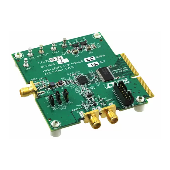
LTC2260-14/-12, LTC2259-14/-12, LTC2258-14/-12, LTC2257-14/-12,
LTC2256-14/-12, 14/12-Bit, 25Msps to 150Msps ADCs
Description
Demonstration circuit 1369A supports a family of
14/12-bit 25Msps to 150Msps ADCs. Each assembly
features one of the following devices: LTC2262-14 or
LTC2262-12, LTC2261-14, LTC2261-12, LTC2260-14,
LTC2260-12, LTC2259-14, LTC2259-12, LTC2258-14,
LTC2258-12, LTC2257-14, LTC2257-12, LTC2256-14,
LTC2256-12, high speed, high dynamic range ADCs.
Demonstration circuit 1369A supports the LTC2261 family
DDR LVDS output mode. This family of ADCs is also sup-
ported by demonstration circuit 1370A, which is compatible
with CMOS and DDR CMOS output modes.
performance summary
Table 1
PARAMETER
Supply Voltage – DC1369A
Analog Input Range
Logic Input Voltages
Logic Output Voltages (Differential)
Sampling Frequency (Convert Clock Frequency)
Convert Clock Level
Convert Clock Level
Resolution
Input Frequency Range
SFDR
SNR
DEMO MANUAL DC1369A
LTC2262-14/-12, LTC2261-14/-12,
Several versions of the 1369A demo board supporting the
LTC2261 14/12-bit series of A/D converters are listed in
Table 1. Depending on the required resolution and sample
rate, the DC1369A is supplied with the appropriate ADC.
The circuitry on the analog inputs is optimized for analog
input frequencies from 5MHz to 170MHz. Refer to the
data sheet for proper input networks for different input
frequencies.
Design files for this circuit board are available at
http://www.linear.com/demo
L, LT, LTC, LTM, Linear Technology and the Linear logo are registered trademarks and PScope
and QuikEval are trademarks of Linear Technology Corporation. All other trademarks are the
property of their respective owners.
(T
= 25°C)
A
CONDITION
Depending on sampling rate and the A/D converter
provided, this supply must provide up to 250mA
Depending on SENSE Pin Voltage
Minimum Logic High
Maximum Logic Low
Nominal Logic Levels (100Ω Load, 3.5mA Mode)
Minimum Logic Levels (100Ω Load, 3.5mA Mode)
See Table 1
Single-Ended Encode Mode (ENC – Tied to GND)
Differential Encode Mode (ENC – Not Tied to GND)
See Table 1
See Table 1
See Applicable Data Sheet
See Applicable Data Sheet
VALUE
Optimized for 3.6V
3.5V ↔ 6.0V Min/Max
1V
to 2V
P-P
P-P
1.3V
0.6V
350mV/1.25V Common Mode
247mV/1.25V Common Mode
0V to 3.6V
0.2V to 3.6V
dc1369af
1
Advertisement

Related Manuals for Linear Technology DC1369A


Summary of Contents for Linear Technology DC1369A
- Page 1 CMOS and DDR CMOS output modes. L, LT, LTC, LTM, Linear Technology and the Linear logo are registered trademarks and PScope and QuikEval are trademarks of Linear Technology Corporation. All other trademarks are the property of their respective owners.
-
Page 2: Quick Start Procedure
LTC2262 family of A/D converters. Demonstration Circuit Refer to Figure 1 for proper measurement equipment setup If a DC890 is used to acquire data from the DC1369A, and follow the procedure below: the DC890 must first be connected to a powered USB... - Page 3 DEMO MANUAL DC1369A Quick start proceDure 3.5V to 6V Jumpers Are Shown in Default Positions Analog Input Parallel Data Output to DC890 Parallel/Serial Programming Mode Duty Cycle Stabilizer DC1369A F01 SHDN Single-Ended Encode Clock Figure 1. DC1369A Setup dc1369af...
- Page 4 SNR. In the be driven with a very low jitter, square wave source. The case of the DC1369A a bandpass filter used for the clock or 13dBm. When amplitude should be large, up to 3V should be used prior to the DC1075A.
- Page 5 Collect button should result in time and frequency plots displayed in If the DC1369A demonstration circuit is properly connected the PScope window. Additional information and help for to the DC890, PScope should automatically detect the PScope is available in the DC890 Quick Start Guide and in DC1369A, and configure itself accordingly.
- Page 6 This menu allows any of the options available for the LTC2262 family to be programmed serially. The LTC2262 PScope has the ability to program the DC1369A board family has the following options: serially through the DC890. There are several options...
- Page 7 • Disabled: Disables digital outputs • Off (Default): Disables data output randomizer • On: Enables data output randomizer Output Mode: Selects Digital Output Mode • Full Rate: Full rate CMOS output mode (This mode is Two’s Complement: Enables Two’s Complement Mode not supported by the DC1369A, please use the DC1370) • Off (Default): Selects offset binary mode • Double LVDS (Default): Double data rate LVDS output • On: Selects two’s complement mode mode • Double CMOS: Double data rate CMOS output mode Once the desired settings are selected hit OK and PScope...
-
Page 8: Parts List
DEMO MANUAL DC1369A parts List ITEM REFERENCE PART DESCRIPTION MANUFACTURER/PART NUMBER RES, 0402 150Ω 1% 1/16W VISHAY CRCW0402150RFKED C2, C3, C6, C7, C38, C39, C59-C61 CAP , 0402 0.01uF 10% 16V X7R AVX 0402YC103KAT C10, C9 CAP , 0402 8.2pF 5% 50V COG... - Page 9 DEMO MANUAL DC1369A parts List ITEM REFERENCE PART DESCRIPTION MANUFACTURER/PART NUMBER XFMR, 1:4 CT COILCRAFT WBC4-1WLB IC, EEPROM MICROCHIP TECH. 24LC025-I/ST IC, FIN1108 FAIRCHILD FIN1108 IC, LDO Micropower Regulators LINEAR TECH. LT1763CDE-1.8 IC, 8-BIT I/0 EXPANDER PHILIPS SEMI PCF8574TS/3 IC, LDO Micropower Regulators LINEAR TECH.
- Page 10 DEMO MANUAL DC1369A schematic Diagram dc1369af...
-
Page 11: Schematic Diagram
Information furnished by Linear Technology Corporation is believed to be accurate and reliable. However, no responsibility is assumed for its use. Linear Technology Corporation makes no representa- tion that the interconnection of its circuits as described herein will not infringe on existing patent rights. - Page 12 Linear Technology Corporation (LTC) provides the enclosed product(s) under the following AS IS conditions: This demonstration board (DEMO BOARD) kit being sold or provided by Linear Technology is intended for use for ENGINEERING DEVELOPMENT OR EVALUATION PURPOSES ONLY and is not provided by LTC for commercial use. As such, the DEMO BOARD herein may not be complete in terms of required design-, marketing-, and/or manufacturing-related protective considerations, including but not limited to product safety measures typically found in finished commercial goods.
- Page 13 Mouser Electronics Authorized Distributor Click to View Pricing, Inventory, Delivery & Lifecycle Information: Analog Devices Inc. DC1369A-C DC1369A-D DC1369A-J DC1369A-N DC1369A-F DC1369A-G DC1369A-L DC1369A-K DC1369A-I DC1369A-M DC1369A-A DC1369A-H DC1369A-B DC1369A-E...
Need help?
Do you have a question about the DC1369A and is the answer not in the manual?
Questions and answers