Table of Contents
Advertisement
Quick Links
Advertisement
Table of Contents

Related Manuals for Renishaw RPI30


Summary of Contents for Renishaw RPI30
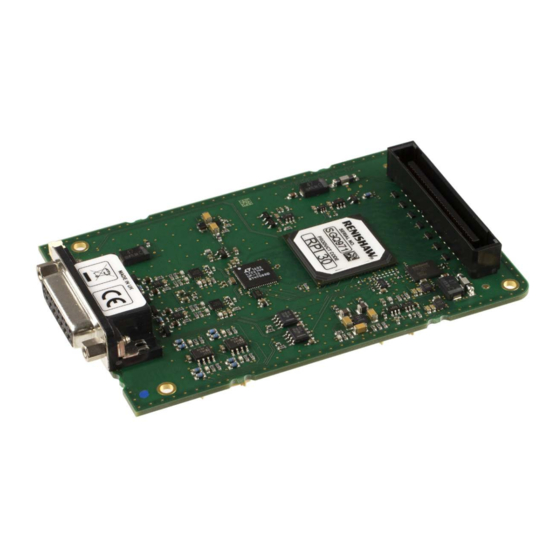
- Page 1 User’s guide F-9926-0018-01-B RPI30 parallel interface...
- Page 2 THE CONTENT OF THIS DOCUMENT IS CORRECT AT THE Changes to Renishaw products DATE OF PUBLICATION BUT MAKES NO WARRANTIES OR Renishaw plc reserves the right to improve, change or modify its REPRESENTATIONS REGARDING THE CONTENT. RENISHAW EXCLUDES LIABILITY, HOWSOEVER ARISING, FOR ANY products and documentation without incurring any obligation to make INACCURACIES IN THIS DOCUMENT.
- Page 3 Further information on safety is contained in Appendix B. The RPI30 has been designed for use with an RLE laser encoder only. Its use is not supported with other encoder systems.
- Page 4 Information required by Article 33(1) of Regulation (EC) No. 1907/2006 (“REACH”) relating to products containing substances of very high Renishaw plc declares that the RPI30 parallel interface complies with concern (SVHCs) is available at: the applicable directives, standards and regulations. A copy of the full www.renishaw.com/REACH...
-
Page 5: Table Of Contents
Lissajous correction status (Block = 8) ..29 RLE set-up – dip switches ....... 9 2.10 Lissajous correction control (Block = 9) ..30 RPI30 set-up ..........10 2.11 Data logger (Block = 10) ........ 31 /Error line ............11 Appendix D ................ -
Page 6: System Overview
Additionally the RPI30 has an separate diagnostics connection to allow diagnostics information to be downloaded and analysed remotely. The RPI30 gives an output of both axis position and status over a LVTTL (3.0 V) compatible bus. The position is available as a 36-bit two’s complement word, with a choice of least significant bit (LSB) resolution. -
Page 7: Installation
RPI30 assemblies to prevent damage from ESD. 2.2 Mounting and fixing The RPI30 can be supported using the four mounting holes (A, B, C and D) which are suitable for M3 screws. The position of the holes are shown within diagram opposite. All dimensions are in millimetres. -
Page 8: Analogue Quadrature Interface
WARNING: It is essential that the error line inputs are connected The RPI30 accepts the nominal 1 Vpp analogue quadrature from the so that the RPI30 can determine if any errors have occurred in RLE. Signal termination is contained within the RPI30 itself. There is no the RLE system. - Page 9 Connector pin out The analogue quadrature input connector pin out is shown in the table below. All pins are protected to ±7 V. The connector on the RPI30 is a 15 way female D-type. The diagram opposite shows the mating D-type connector.
-
Page 10: Analogue Feed Through
8-way picoblade connector. These are copies of the input signals diagnostic and control registers in addition to the normal SPI interface. and do not have any SDE correction appled or RPI30 errors included. Full details can be found in Appendix D. -
Page 11: Parallel Interface
Installation 2.6 Parallel interface Connector The correct mating connectors for the RPI30 parallel bus are the JAE TX24 60R family of connectors. These may be supplied by Renishaw or direct from JAE. Label Label Label Label DTA26 DTA19 DTA25 DTA18... - Page 12 Part number for JAE connector Note: using RPI mating 0º connector, A-9904-2256, separation between boards = 12 mm RPI30 parallel bus mating connector Other separations can be achieved using other receptacles. For detailed information on the connectors, please visit the JAE web site...
-
Page 13: Configuration
RLE DIP switches. The If the RPI30 is being used with an RLE system, care should be taken digital quadrature resolution and the digital output bandwidth should be setting the RLE configuration switches correctly. -
Page 14: Rpi30 Set-Up
Configuration 3.2 RPI30 set-up The SPI and UART interfaces also allow access to a variety of additional information including The settings for the parallel interface and lissajous correction are • RPI30 version accessible over the SPI interface and also the diagnostics UART interface. -
Page 15: Error Line
The parallel bus includes a /error line which is active low. The /error line WARNING: The open collector /error line is not a fail-safe method indicates if any errors have occurred with either the RLE or the RPI30. and therefore additional safety precautions must be taken in The /error line is latched if an error occurs and must be cleared by a safety critical closed loop applications. -
Page 16: Communication Over The Parallel Bus
4 Communication over the parallel Data bus The RPI30 can be requested to put either position or status data on the data bus. The position data is a 36-bit word with DTA0 as the LSB and High speed communication with the RPI30 is performed over the DTA35 as the MSB. -
Page 17: Functionality
Function Five functions may be performed over the parallel bus. These are: Latch all RPI30 units 1. Resetting the position and error status of the RPI30 Reserved Reset all RPI30 units 2. Latching the position and status reading of all... - Page 18 Reset Enable position data Register 3 is used to reset the RPI30. If there are no errors currently Register 1 of a particular RPI30 unit’s base address holds the latched active in the system, the /error line is reset, any latched error flags position data.
- Page 19 Enable status data Enable test data Register 2 of a particular RPI30 unit holds the latched status information. If Register 4 of a particular RPI30 unit holds test information which this register is selected on the address bus, the status information is placed can be used for checking the data bus for open and short circuits on the data bus after the /enable line is taken low.
-
Page 20: Timing Diagram
3. Read in position data from axis 2 by taking /enable low whilst the address bus is set to 01000b (base address 2, register 1) ** The same timing sequence should be used to reset an RPI30. Sample Sin Cos... - Page 21 /Enable to data valid Data valid to hi-impedance state Propagation delay. The time before the /Enable that the position event occurred. This defines the delay due to RPI30 only. Time between sequential axis access Minimum period that /Enable must be high...
-
Page 22: Appendix A - Specification
Specification Appendix A – Specification Values in this table define the contribution of the RPI30 on the system performance, NOT the Voltage 5 V ±0.25 V complete laser interferometer system performance. Operating current 500 mA Noise and ripple 50 mVpp (DC to 10 MHz) RPI30 power requirement 38.6, 77.2,... -
Page 23: Appendix B - Safety Information
It is important to set the LSB resolution of the RPI30 correctly. If the 1. The RPI30 includes an error signal output. The control system must LSB resolution is set incorrectly, the axis may move for distances and at be designed to stop the axis motion if this error is asserted. - Page 24 RPI30 unit. Position data integrity If an error is signalled by the RPI30, then the RPI30 position data may be incorrect. The system must be reset and re-referenced before it is...
-
Page 25: Spi Programming Guide
SPI programming guide Appendix C 1.2 Command makeup The command byte defines whether the operation is a read or write SPI programming guide and the register it is addressing. The data in the response to a write command is the previous contents of the addressed register. The 1.1 Timing address is made up of two parts, 4 bits for the block of registers and 3 bits for the register. -
Page 26: Registers
Hard reset FPGA Offset Cosine EEPROM Read User calibration Scale Sine Write settings to EEPROM Scale Cosine Enable write EEPROM ADC source Reserved Renishaw use ADC 1 Lissajous Offset Sin ADC 2 latched correction Offset Cos ADC 2 unlatched status... -
Page 27: Version (Block = 0)
SPI programming guide 2.2.2 PCB revision (Sub = 1) Lissajous Enable correction Read only register containing the PCB revision in the least significant Sampling length control four bits. All other bits read as 0. Min Quads 2.2.3 Serial number (Sub = 2 – 5) Max Quads Offset filter length Read only registers containing the serial number in the form of 10 ASCII... - Page 28 SPI programming guide 2.3.2 Gain Sine/Cosine (Sub = 2, 3) Zeros Zeros Read / write register containing an 18-bit signed integer scale factor Zeros Zeros where 32768 is defined as a gain of 1. The scale factor is set such that After offset/gain correction a 1Vp-p input gives 100% signal strength.
-
Page 29: Interpolator (Block = 2)
Read only registers containing the full internal 44-bit position sign convert to signal strength (100% = 1V p-p) divide by 20.47. extended to 48-bits in two registers, it isn’t affected by the RPI30 emulation resolution setting. The high bytes register (1) is latched on... - Page 30 SPI programming guide changes, an error is raised which is reported in the error register and 23 - 2 1 - 0 on the parallel bus status as bus settings changed. Valid address range Definition Don’t care Resolution (approx. LSB is 1-7, address 0 can be written but the bus will not be driven when for plane mirror) address 0 is selected.
-
Page 31: Reset / Errors (Block = 5)
2.7.2 Reset errors (Sub = 1) command from one of the RPI30, diagnostics or SPI interfaces. Writing anything to this register resets the current errors and warnings if the condition is no longer present. The errors and warnings can also be reset via the parallel bus. -
Page 32: Eeprom (Block = 6)
Reset angle offset (Sub = 4) Write settings to EEPROM register definition Writing anything to this register resets the angle offset to 0. The RPI30 and lissajous correction settings are read on power up to 2.7.6 Reset ADC min/max (Sub = 5) initialise the board (and when the reset FPGA command is sent). -
Page 33: Lissajous Correction Status (Block = 8)
SPI programming guide 2.9 Lissajous correction status (Block = 8) 2.9.6 Status (Sub = 6) 2.9.1 Offset (Sub = 0, 1) Read only register containing the status of the auto correction for the last sample period. Read only registers containing the offsets applied to Sine and Cosine signals in the auto correction. -
Page 34: Lissajous Correction Control (Block = 9)
SPI programming guide 2.10 Lissajous correction control (Block = 9) Setting the bypass bit takes the phase correction out of the signal path, the output of the offset and AC mismatch correction is fed directly into 2.10.1 Enable (Sub = 0) the interpolator. -
Page 35: Data Logger (Block = 10)
SPI programming guide 2.10.5 Offset and AC filter length (Sub = 4, 5) 2.10.6 Phase filter length (Sub = 6) Read / write register containing the settings for the offset and AC Future functionality. mismatch filters. 2.11 Data logger (Block = 10) 23 - 3 1 - 0 Definition Don’t care The data logger collects 28672 samples of 6 bytes. The samples can Filter length be either ADC data selected from any of the monitor options, or position 00 –... - Page 36 SPI programming guide 2.11.4 Control (Sub = 4) ADC data and source are the same format as for direct reading of the ADC. The definition of the bits in the error byte are given in Table 3-27. To start data logging write 1 to bit 0, bit 1 is then set when the logging finishes.
-
Page 37: Diagnostics Link
UART running at 3M baud, 1 start bit, 8 data bits and 1 stop bit. Check sum Negative of the sum of the previous bytes Connection is via a 6-way PicoBlade connector on the side of the RPI30. Register access packet format. If the received packet has an incorrect checksum then no response is sent. -
Page 38: Diagnostics (Block = 15)
Diagnostics 2.2 Diagnostics (Block = 15) 23 - 10 19 - 8 7 - 3 2 - 1 Function Zeros Start address Zeros Number of Start 2.2.1 Streaming enable (Sub = 0) packets download 0 - 3583 Reading registers individually is a relatively slow process, in order to 00 –... -
Page 39: Streaming Data
Diagnostics Streaming data AC byte 0 24-bit signed Correction – integer AC mismatch scale factor AC byte 1 3.1 Packet format AC byte 2 Phase 1 byte 0 24-bit signed Correction – phase scale factor The streaming data packet is 34 bytes long and transmitted at the rate integer Phase 1 byte 1 defined in the streaming enable register. -
Page 40: Download Datalogger Ram
Diagnostics Download datalogger RAM The RAM download packet is 52 bytes long, consisting of 8 48-bit samples and the start address. The data is transmitted least significant byte first. Data format is the same as the equivalent data logger data registers. - Page 41 Renishaw plc +44 (0)1453 524524 +44 (0)1453 524901 New Mills, Wotton-under-Edge, uk@renishaw.com Gloucestershire, GL12 8JR United Kingdom www.renishaw.com For worldwide contact details, please visit our main web site at www.renishaw.com/contact *F-9926-0018-01*...
Need help?
Do you have a question about the RPI30 and is the answer not in the manual?
Questions and answers