Table of Contents
Advertisement
Quick Links
We have 45,000 LP502030-PCM-NTC-LD-A02554 - EEMB - Lithium Battery Rectangular 3.7V 250mAh Rechargeable in
stock now. Starting at $0.034. This EEMB part is fully warrantied and traceable.
Looking for a discount?
Check out our current promotions!
This coversheet was created by Verical, a division of Arrow Electronics, Inc. ("Verical"). The attached document was created by the part supplier,
not Verical, and is provided strictly 'as is.' Verical, its subsidiaries, affiliates, employees, and agents make no representations or warranties
regarding the attached document and disclaim any liability for the consequences of relying on the information therein. All referenced brands,
product names, service names, and trademarks are the property of their respective owners.
00000005981LF-000
LS1043ARDB-PA
EOS Power
FREESCALE
Buy Now
Buy Now
Give us a call
1-855-837-4225
International: 1-555-555-5555
1-415-281-3866
1-415-281-3866
Arrow Electronics,
Arrow Electronics, Inc
Verical Division
9201 East Dry Creek Road
P.O. Box 740970
Centennial, CO 80112
Los Angeles, CA 90074-0970
Advertisement
Table of Contents

Subscribe to Our Youtube Channel
Related Manuals for Freescale Semiconductor QorIQ LS1043A


Summary of Contents for Freescale Semiconductor QorIQ LS1043A
- Page 1 We have 45,000 LP502030-PCM-NTC-LD-A02554 - EEMB - Lithium Battery Rectangular 3.7V 250mAh Rechargeable in stock now. Starting at $0.034. This EEMB part is fully warrantied and traceable. 00000005981LF-000 LS1043ARDB-PA EOS Power FREESCALE Buy Now Buy Now Looking for a discount? Check out our current promotions! Give us a call 1-855-837-4225...
- Page 2 QorIQ LS1043A Reference Design Board Reference Manual Document Number: LS1043ARDBRM Rev. 0, 08/2015...
- Page 3 QorIQ LS1043A Reference Design Board Reference Manual, Rev. 0, 08/2015 Freescale Semiconductor, Inc.
-
Page 4: Table Of Contents
Mini-PCIe card..............................27 2.6 USB interface..................................28 2.7 I2C interface..................................29 Chapter 3 Power Supplies and CPLD Controller 3.1 Power supply block diagram.............................33 3.2 Power supply operation..............................34 3.2.1 Power ON................................34 QorIQ LS1043A Reference Design Board Reference Manual, Rev. 0, 08/2015 Freescale Semiconductor, Inc. - Page 5 PCBA version register (CPLD_PCBA_VER)..................... 53 6.1.4 System reset register (CPLD_SYSTEM_RST)....................53 6.1.5 CPLD override physical switches enable register (CPLD_SOFT_MUX_ON)...........54 6.1.6 POR RCW source location register 1 (CPLD_REG_RCW_SRC1)..............55 QorIQ LS1043A Reference Design Board Reference Manual, Rev. 0, 08/2015 Freescale Semiconductor, Inc.
- Page 6 6.1.13 SDHC or SPI_CS selection register (CPLD_SDHC_SPICS_SEL)..............59 6.1.14 Status LED control register (CPLD_STATUS_LED)..................60 6.1.15 Global reset register (CPLD_GLOBAL_RST)....................60 6.1.16 TDM riser card presence detection register (CPLD_TDMR_PRS_N)..............61 6.1.17 RTC clock assignment register (CPLD_REG_RTC)...................61 QorIQ LS1043A Reference Design Board Reference Manual, Rev. 0, 08/2015 Freescale Semiconductor, Inc.
- Page 7 QorIQ LS1043A Reference Design Board Reference Manual, Rev. 0, 08/2015 Freescale Semiconductor, Inc.
- Page 8 Introduction The LS1043A reference design board (RDB) is a high-performance computing, evaluation, and development platform that supports the QorIQ LS1043A LayerScape architecture processor. The LS1043ARDB provides software development platform for the Freescale LS1043A processor series, with a complete debugging environment. It functions as a desktop computer and operates as a development and evaluation system.
-
Page 9: Acronyms And Abbreviations
Inter-integrated circuit multi-master serial computer bus Integrated flash controller Initial program load JTAG Joint Test Action Group (IEEE® standard 1149.1™) LBMAP Local bus map Table continues on the next page... QorIQ LS1043A Reference Design Board Reference Manual, Rev. 0, 08/2015 Freescale Semiconductor, Inc. - Page 10 Serial gigabit media-independent interface SLAC Subscriber line access controller Single-level cell SLIC Subscriber line interface controller Subminiature version B connector Serial presence detect Table continues on the next page... QorIQ LS1043A Reference Design Board Reference Manual, Rev. 0, 08/2015 Freescale Semiconductor, Inc.
-
Page 11: Related Documentation
Provides details of all known silicon errata for the LS1043A processor NOTE Some of the documents listed in the table above, may be available only under a non-disclosure agreement (NDA). To QorIQ LS1043A Reference Design Board Reference Manual, Rev. 0, 08/2015 Freescale Semiconductor, Inc. -
Page 12: Board Features
100 MHz • Supports single-source differential DIFF_SYCLK_/DIFF_SYSCLK_N, 100 MHz SerDes • Provides clocks to all SerDes blocks and slots Table continues on the next page... QorIQ LS1043A Reference Design Board Reference Manual, Rev. 0, 08/2015 Freescale Semiconductor, Inc. -
Page 13: Block Diagrams
• 3.3 V / 1.8 V for eSDHC • 1.0 V for security monitor (VDD_LP) 1.4 Block diagrams The figure below shows the LS1043A processor block diagram. QorIQ LS1043A Reference Design Board Reference Manual, Rev. 0, 08/2015 Freescale Semiconductor, Inc. - Page 14 Chapter 1 Introduction Figure 1-1. LS1043A processor block diagram The figure below shows the LS1043ARDB block diagram. QorIQ LS1043A Reference Design Board Reference Manual, Rev. 0, 08/2015 Freescale Semiconductor, Inc.
-
Page 15: Board Drawings
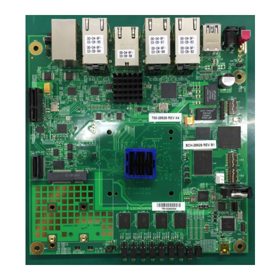
Board drawings Figure 1-2. LS1043ARDB block diagram 1.5 Board drawings The figure below shows the LS1043ARDB top view. QorIQ LS1043A Reference Design Board Reference Manual, Rev. 0, 08/2015 Freescale Semiconductor, Inc. - Page 16 Chapter 1 Introduction Figure 1-3. LS1043ARDB top view The figure below shows the LS1043ARDB bottom view. QorIQ LS1043A Reference Design Board Reference Manual, Rev. 0, 08/2015 Freescale Semiconductor, Inc.
- Page 17 Board drawings Figure 1-4. LS1043ARDB bottom view QorIQ LS1043A Reference Design Board Reference Manual, Rev. 0, 08/2015 Freescale Semiconductor, Inc.
-
Page 18: Interfaces
SDRAM discrete devices (32-bit bus). The memory interface includes all necessary termination and I/O powers. It is routed such that maximum performance of the memory bus can be achieved. The figure below shows the DDR memory architecture. QorIQ LS1043A Reference Design Board Reference Manual, Rev. 0, 08/2015 Freescale Semiconductor, Inc. -
Page 19: Ifc Interface
• Supports the following IFC clients on the LS1043ARDB: • NAND flash (async/sync - ONFI 1.0 compatible) • NOR flash 16-bit The figure below shows the IFC block diagram. QorIQ LS1043A Reference Design Board Reference Manual, Rev. 0, 08/2015 Freescale Semiconductor, Inc. -
Page 20: Nor Flash Memory
Data width 000100101 NOR flash 16 bits NAND flash 8 bits CPLD registers 8 bits 100000101 NAND flash 8 bits NOR flash 16 bits CPLD registers 8 bits QorIQ LS1043A Reference Design Board Reference Manual, Rev. 0, 08/2015 Freescale Semiconductor, Inc. -
Page 21: Nand Flash Memory
The LS1043ARDB has several serial interfaces, such as RS-232, DSPI, eSDHC/eMMC, and I2C. This section describes the following main serial interfaces used in the LS1043ARDB: • UART interface • eSDHC interface • DSPI interface QorIQ LS1043A Reference Design Board Reference Manual, Rev. 0, 08/2015 Freescale Semiconductor, Inc. -
Page 22: Uart Interface
UART2 (J4 top) 2.3.2 eSDHC interface The LS1043ARDB enhanced secure digital high capacity card (eSDHC) has the following features: • x1/x4-bit SD card supporting SD Rev 2.0 and 3.0. QorIQ LS1043A Reference Design Board Reference Manual, Rev. 0, 08/2015 Freescale Semiconductor, Inc. - Page 23 Supply voltage negative Pin 5 Supply voltage positive Pin 6 Clock signal Pin 7 Supply voltage negative Pin 8 DAT0 Data signal 0 Pin 9 DAT1 Data signal 1 QorIQ LS1043A Reference Design Board Reference Manual, Rev. 0, 08/2015 Freescale Semiconductor, Inc.
-
Page 24: Dspi Interface
Figure 2-5. DSPI connections NOTE Some DSPI pins are muxed with eSDHC pins; therefore, DSPI functionality depends on the eSDHC configuration. The table below describes the LS1043ARDB SPI flash memory. QorIQ LS1043A Reference Design Board Reference Manual, Rev. 0, 08/2015 Freescale Semiconductor, Inc. -
Page 25: Ethernet Interface
Address 2 RTL8211FS eTSEC1 Address 1 MDIO/MDC EMI1_MDC/MDIO Figure 2-6. Ethernet interface Connections and routing for the three-speed Ethernet controller (TSEC) are summarized in the table below. QorIQ LS1043A Reference Design Board Reference Manual, Rev. 0, 08/2015 Freescale Semiconductor, Inc. -
Page 26: Mii Buses
EMI2) that are used to control two separate PHY transceiver devices. The MII buses are connected to the Realtek, QSGMII, and Aquantia AQR105-B1 PHYs. The figure below shows how the PHY devices are connected to the MII management buses. QorIQ LS1043A Reference Design Board Reference Manual, Rev. 0, 08/2015 Freescale Semiconductor, Inc. -
Page 27: Serdes Interface
2.5 SerDes interface The serializer/deserializer (SerDes) block of the LS1043ARDB supports several protocols that includes four serial lanes. See QorIQ LS1043A Reference Manual (LS1043ARM) for information on supported SerDes combinations. The table below lists the SerDes embedded devices used on the LS1043ARDB. -
Page 28: Mini-Pcie Card
QSGMII Rx/Tx 1 (4x1.25G) eth0 Mini-PCIe slot eth4 Rx/Tx 2 (PCIe 2) PCIe slot x1 Rx/Tx 3 (PCIe 3) Figure 2-8. LS1043ARDB SerDes lane connections QorIQ LS1043A Reference Design Board Reference Manual, Rev. 0, 08/2015 Freescale Semiconductor, Inc. -
Page 29: Usb Interface
5 V power at up to 1.2 A. The power enable and power-fault-detect pins are connected to the LS1043A processor via CPLD for individual port management. The figure below shows the LS1043ARDB USB architecture. QorIQ LS1043A Reference Design Board Reference Manual, Rev. 0, 08/2015 Freescale Semiconductor, Inc. -
Page 30: I2C Interface
• LS1043A I2C2, I2C3, and I2C4 are not used as I2C but they are used as other multiplexed pin functions. The figure below shows the overall I2C scheme connections. QorIQ LS1043A Reference Design Board Reference Manual, Rev. 0, 08/2015 Freescale Semiconductor, Inc. - Page 31 Real-time clock (RTC) Semiconductor I2C address is Mini-PCIe slot defined by the plugged-in PEX card I2C address is X1 PEX slot defined by the plugged-in PEX card QorIQ LS1043A Reference Design Board Reference Manual, Rev. 0, 08/2015 Freescale Semiconductor, Inc.
- Page 32 7-bit addresses do not include the R/W bit as an address member, though some datasheets might do so. For consistency, all I2C addresses are of 7 bits only. QorIQ LS1043A Reference Design Board Reference Manual, Rev. 0, 08/2015 Freescale Semiconductor, Inc.
- Page 33 I2C interface QorIQ LS1043A Reference Design Board Reference Manual, Rev. 0, 08/2015 Freescale Semiconductor, Inc.
-
Page 34: Power Supplies And Cpld Controller
3.1 Power supply block diagram The figure below shows the LS1043ARDB power supply block diagram. QorIQ LS1043A Reference Design Board Reference Manual, Rev. 0, 08/2015 Freescale Semiconductor, Inc. -
Page 35: Power Supply Operation
• Power ON • Power sequencing 3.2.1 Power ON The SW2 switch, which is on the rear panel enables the 12 V power supply for the board. QorIQ LS1043A Reference Design Board Reference Manual, Rev. 0, 08/2015 Freescale Semiconductor, Inc. -
Page 36: Cpld Controller
• Control status LED • Map/re-map the LS1043A local bus chip selects and ready and busy signals to NOR flash and NAND flash • IFC bus control: QorIQ LS1043A Reference Design Board Reference Manual, Rev. 0, 08/2015 Freescale Semiconductor, Inc. -
Page 37: Cpld Block Diagram
• NOR bank selection: Split NOR flash into 8 banks. 3.3.2 CPLD block diagram The figure below shows a detailed block diagram of the CPLD controller on the LS1043ARDB. QorIQ LS1043A Reference Design Board Reference Manual, Rev. 0, 08/2015 Freescale Semiconductor, Inc. -
Page 38: Cpld Registers
LS1043ARDB. These registers can be accessed from CPLD using IFC. The table below shows the peripheral data bus width and memory map for CPLD. QorIQ LS1043A Reference Design Board Reference Manual, Rev. 0, 08/2015 Freescale Semiconductor, Inc. -
Page 39: Power-On Reset
HRESET_B indicates the hard reset input signal. It is a bi-directional open drain signal. It functions as an output signal during initial steps in the POR sequence. The table below describes the POR sequence. QorIQ LS1043A Reference Design Board Reference Manual, Rev. 0, 08/2015 Freescale Semiconductor, Inc. -
Page 40: Reset Configuration Signals
CFG_RCW_SRC3 IFC_AD10 SW4[4] Specifies RCW fetch location CFG_RCW_SRC4 IFC_AD11 SW4[5] Specifies RCW fetch location CFG_RCW_SRC5 IFC_AD12 SW4[6] Specifies RCW fetch location Table continues on the next page... QorIQ LS1043A Reference Design Board Reference Manual, Rev. 0, 08/2015 Freescale Semiconductor, Inc. -
Page 41: Reset Architecture
The reset signals sent to and received from the LS1043A processor and other devices on the LS1043ARDB are managed by the CPLD controller. The figure below shows the LS1043ARDB reset architecture. QorIQ LS1043A Reference Design Board Reference Manual, Rev. 0, 08/2015 Freescale Semiconductor, Inc. -
Page 42: Ddr Supply
<= 1 A Bus termination supply +2V5_VPP 2.5 V < 200 mA DRAM activating power supply The LS1043ARDB uses the VR500 (U33) switching power controller as follows: QorIQ LS1043A Reference Design Board Reference Manual, Rev. 0, 08/2015 Freescale Semiconductor, Inc. -
Page 43: Povdd Supply
3.6 POVDD supply J12 and J13 connectors on the LS1043ARDB connect POVDD power line to LS1043A PROG_MTR and PROG_SFP pins. Otherwise, they are pulled down to the ground plane. QorIQ LS1043A Reference Design Board Reference Manual, Rev. 0, 08/2015 Freescale Semiconductor, Inc. -
Page 44: Clocks, Interrupts, And Temperature Monitoring
Temperature anode and cathode 4.1 Clocking scheme The figure below shows the LS1043ARDB clocking scheme. NOTE For RDBs, Freescale does not support spread spectrum for SerDes clocking. QorIQ LS1043A Reference Design Board Reference Manual, Rev. 0, 08/2015 Freescale Semiconductor, Inc. -
Page 45: Clock Frequency Selection
The table below shows how to select SYSCLK frequency based on the settings of the SW3 switch. Table 4-1. SYSCLK frequency selection SW3[1] SW3[2] Selected SYSCLK frequency 66.67 MHz 100.00 MHz (default value) 80.00 MHz Table continues on the next page... QorIQ LS1043A Reference Design Board Reference Manual, Rev. 0, 08/2015 Freescale Semiconductor, Inc. -
Page 46: Mpic Controller
ADT7461 temperature warning and alarm signals are used to drive indicators and are connected to CPLD for monitoring. CPLD uses these signals to power down the system to protect the LS1043ARDB from over-temperature failure. QorIQ LS1043A Reference Design Board Reference Manual, Rev. 0, 08/2015 Freescale Semiconductor, Inc. - Page 47 Temperature anode and cathode QorIQ LS1043A Reference Design Board Reference Manual, Rev. 0, 08/2015 Freescale Semiconductor, Inc.
-
Page 48: Debug And Input/Output
Debug and Input/Output This chapter contains the following sections: • ARM/JTAG architecture • CMSIS-DAP • GPIOs 5.1 ARM/JTAG architecture The ARM/JTAG architecture is shown in the figure below. QorIQ LS1043A Reference Design Board Reference Manual, Rev. 0, 08/2015 Freescale Semiconductor, Inc. -
Page 49: Cmsis-Dap
This section describes the MBED circuit on the LS1043ARDB. MBED is an open standard serial and debug adapter. It bridges serial and debug communications between a USB host and an embedded target processor, as shown in the figure below. QorIQ LS1043A Reference Design Board Reference Manual, Rev. 0, 08/2015 Freescale Semiconductor, Inc. -
Page 50: Gpios
GPIO_4[6] to GPIO_4[9] can be used to drive four LED signals. The names of the GPIO pins with and without test point access are shown in the table below. QorIQ LS1043A Reference Design Board Reference Manual, Rev. 0, 08/2015 Freescale Semiconductor, Inc. - Page 51 IRQ[8] GPIO1_28 TDMB_RXD TDM slot IRQ[9] GPIO1_29 TDMB_RSYNC TDM slot IRQ[10] GPIO1_30 TDMB_TXD TDM slot IRQ[11] GPIO1_31 CPLD ASLEEP GPIO1_13 ALEEP LED GPIO1_14 RTC CLK RTC clock QorIQ LS1043A Reference Design Board Reference Manual, Rev. 0, 08/2015 Freescale Semiconductor, Inc.
-
Page 52: Cpld Programming
TDM clock or SDHC/USB selection register See section 6.1.12/59 (CPLD_TDMCLK_MUX_SEL) SDHC or SPI_CS selection register See section 6.1.13/59 (CPLD_SDHC_SPICS_SEL) Status LED control register (CPLD_STATUS_LED) 6.1.14/60 Table continues on the next page... QorIQ LS1043A Reference Design Board Reference Manual, Rev. 0, 08/2015 Freescale Semiconductor, Inc. -
Page 53: Cpld Major Version Register (Cpld_Ver)
6.1.2 CPLD minor version register (CPLD_VER_SUB) Use this register to specify CPLD minor version. Address: 0h base + 1h offset = 1h Read VER_SUB Reserved Write Reset QorIQ LS1043A Reference Design Board Reference Manual, Rev. 0, 08/2015 Freescale Semiconductor, Inc. -
Page 54: Pcba Version Register (Cpld_Pcba_Ver)
Address: 0h base + 3h offset = 3h Read SYSTEM_ Reserved Write Reset CPLD_SYSTEM_RST field descriptions Field Description System reset SYSTEM_RST Table continues on the next page... QorIQ LS1043A Reference Design Board Reference Manual, Rev. 0, 08/2015 Freescale Semiconductor, Inc. -
Page 55: Cpld Override Physical Switches Enable Register (Cpld_Soft_Mux_On)
SerDes PLL1 reference clock input control enable SD1REFCLK_ SerDes PLL1 reference clock input control disable (default value) IN_CTRL_EN SerDes PLL1 reference clock input control enable Table continues on the next page... QorIQ LS1043A Reference Design Board Reference Manual, Rev. 0, 08/2015 Freescale Semiconductor, Inc. -
Page 56: Por Rcw Source Location Register 1 (Cpld_Reg_Rcw_Src1)
Use this register to configure RCW source bits 0-7. Address: 0h base + 5h offset = 5h Read CFG_RCW_SRC[7:0] Write Reset CPLD_REG_RCW_SRC1 field descriptions Field Description 0–7 POR RCW source location CFG_RCW_ SRC[7:0] QorIQ LS1043A Reference Design Board Reference Manual, Rev. 0, 08/2015 Freescale Semiconductor, Inc. -
Page 57: Por Rcw Source Location Register 2 (Cpld_Reg_Rcw_Src2)
Address: 0h base + 7h offset = 7h Read BANK_CTRL Reserved Write Reset CPLD_REG_BANK field descriptions Field Description 0–2 Bank control bits BANK_CTRL 3–7 This field is reserved. QorIQ LS1043A Reference Design Board Reference Manual, Rev. 0, 08/2015 Freescale Semiconductor, Inc. -
Page 58: System Clock Single-Ended Or Differential Input Selection Register (Cpld_Sysclk_Sel)
Address: 0h base + 9h offset = 9h Read UART1_ Reserved Write OUT_SEL Reset CPLD_UART_SEL field descriptions Field Description UART1 output selection UART1_OUT_ Table continues on the next page... QorIQ LS1043A Reference Design Board Reference Manual, Rev. 0, 08/2015 Freescale Semiconductor, Inc. -
Page 59: Serdes Pll1 Reference Clock Input Selection Register (Cpld_Sd1Refclk_Sel)
Read Reserved Write Reset CPLD_SD1REFCLK_SEL field descriptions Field Description SerDes PLL1 reference clock input selection SD1REFCLK_ 100 MHz (default value) 156.25 MHz 1–7 This field is reserved. QorIQ LS1043A Reference Design Board Reference Manual, Rev. 0, 08/2015 Freescale Semiconductor, Inc. -
Page 60: Tdm Clock Or Sdhc/Usb Selection Register (Cpld_Tdmclk_Mux_Sel)
Address: 0h base + Ch offset = Ch Read SDHC_ Reserved Write SPICS_SEL Reset CPLD_SDHC_SPICS_SEL field descriptions Field Description SDHC or SPI_CS selection SDHC_SPICS_ SDHC SPI_CS 1–7 This field is reserved. QorIQ LS1043A Reference Design Board Reference Manual, Rev. 0, 08/2015 Freescale Semiconductor, Inc. -
Page 61: Status Led Control Register (Cpld_Status_Led)
Address: 0h base + Eh offset = Eh Read GLOBAL_ Reserved Write Reset CPLD_GLOBAL_RST field descriptions Field Description System is running (default value) GLOBAL_RST System is reset 1–7 This field is reserved. QorIQ LS1043A Reference Design Board Reference Manual, Rev. 0, 08/2015 Freescale Semiconductor, Inc. -
Page 62: Tdm Riser Card Presence Detection Register (Cpld_Tdmr_Prs_N)
RTC clock assignment to RTC or TA_BB_RTC (only assert from LS1043ARDB Rev. B board) RTC_CLK_ To TA_BB_RTC (default value) ASSGNMT To RTC Table continues on the next page... QorIQ LS1043A Reference Design Board Reference Manual, Rev. 0, 08/2015 Freescale Semiconductor, Inc. - Page 63 CPLD memory map / register definitions CPLD_REG_RTC field descriptions (continued) Field Description 1–7 This field is reserved. QorIQ LS1043A Reference Design Board Reference Manual, Rev. 0, 08/2015 Freescale Semiconductor, Inc.
- Page 64 Appendix A Revision History The table below provides the revision history of this document. Revision Date Topic cross-reference Change description number Rev. 0 08/2015 Initial public release QorIQ LS1043A Reference Design Board Reference Manual, Rev. 0, 08/2015 Freescale Semiconductor, Inc.
- Page 65 QorIQ LS1043A Reference Design Board Reference Manual, Rev. 0, 08/2015 Freescale Semiconductor, Inc.
- Page 66 Freescale, the Freescale logo, and QorIQ are trademarks of Freescale Semiconductor, Inc., Reg. U.S. Pat. & Tm. Off. Layerscape and QUICC Engine are trademarks of Freescale Semiconductor, Inc. All other product or service names are the property of their respective owners.
Need help?
Do you have a question about the QorIQ LS1043A and is the answer not in the manual?
Questions and answers