Table of Contents
Advertisement
2020/02/27 22:53:44 (GMT+09:00)
SERVICE MANUAL
Ver. 1.3 2020.02
Note:
Be sure to keep your PC used for service and
checking of this unit always updated with the
latest version of your anti-virus software.
In case a virus aff ected unit was found during
service, contact your Service Headquarters.
• HCD-SX7 is the compact disc receiver in CMT-SX7.
• HCD-SX7B is the compact disc receiver in CMT-SX7B.
Amplifier section
Power output (rated):
30 watts + 30 watts (at 6 ohms, 1 kHz, 1%
THD) (Except Canadian model)
40 watts + 40 watts (at 6 ohms, 1 kHz, 1%
THD) (Canadian model)
RMS power output (reference):
50 watts + 50 watts (per channel at 6 ohms,
1 kHz)
Inputs/Outputs
LINE IN (external input) jack:
Sensitivity: 2 V
Impedance: 47 kilo ohms
OPTICAL IN (optical digital input) jack
(headphone) jack:
Stereo mini jack, 8 ohms or more
Section for USB port
(USB FRONT) port
You can connect a USB flash drive,
Walkman®, or iPhone/iPad/iPod that is
compatible with this system.
Supported format*
MP3: 32/44.1/48 kHz, 16 - 320 kbps (CBR/
VBR)
2
AAC*
: 32/44.1/48/88.2/96 kHz, 16 - 320
kbps (CBR/VBR)
2
WMA*
: 32/44.1/48 kHz, 16 - 320 kbps (CBR/
VBR)
WAV: 32/44.1/48/88.2/96/176.4/192 kHz
(16/24 bit)
AIFF: 32/44.1/48/88.2/96/176.4/192 kHz (16/
24 bit)
FLAC: 32/44.1/48/88.2/96/176.4/192 kHz
(16/24 bit)
ALAC: 32/44.1/48/88.2/96/176.4/192 kHz
(16/24 bit)
3
DSD*
(DSF/DSDIFF): 2.8 MHz (1bit)
Transfer speed
High-speed
Supported USB device
Mass Storage Class (MSC)
Maximum output current
2.1 A MAX
(USB REAR) port
You can connect a compatible device such
as a PC, etc., to this unit using a USB cable
(not supplied).
Supported format*
PCM: 44.1/48/88.2/96/176.4/192 kHz (16/
24/32 bit)
DSD (DSF/DSDIFF): 2.8 MHz (1 bit)
1
*
Compatibility with all encoding/writing
software, recording devices and recording
media cannot be guaranteed.
2
*
Files with DRM (Digital Rights Management)
copyright protection or files downloaded from
an online music store cannot be played on this
system. If you try to play one of these files, the
system plays the next unprotected audio file.
*
3
Output by converting to PCM.
9-896-163-04
2020B33-1
©
2020.02
HCD-SX7/SX7B
CD-DA/MP3 player section
System:
Compact disc and digital audio system
Laser Diode Properties:
Emission Duration: Continuous
1
Laser Output*
: Less than 44.6 μW
1
*
This output is the value measurement at a
distance of 200mm from the objective lens
surface on the Optical Pick-up Block with 7mm
aperture.
Frequency response:
20 Hz – 20 kHz
Signal-to-noise ratio:
More than 90 dB
Dynamic range:
More than 90 dB
Tuner section
AM tuner section (HCD-SX7 only):
Tuning range:
European models:
531 kHz – 1,602 kHz (with 9 kHz tuning
interval)
1
Asian models:
530 kHz – 1,610 kHz (with 10 kHz tuning
interval)
531 kHz – 1,602 kHz (with 9 kHz tuning
interval)
Other models:
530 kHz – 1,710 kHz (with 10 kHz tuning
interval)
531 kHz – 1,710 kHz (with 9 kHz tuning
interval)
Intermediate frequency:
400 kHz
FM tuner section:
FM stereo, FM superheterodyne tuner
Tuning range:
87.5 MHz – 108.0 MHz (50 kHz step)
(Except Canadian model)
87.5 MHz – 108.0 MHz (100 kHz step)
(Canadian model)
DAB/DAB+ tuner section (HCD-SX7B only):
FM stereo, DAB/FM superheterodyne tuner
Frequency range:
Band-III:
174.928 (5A) MHz – 239.200 (13F) MHz*
DAB/DAB+ frequency table (Band-III):
1
Frequency
Label
174.928 MHz
5A
176.640 MHz
5B
178.352 MHz
5C
180.064 MHz
5D
181.936 MHz
6A
183.648 MHz
6B
185.360 MHz
6C
Sony Home Entertainment &
Sound Products Inc.
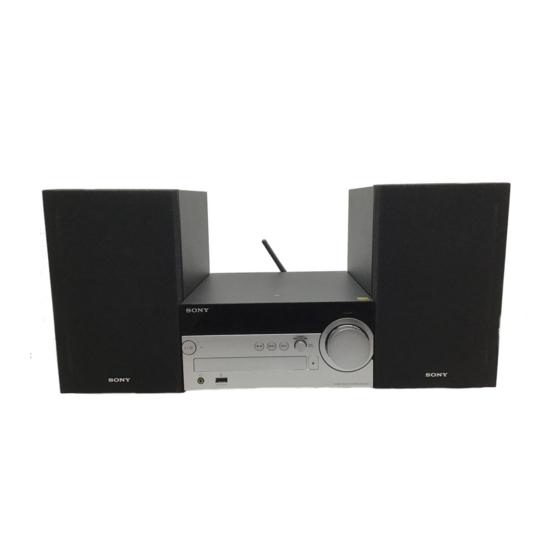
Photo: HCD-SX7B
Model Name Using Similar Mechanism
CD Mechanism Type
Optical Pick-up Block Name
SPECIFICATIONS
BLUETOOTH section
Frequency
Label
Communication system:
187.072 MHz
6D
BLUETOOTH Standard version 3.0
188.928 MHz
7A
Output:
BLUETOOTH Standard Power Class 2
190.640 MHz
7B
Maximum communication range:
192.352 MHz
7C
Line of sight approx. 10 m
194.064 MHz
7D
Frequency band:
2.4 GHz band (2.4000 GHz - 2.4835 GHz)
195.936 MHz
8A
Modulation method:
197.648 MHz
8B
FHSS
199.360 MHz
8C
Compatible BLUETOOTH profiles
A2DP (Advanced Audio Distribution Profile)
201.072 MHz
8D
AVRCP (Audio Video Remote Control Profile)
Supported content protection method
202.928 MHz
9A
SCMS-T method
204.640 MHz
9B
Supported codec
SBC (Sub Band Codec), AAC, LDAC
206.352 MHz
9C
Transmission bandwidth
208.064 MHz
9D
20 Hz – 20,000 Hz (with 44.1 kHz sampling)
209.936 MHz
10A
*
211.648 MHz
10B
213.360 MHz
10C
215.072 MHz
10D
*
216.928 MHz
11A
218.640 MHz
11B
Network section
220.352 MHz
11C
LAN port:
222.064 MHz
11D
RJ-45
10BASE-T/100BASE-TX
223.936 MHz
12A
(The communication speed may vary
depending on the communication
225.648 MHz
12B
environment. This system does not
guarantee the communication speed and
227.360 MHz
12C
quality of 10BASE-T/100BASE-TX.)
229.072 MHz
12D
Wireless LAN:
Compatible standards:
230.784 MHz
13A
IEEE 802.11 a/b/g/n (WEP 64 bit, WEP 128
232.496 MHz
13B
bit)
Frequency band 2.4/5 GHz band
234.208 MHz
13C
WEP 64 bit, WEP 128 bit
WPA/WPA2-PSK (AES)
235.776 MHz
13D
WPA/WPA2-PSK (TKIP)
1
237.488 MHz
13E
Compatible formats:
PCM 192 kHz/24 bit, DSD 2.8 MHz/1 bit
239.200 MHz
13F
DSD (DSF, DSDIFF), LPCM (WAV, AIFF), FLAC,
ALAC, MP3, AAC, WMA
1
*
Frequencies are displayed to two decimal places
on this system.
Canadian Model
Russian Model
Australian Model
HCD-SBT100/SBT100B
CDM90-DVBU204
CMS-S76RFS7G1 or
CMS-S76RFS7GP
General
Power requirements:
Canadian model:
AC 120 V, 60 Hz
Latin America models (except for Argentina
models):
AC 120 V - 240 V, 50 Hz/60 Hz
*1
Other models:
AC 220 V - 240 V, 50 Hz/60 Hz
Power consumption:
46 watts
Dimensions (W/H/D) (incl. projecting parts,
*2
:
without speakers):
Approx. 225 mm x 115 mm x 263 mm
Mass (without speakers):
Approx. 2.7 kg
Design and specifications are subject to
change without notice.
(Type A)
Standby power consumption: 0.5 W (all wireless
network ports off)
1
The actual range will vary depending on factors
Networked Standby mode: 6 W (all wireless
such as obstacles between devices, magnetic
network ports on)
fields around a microwave oven, static
electricity, reception sensitivity, antenna's
(Type B)
performance, operating system, software
application, etc.
Standby power consumption: 0.5 W (all wireless
network ports off)
2
BLUETOOTH standard profiles indicate the
Networked Standby mode: 6 W (all wireless
purpose of BLUETOOTH communication
network ports on)
between devices.
* When the multi-room function turns on, it
supports TDLS (Tunneled Direct Link Setup)
and works as a wireless router that improves
the data communication quality (Version 1.60
or later).
Note: Refer to "TYPE OF AEP
AND UK MODELS" on
page 6 for Type A/B.
COMPACT DISC RECEIVER
E Model
HCD-SX7
AEP Model
UK Model
HCD-SX7/SX7B
HCD-SX7B
SYS SET
Advertisement
Table of Contents

Related Manuals for Sony HCD-SX7


Summary of Contents for Sony HCD-SX7
- Page 1 In case a virus aff ected unit was found during service, contact your Service Headquarters. Photo: HCD-SX7B • HCD-SX7 is the compact disc receiver in CMT-SX7. Model Name Using Similar Mechanism HCD-SBT100/SBT100B • HCD-SX7B is the compact disc receiver in CMT-SX7B.
- Page 2 The BLUETOOTH® word mark and logos are scale. The Simpson 250 and Sanwa SH-63Trd are examples registered trademarks owned by BLUETOOTH SIG, Inc. and any use of such marks by Sony of a passive VOM that is suitable. Nearly all battery operated Corporation is under license.
-
Page 3: Table Of Contents
THESE COMPONENTS WITH SONY PARTS PAR DES PIÈCES SONY DONT LES NUMÉROS SONT DON- WHOSE PART NUMBERS APPEAR AS SHOWN IN THIS NÉS DANS CE MANUEL OU DANS LES SUPPLÉMENTS MANUAL OR IN SUPPLEMENTS PUBLISHED BY SONY. PUBLIÉS PAR SONY. -
Page 4: Servicing Notes
NOTE OF PERFORMING THE OPERATION CHECK IN NOTE OF REPLACING THE TUNER BOARD THE STATE THAT HEAT SINK WAS REMOVED (HCD-SX7 only) When performing the operation check in the state that this unit was When the TUNER board is defective, replace the complete mount- disassembled, it is possible to perform the operation check in the ed board. - Page 5 2020/02/27 22:53:44 (GMT+09:00) HCD-SX7/SX7B NOTE OF REPLACING THE COMPLETE NETWORK CHECKING OF NETWORK CONNECTION BOARD AND CARD WLAN/BT COMBO When replacing the following parts, be sure to carry out the con- When needing to replace the complete NETWORK board or card nection check of network (wired/wireless).
- Page 6 2020/02/27 22:53:44 (GMT+09:00) HCD-SX7/SX7B Ver. 1.3 TEST DISCS TYPE OF AEP AND UK MODELS Use following TEST DISC (for CD) when this unit confi rms the In the AEP and UK models, the MAIN board has been changed in operation and checks it.
- Page 7 2020/02/27 22:53:44 (GMT+09:00) HCD-SX7/SX7B • Please cut out along the dotted line and use it. Note of the MAC address change: Note of the MAC address change: The MAC address of this unit was changed along with this repair. The MAC address of this unit was changed along with this repair.
- Page 8 2020/02/27 22:53:44 (GMT+09:00) HCD-SX7/SX7B MEMO SYS SET...
- Page 9 2020/02/27 22:53:44 (GMT+09:00) HCD-SX7/SX7B • Please cut out along the dotted line and use it. Request of the DLNA re-setup: Request of the DLNA re-setup: The DTCP-IP ID of this unit was changed along with this repair. The DTCP-IP ID of this unit was changed along with this repair.
- Page 10 2020/02/27 22:53:44 (GMT+09:00) HCD-SX7/SX7B MEMO SYS SET...
-
Page 11: Disassembly
2020/02/27 22:53:44 (GMT+09:00) HCD-SX7/SX7B SECTION 2 DISASSEMBLY • This set can be disassembled in the order shown below. 2-1. DISASSEMBLY FLOW 2-2. PANEL (TOP) (Page 12) 2-3. CARD WLAN/BT COMBO 2-4. ANTENNA (2.4 GHz & 5 GHz) (ANT1), 2-5. PANEL (CD) BLOCK... -
Page 12: Panel (Top)
2020/02/27 22:53:44 (GMT+09:00) HCD-SX7/SX7B Note: Follow the disassembly procedure in the numerical order given. 2-2. PANEL (TOP) 1 two screws (BV/ring) (L=8 mm) 2 three screws (BV/ring) (L=8 mm) – – 2 screw Note: Lay a soft piece of cloth under the unit (BV/ring) to avoid damaging the panel (top). -
Page 13: Card Wlan/Bt Combo
2020/02/27 22:53:44 (GMT+09:00) HCD-SX7/SX7B 2-3. CARD WLAN/BT COMBO Note 1: Be sure to replace the complete NETWORK board and card WLAN/ BT combo at the same time. Be sure to also follow “NOTE OF RE- PLACING THE COMPLETE NETWORK BOARD AND CARD WLAN/BT COMBO”... -
Page 14: Antenna (2.4 Ghz & 5 Ghz) (Ant1), Holder (Antenna)
2020/02/27 22:53:44 (GMT+09:00) HCD-SX7/SX7B 2-4. ANTENNA (2.4 GHz & 5 GHz) (ANT1), HOLDER (ANTENNA) Note: When replacing the antenna (Ref. No. ANT1), refer to “CHECK- ING OF NETWORK CONNECTION” on page 5. 3 Move the antenna cable to the rear side. 1 filament tape... -
Page 15: Panel (Cd) Block
2020/02/27 22:53:44 (GMT+09:00) HCD-SX7/SX7B 2-5. PANEL (CD) BLOCK hole – Side view – Insert the clip etc. processed to the length of 8 cm or more in the hole on the side of the chassis and push. 8 cm or more 2 Draw out the tray. -
Page 16: Plate (Top) Block
2020/02/27 22:53:44 (GMT+09:00) HCD-SX7/SX7B 2-6. PLATE (TOP) BLOCK 2 wireless LAN antenna connector (CON4) 1 filament tape (sub material) 3 MAIN board CN606 cable connector cushion (B) filament tape (sub material) Note 1: Check that the wire is not slack. Note 2: Do not connect the wire to the CON5. -
Page 17: Panel (Front) Block-1
2020/02/27 22:53:44 (GMT+09:00) HCD-SX7/SX7B 2-7. PANEL (FRONT) BLOCK-1 • Continued on 2-8 (page 18). 1 two filament tapes (sub material) 7 sleeve ferrite clamp (FC1) 6 filament tape (sub material) 4 USB-HP board CN1501 cable connector (CN605) 5 USB-HP board CN1501 cable connector... -
Page 18: Panel (Front) Block-2
2020/02/27 22:53:44 (GMT+09:00) HCD-SX7/SX7B 2-8. PANEL (FRONT) BLOCK-2 1 screw (BV3 4 Remove the panel (front) block in the direction of the arrow. 6 panel (front) block 3 claw 3 claw 5 Draw the USB-HP board CN1501 4 pin two cables and flexible flat 1 screw cable out of the hole in chassis (sub). -
Page 19: Lcd Module Block
2020/02/27 22:53:44 (GMT+09:00) HCD-SX7/SX7B 2-9. LCD MODULE BLOCK ferrite core (FC2) MAIN board filament tape (sub material) 4 flexible flat cable (6 pin) (CN006) terminal side 3 filament tape (sub material) 1 flexible flat cable 5 ferrite core (FC2) (6 pin) (CN007) -
Page 20: Nfc Module (Nfc1)
2020/02/27 22:53:44 (GMT+09:00) HCD-SX7/SX7B 2-10. NFC MODULE (NFC1) 1 Insert the stick into the hole of the holder (LCD), and lift the NFC module, then peel off the adhesive sheet (NFC) with terminal side a finger. 4 NFC module 3 flexible flat cable... -
Page 21: Bluetooth Module (Bt1)
2020/02/27 22:53:44 (GMT+09:00) HCD-SX7/SX7B 2-12. BLUETOOTH MODULE (BT1) 3 filament tape (sub material) 1 screw filament tape Bluetooth module (BVTP2.6 (sub material) (BT1) 4 flexible flat cable flexible flat cable 5 Bluetooth module (10 pin) (FFC3) (FFC3) (BT1) terminal side 2 Draw out the flexible flat cable (10 pin) (FFC3) from the hole. -
Page 22: Tuner Block (Sx7)
2020/02/27 22:53:44 (GMT+09:00) HCD-SX7/SX7B 2-14. TUNER BLOCK (SX7) 4 tuner block How to install the flexible flat cable When installing the flexible flat cable, ensure that the colored line is parallel to the connector after insertion. Insert at a slant. Insert straight into the interior. -
Page 23: Sheet (Tuner) (Sx7)
2020/02/27 22:53:44 (GMT+09:00) HCD-SX7/SX7B Ver. 1.3 2-16. SHEET (TUNER) (SX7) shield (lower) 5 sheet (tuner) 4 shield (upper) block (inside) notch 6 shield (lower) sheet (tuner) notch 3 cushion (power B) Note: When pasting the cushion (power B), cover the corner of the plate as shown below. -
Page 24: Main Board-1
2020/02/27 22:53:44 (GMT+09:00) HCD-SX7/SX7B 2-18. MAIN BOARD-1 • Continued on 2-19 (page 25). filament tape 0 flexible flat cable (24 pin) (sub material) ferrite core (FC3) (CN503) MAIN board CN010 terminal side qa ferrite core (FC3) 9 filament tape (sub material) 8 flexible flat cable (5 pin) -
Page 25: Main Board-2
2020/02/27 22:53:44 (GMT+09:00) HCD-SX7/SX7B Ver. 1.2 2-19. MAIN BOARD-2 Note 1: When the MAIN board is replaced, refer to “CHECKING Note 2: When replacing the MAIN board of AEP and UK models, be sure OF NETWORK CONNECTION” on page 5. to refer to “TYPE OF AEP AND UK MODELS” on page 6. -
Page 26: Chassis (Sub) Block
2020/02/27 22:53:44 (GMT+09:00) HCD-SX7/SX7B 2-20. CHASSIS (SUB) BLOCK 1 filament tape (sub material) FAN motor cable 4 screw (BV3) filament tape (L=6 mm) chassis (main) (sub material) 4 screw (BV3) chassis (main) (L=6 mm) 2 filament tape (sub material) 3 screw (BV/ring) -
Page 27: Panel (Back) Block, Fan Motor (M1)
2020/02/27 22:53:44 (GMT+09:00) HCD-SX7/SX7B 2-21. PANEL (BACK) BLOCK, FAN MOTOR (M1) Front side – Rear view – 1 screw (BV3) (L=6 mm) 3 Draw the power cord out of the groove. 2 Remove the panel (back) block in the direction of the arrow. -
Page 28: Power Cord (Ac1)
2020/02/27 22:53:44 (GMT+09:00) HCD-SX7/SX7B 2-22. POWER CORD (AC1) Note 1: During reassembly, use new binding band (taiton) to fasten the wires back in place as they were before disassembly. 5 clamp filter (ferrite core) (FC6) 3 power cord connector (CN101) 4 Cut the binding band (taiton). -
Page 29: Power Unit
2020/02/27 22:53:44 (GMT+09:00) HCD-SX7/SX7B 2-23. POWER UNIT sleeve ferrite clamp (FC5) filament tape (sub material) 3 screw (BV3 15 ± 5 mm 5 sheet (PS) to power unit 2 connector (CN205) 3 two screws (CN205) (BV3 3 screw (BV3 1 Remove the wire from the coating clip. -
Page 30: Cd Mechanism Deck Block
2020/02/27 22:53:44 (GMT+09:00) HCD-SX7/SX7B 2-24. CD MECHANISM DECK BLOCK 1 two screws 1 two screws (BV3 (BV3 2 CD mechanism deck block Front side 2-25. FFC HOLDER 1 two filament tapes (sub material) 4 FFC holder Note: When installing the FFC holder, check that installed firmly claw and two bosses. -
Page 31: Optical Pick-Up Block (Cms-S76Rfs7G1/S76Rfs7Gp) (Op1)
2020/02/27 22:53:44 (GMT+09:00) HCD-SX7/SX7B 2-26. OPTICAL PICK-UP BLOCK (CMS-S76RFS7G1/S76RFS7GP) (OP1) 1 two claws 2 chuck holder block 5 insulator screw 0 insulator 5 insulator screw 7 connector qa optical pick-up block (OP1) 0 insulator 5 insulator screw 0 insulator 9 connector Wire... -
Page 32: Test Mode
2020/02/27 22:53:44 (GMT+09:00) HCD-SX7/SX7B Ver. 1.1 SECTION 3 TEST MODE 1. TEST MODE BY THE MAIN UNIT OPERATION 1-3. AM Step Change Mode (SX7: Canadian, Latin It operate the test mode by the main unit. American, Singapore, Argentina, Thai and Indone- sian models) 1-1. - Page 33 2020/02/27 22:53:44 (GMT+09:00) HCD-SX7/SX7B 1-5. RF Mode 3. It enters the common test mode, the message “LINE IN” is displayed on the liquid crystal display. It can turn on or off the wireless signal of WiFi and Bluetooth. (In this mode, “cPLAY” and “SLEEP” continues blinking on...
- Page 34 2020/02/27 22:53:44 (GMT+09:00) HCD-SX7/SX7B Ver. 1.1 2-4. Panel Test Channel setting Channel It can confi rm the liquid crystal display, model name, destination number 2.4 GHz band 5 GHz band and software version. 1 – 13 ch 36 – 165 ch 36 – 116 ch, Procedure: –...
-
Page 35: Electrical Checks
2020/02/27 22:53:44 (GMT+09:00) HCD-SX7/SX7B SECTION 4 ELECTRICAL CHECKS 2-5. Apple Authorization IC Test 2-7. Auto Standby Test 5. Press the [ ] button to close the disc tray. TUNER SECTION 0 dB = 1 V It can confi rm the Apple authorization IC. -
Page 36: Diagrams
2020/02/27 22:53:44 (GMT+09:00) HCD-SX7/SX7B SECTION 5 DIAGRAMS 5-1. BLOCK DIAGRAM - CD/USB Section - OPTICAL PICK-UP BLOCK CMS-S76RFS7G1/ RF AMP, SERVO/AUDIO PROCESSOR MTK-DATAO, CMS-S76RFS7GP IC503 MTK-BCK, MTK-LRCK MTK-DATAO >001B 123 RFIP GPIO MTK-BCK GPIO (Page 38) VOA/A 1 RFC MTK-LRCK GPIO VOB/B... -
Page 37: Block Diagram - Audio Section
2020/02/27 22:53:44 (GMT+09:00) HCD-SX7/SX7B 5-2. BLOCK DIAGRAM - AUDIO Section - I2S_DIN_TD, I2S_BCK_TD, (SX7) I2S_DIN_TD I2S_LRCK_TD >005B (Page 38) WAVE I2S_BCK_TD SHAPER I2S_LRCK_TD IC702, 704 LUTE_I2S_DATA_I, LUTE_I2S_BCK_I, TUNER BOARD LUTE_I2S_DATA_I LUTE_I2S_LRCK_I >006B (Page 38) (SX7B) LUTE_I2S_BCK_I ANTENNA I2S_DATA LUTE_I2S_LRCK_I FM 75 COAXIAL... -
Page 38: Block Diagram - Amp Section
2020/02/27 22:53:44 (GMT+09:00) HCD-SX7/SX7B 5-3. BLOCK DIAGRAM - AMP Section - DIGITAL AUDIO INTERFACE RECEIVER AUDIO DSP, SYSTEM CONTROLLER STREAM PROCESSOR DIGITAL POWER AMP MTK-DATAO, IC204 (3/4) IC1101 IC1104 IC705 MTK-BCK, TB1102 MTK-LRCK MTK-DATAO >001B CN005 10 MPIN4 143 DM1 SSITXD0 24 SDIN1... -
Page 39: Block Diagram - Panel/Power Supply Section
2020/02/27 22:53:44 (GMT+09:00) HCD-SX7/SX7B 5-4. BLOCK DIAGRAM - PANEL/POWER SUPPLY Section - REMOTE CONTROL RECEIVER 10 TIOC4C IC2001 TH001 D905 S2100 56 IRQ7 D912 POWER MONITOR B+ SWITCH Q904 Q905, 906 S2004 D907 135 IRQ2 PROTECT DETECT Q903 D913 D906 S2001 – 2003... - Page 40 2020/02/27 22:53:44 (GMT+09:00) HCD-SX7/SX7B THIS NOTE IS COMMON FOR PRINTED WIRING BOARDS AND SCHEMATIC DIAGRAMS. • Circuit Boards Location (In addition to this, the necessary note is printed in each block.) For Printed Wiring Boards. For Schematic Diagrams. TUNER board (SX7) Note:...
-
Page 41: Schematic Diagram - Main Section (1/9)
2020/02/27 22:53:44 (GMT+09:00) HCD-SX7/SX7B 5-5. SCHEMATIC DIAGRAM - MAIN Section (1/9) - • See page 56 for Waveforms. • See page 56 for IC Block Diagrams. • See page 61 for IC Pin Function Description. MAIN BOARD (1/9) C550 C551 C552 C557 C542 0.01... -
Page 42: Schematic Diagram - Main Section (2/9)
2020/02/27 22:53:44 (GMT+09:00) HCD-SX7/SX7B 5-6. SCHEMATIC DIAGRAM - MAIN Section (2/9) - • See page 56 for IC Block Diagrams. MAIN BOARD (2/9) JL851 >106S FE_3.3V MAIN IC851 BOARD (1/9) (Page 41) +3.3V REGULATOR SL855 SL856 R876 R879 R880 R881 R882 R884... -
Page 43: Schematic Diagram - Main Section (3/9)
2020/02/27 22:53:44 (GMT+09:00) HCD-SX7/SX7B 5-7. SCHEMATIC DIAGRAM - MAIN Section (3/9) - • See page 56 for IC Block Diagrams. MAIN BOARD (3/9) MAIN EVER-5V >116S BOARD D3.3V (9/9) (Page 49) CN006 DP-DI DP-CL CL045 GPIO[0] DP-CE MAIN CL046 FFC3 >117S BOARD... -
Page 44: Schematic Diagram - Main Section (4/9)
2020/02/27 22:53:44 (GMT+09:00) HCD-SX7/SX7B 5-8. SCHEMATIC DIAGRAM - MAIN Section (4/9) - • See page 56 for IC Block Diagrams. MAIN BOARD (4/9) >103S MTK-DP MAIN BOARD MTK-DM (1/9) (Page 41) USB_OC USB_SEL USB_EN NET-CP-SCL NET-CP-SDA LUTE_XRESET JL601 LUTE_WONW_I >124S LUTE_UART_RXD IC605... -
Page 45: Schematic Diagram - Main Section (5/9)
2020/02/27 22:53:44 (GMT+09:00) HCD-SX7/SX7B 5-9. SCHEMATIC DIAGRAM - MAIN Section (5/9) - • See page 56 for IC Block Diagrams. MAIN BOARD (5/9) R314 R321 R328 R335 R342 R356 C211 R265 R266 LUTE_STBY3.3V_EN R267 >121S LUTE_5V_EN R268 LUTE_1.2V_3.3V_EN R269 MAIN LUTE_1.5V_EN BOARD... -
Page 46: Schematic Diagram - Main Section (6/9)
2020/02/27 22:53:44 (GMT+09:00) HCD-SX7/SX7B 5-10. SCHEMATIC DIAGRAM - MAIN Section (6/9) - • See page 56 for Waveforms. • See page 56 for IC Block Diagrams. MAIN BOARD (6/9) >112S (SX7B) I2S_LRCK_TD MAIN R701 47 BOARD I2S_BCK_TD R702 47 (3/9) I2S_DIN_TD (Page 43) -
Page 47: Schematic Diagram - Main Section (7/9)
2020/02/27 22:53:44 (GMT+09:00) HCD-SX7/SX7B 5-11. SCHEMATIC DIAGRAM - MAIN Section (7/9) - • See page 56 for IC Block Diagrams. MAIN BOARD (7/9) >135S AMP+B MAIN IC1106 BOARD POWER-ON (9/9) CL1111 (Page 49) +12V REGULATOR CL1112 IC1106 XC6701BC02PR-G CL1129 IC1102 11.8 25.6 VOUT +3.3V REGULATOR... -
Page 48: Schematic Diagram - Main Section (8/9)
2020/02/27 22:53:44 (GMT+09:00) HCD-SX7/SX7B Ver. 1.2 5-12. SCHEMATIC DIAGRAM - MAIN Section (8/9) - • See page 56 for Waveforms. • See page 56 for IC Block Diagrams. • See page 61 for IC Pin Function Description. (NC) MAIN (Page 45) >131S... -
Page 49: Schematic Diagram - Main Section (9/9)
2020/02/27 22:53:44 (GMT+09:00) HCD-SX7/SX7B 5-13. SCHEMATIC DIAGRAM - MAIN Section (9/9) - • See page 56 for Waveforms. • See page 56 for IC Block Diagrams. MAIN BOARD (9/9) >135S MAIN AMP+B BOARD POWER-ON (7/9) D910 R940 (Page 47) DA2J10100L D905 >109S... -
Page 50: Printed Wiring Boards - Main Section (1/2) (Former Type)
2020/02/27 22:53:44 (GMT+09:00) HCD-SX7/SX7B 5-14. PRINTED WIRING BOARDS - MAIN Section (1/2) (Former type) - • See page 40 for Circuit Boards Location. • : Uses unleaded solder. (FAN) NETWORK (Page 54) USB-HP BOARD BOARD >04P MAIN BOARD (NC) CN1501 (SIDE A) -
Page 51: Printed Wiring Boards - Main Section (2/2) (Former Type)
2020/02/27 22:53:44 (GMT+09:00) HCD-SX7/SX7B Ver. 1.1 5-15. PRINTED WIRING BOARDS - MAIN Section (2/2) (Former type) - • See page 40 for Circuit Boards Location. • : Uses unleaded solder. J001 SPEAKERS INPEDANCE USE 6 LINE IN OPTICAL IN TB1101 – –... -
Page 52: Printed Wiring Boards - Main Section (1/2) (New Type)
2020/02/27 22:53:44 (GMT+09:00) HCD-SX7/SX7B 5-16. PRINTED WIRING BOARDS - MAIN Section (1/2) (New type) - • See page 40 for Circuit Boards Location. • : Uses unleaded solder. (FAN) NETWORK (Page 54) USB-HP BOARD BOARD >08P MAIN BOARD (NC) CN1501 (SIDE A) -
Page 53: Printed Wiring Boards - Main Section (2/2) (New Type)
2020/02/27 22:53:44 (GMT+09:00) HCD-SX7/SX7B Ver. 1.2 5-17. PRINTED WIRING BOARDS - MAIN Section (2/2) (New type) - • See page 40 for Circuit Boards Location. • : Uses unleaded solder. J001 SPEAKERS INPEDANCE USE 6 LINE IN OPTICAL IN TB1101 – –... -
Page 54: Printed Wiring Boards - Panel Section
2020/02/27 22:53:44 (GMT+09:00) HCD-SX7/SX7B 5-18. PRINTED WIRING BOARDS - PANEL Section - • See page 40 for Circuit Boards Location. • : Uses unleaded solder. Former type (Suffix-11) J1500 POWER-KEY BOARD USB-HP BOARD FRONT BOARD R1505 D2100 (Page 50) JL1500 ON/STANDBY C1502... -
Page 55: Schematic Diagram - Panel Section
2020/02/27 22:53:44 (GMT+09:00) HCD-SX7/SX7B 5-19. SCHEMATIC DIAGRAM - PANEL Section - FRONT BOARD POWER-KEY BOARD Q2100 Q2101 CN2001 CN2100 LTA014EUBFS8TL LTA014EUBFS8TL LED DRIVE LED DRIVE CL2100 EVER3.3V CL2101 GREEN CL2102 POWER POWER CN2002 CL2103 GREEN CL2001 CL2104 CL2105 CL2106 EVER3.3V CL2002 KEY1... - Page 56 2020/02/27 22:53:44 (GMT+09:00) HCD-SX7/SX7B • Waveforms • IC Block Diagrams IC201 TCA6424ARGJR – MAIN Board – – MAIN Board – IC003, 606, 608 MM3411A33URE GND 25 IC503 8 (XTALO) IC705 ea (XOUT) IC204 os (AUDIO_X2) IC501 MM3411A12URE ADDR 26 IC907, 1102 MM3571A33URE...
- Page 57 2020/02/27 22:53:44 (GMT+09:00) HCD-SX7/SX7B IC605 TPS2560DRCR IC607 BD11600NUX-E2 GND 1 CURRENT IN 2 SENSE IN 3 1D+ 1 10 FAULT1 THERMAL 1D– 2 D– SENSE 9 OUT1 CHARGE 9-ms PUMP DEGLITCH 8 OUT2 2D+ 3 EN1 4 CURRENT DRIVER 7 ILLM 2D– 4...
- Page 58 2020/02/27 22:53:44 (GMT+09:00) HCD-SX7/SX7B IC705 LC89075WA-H 62 61 60 59 58 57 56 RXIN5 RXIN6 RXIN7 RXIN8 MUX 15:3 GROUP: C S/PDIF GROUP: D LPF 1 DIGITAL INTERFACE RECEIVER PGND 2 MASTER CLOCK MCKIN 3 BIT CLOCK BCKIN 4 LR CLOCK or DSD...
- Page 59 2020/02/27 22:53:44 (GMT+09:00) HCD-SX7/SX7B IC902 – 904 TPS54332CDDAR 8 PH 7 GND BOOT MAXIMUM BOOT 1 UNDERVOLTAGE 6 COMP CLAMP LOCKOUT BOOT THERMAL CHARGE SHUTDOWN DISCHARGE LOGIC ECO-MODE VIN 2 MINIMUM CLAMP ENABLE COMPARATOR SHUTDOWN VOLTAGE ENABLE THRESHOLD LOGIC LATCH REFERENCE GATE...
- Page 60 2020/02/27 22:53:44 (GMT+09:00) HCD-SX7/SX7B IC1104 TAS5624ADDVR GVDD_AB 1 BST_A BST_B VDD 2 OC_ADJ 3 RESET 4 OUT_A ANALOG PWM & TIMING GATE- LOOP FILTER CONTROL DRIVE INPUT_A 5 – OUT_A RECEIVER PVDD_AB PVDD_AB PVDD_AB INPUT_B 6 ANALOG PWM & TIMING GATE- RECEIVER...
- Page 61 USB VBUS power over current detection signal input terminal PVCC Power supply terminal (+3.3V) RDS interrupt signal input from the TUNER board (HCD-SX7) P6_5 +3.3V power on/off control signal output to the DAB board for the DAB tuner section “H”: power on (HCD-SX7B)
- Page 62 2020/02/27 22:53:44 (GMT+09:00) HCD-SX7/SX7B Pin No. Pin Name Description Power on/off control signal output to the TUNER board for the tuner section “H”: power on (HCD-SX7) P7_10 +1.2V power on/off control signal output to the DAB board for the DAB tuner section “H”: power on (HCD-SX7B)
- Page 63 Two-way I2C clock signal bus with the MFI SDA0 Two-way I2C data bus with the MFI Two-way I2C clock signal bus with the TUNER board and NFC module (HCD-SX7) SCL1 Two-way I2C clock signal bus with the NFC module (HCD-SX7B)
- Page 64 2020/02/27 22:53:44 (GMT+09:00) HCD-SX7/SX7B Pin No. Pin Name Description Ground terminal SPBIO10_0 Serial data input from the serial fl ash P5_0 Power on/off control signal output terminal “H”: power on PVCC Power supply terminal (+3.3V) P5_1 Reset signal output to the I/O expander “L”: reset...
- Page 65 2020/02/27 22:53:44 (GMT+09:00) HCD-SX7/SX7B MAIN BOARD IC503 CXD90013R (RF AMP, SERVO/AUDIO PROCESSOR) Pin No. Pin Name Description RF main beam (A) input from the optical pick-up block RF main beam (D) input from the optical pick-up block RF sub beam (F) input from the optical pick-up block...
- Page 66 2020/02/27 22:53:44 (GMT+09:00) HCD-SX7/SX7B Pin No. Pin Name Description DVSS12 Ground terminal (digital system) Column address strobe signal output to the SD-RAM Row address strobe signal output to the SD-RAM DVDD33_84 Power supply terminal (+3.3V) (digital system) 85, 86 BA0, BA1 Bank address signal output to the SD-RAM DVDD12_87 Power supply terminal (+1.2V) (digital system)
-
Page 67: Exploded Views
2020/02/27 22:53:44 (GMT+09:00) HCD-SX7/SX7B SECTION 6 EXPLODED VIEWS Note: • -XX and -X mean standardized parts, so • The mechanical parts with no reference The components identifi ed by mark 0 they may have some difference from the number in the exploded views are not sup- or dotted line with mark 0 are critical for original one. -
Page 68: Base (Cd) Section
2020/02/27 22:53:44 (GMT+09:00) HCD-SX7/SX7B Ver. 1.1 6-2. BASE (CD) SECTION not supplied card WLAN/BT combo not supplied not supplied not supplied not supplied not supplied NETWORK board ANT1 supplied not supplied Note 1: Be sure to replace the NETWORK board and card WLAN/BT combo at the same time. Be sure to also follow “NOTE OF REPLACING THE... -
Page 69: Front Panel Section
2020/02/27 22:53:44 (GMT+09:00) HCD-SX7/SX7B 6-3. FRONT PANEL SECTION • Rear view supplied with EN2001 FFC1 not supplied (FRONT board) EN2001 not supplied not supplied not supplied (POWER-KEY board) not supplied (USB-HP board) not supplied not supplied Ref. No. Part No. Description Remark Ref. -
Page 70: Main Board Section
2020/02/27 22:53:44 (GMT+09:00) HCD-SX7/SX7B Ver. 1.3 6-4. MAIN BOARD SECTION CN01 153 153 152 152 DAB1 (See Note 4) not supplied FFC7 (SX7B) (SX7) Note 1: This part is deleted from the midway of production. (SX7) – Rear view – not supplied... -
Page 71: Lcd Module Section
2020/02/27 22:53:44 (GMT+09:00) HCD-SX7/SX7B Ver. 1.2 6-5. LCD MODULE SECTION not supplied not supplied not supplied FFC3 NFC1 not supplied FFC4 not supplied LCD1 chassis section Ref. No. Part No. Description Remark Ref. No. Part No. Description Remark 3-077-331-21 +BV3 (3-CR) (L = 6 mm) -
Page 72: Chassis Section
2020/02/27 22:53:44 (GMT+09:00) HCD-SX7/SX7B Ver. 1.2 6-6. CHASSIS SECTION CD mechanism deck section (CDM90-DVBU204) not supplied not supplied not supplied not supplied not supplied not supplied not supplied Ref. No. Part No. Description Remark Ref. No. Part No. Description Remark 3-077-331-21 +BV3 (3-CR) (L = 6 mm) -
Page 73: Cd Mechanism Deck Section
2020/02/27 22:53:44 (GMT+09:00) HCD-SX7/SX7B 6-7. CD MECHANISM DECK SECTION (CDM90-DVBU204) not supplied CDM1 not supplied not supplied MS-476 not supplied board FFC6 FFC5 Ref. No. Part No. Description Remark Ref. No. Part No. Description Remark 2-634-618-21 INSULATOR FFC6 9-885-201-78 FY15 FFC (1.0 mm 5P CDM) -
Page 74: Electrical Parts List
2020/02/27 22:53:44 (GMT+09:00) HCD-SX7/SX7B Ver. 1.2 SECTION 7 FRONT MAIN ELECTRICAL PARTS LIST Note: When indicating parts by reference num- • Due to standardization, replacements in • CAPACITORS ber, please include the board name. the parts list may be different from the uF: μF... - Page 75 2020/02/27 22:53:44 (GMT+09:00) HCD-SX7/SX7B MAIN Ref. No. Part No. Description Remark Ref. No. Part No. Description Remark C025 1-118-388-11 CERAMIC CHIP 0.047uF C252 1-164-858-11 CERAMIC CHIP 22PF C026 1-116-344-11 ELECT CHIP 330uF 6.3V C254 1-119-751-11 TANTALUM CHIP 22uF C035 1-116-737-11 CERAMIC CHIP 1uF...
- Page 76 2020/02/27 22:53:44 (GMT+09:00) HCD-SX7/SX7B MAIN Ref. No. Part No. Description Remark Ref. No. Part No. Description Remark C561 1-118-459-11 CERAMIC CHIP 0.01uF C709 1-118-417-11 CERAMIC CHIP 0.1uF C562 1-118-459-11 CERAMIC CHIP 0.01uF C712 1-118-386-11 CERAMIC CHIP 0.1uF 16V (SX7) C563 1-116-708-11 CERAMIC CHIP 47uF 6.3V...
- Page 77 2020/02/27 22:53:44 (GMT+09:00) HCD-SX7/SX7B MAIN Ref. No. Part No. Description Remark Ref. No. Part No. Description Remark * C925 1-116-714-11 CERAMIC CHIP 22uF 6.3V C1135 1-164-874-11 CERAMIC CHIP 100PF * C926 1-116-714-11 CERAMIC CHIP 22uF 6.3V C1136 1-118-386-11 CERAMIC CHIP 0.1uF C927...
- Page 78 2020/02/27 22:53:44 (GMT+09:00) HCD-SX7/SX7B MAIN Ref. No. Part No. Description Remark Ref. No. Part No. Description Remark C1208 1-118-375-11 CERAMIC CHIP 0.0068uF FB003 1-481-746-11 SDM EMI FERRITE (SX7) C1209 1-118-375-11 CERAMIC CHIP 0.0068uF FB007 1-481-746-11 SDM EMI FERRITE (SX7) C1210 1-118-375-11 CERAMIC CHIP 0.0068uF...
- Page 79 2020/02/27 22:53:44 (GMT+09:00) HCD-SX7/SX7B MAIN Ref. No. Part No. Description Remark Ref. No. Part No. Description Remark IC1102 6-719-722-01 IC MM3571A33URE < RESISTOR/FERRITE BEAD > IC1103 8-759-422-21 IC NJM4580V (TE2) IC1104 6-721-021-01 IC TAS5624ADDVR R002 1-218-989-11 METAL CHIP 1/16W IC1106 6-721-044-01 IC XC6701BC02PR-G...
- Page 80 2020/02/27 22:53:44 (GMT+09:00) HCD-SX7/SX7B MAIN Ref. No. Part No. Description Remark Ref. No. Part No. Description Remark R247 1-218-941-81 METAL CHIP 1/16W R321 1-218-965-11 METAL CHIP 1/16W R248 1-218-941-81 METAL CHIP 1/16W R324 1-218-965-11 METAL CHIP 1/16W R249 1-400-823-11 EMI FERRITE (SMD) (1005)
- Page 81 2020/02/27 22:53:44 (GMT+09:00) HCD-SX7/SX7B Ver. 1.2 MAIN Ref. No. Part No. Description Remark Ref. No. Part No. Description Remark R424 1-218-965-11 METAL CHIP 1/16W R491 1-218-961-11 METAL CHIP 4.7K 1/16W R425 1-218-965-11 METAL CHIP 1/16W R426 1-216-821-11 METAL CHIP 1/10W R492 1-218-961-11 METAL CHIP 4.7K...
- Page 82 2020/02/27 22:53:44 (GMT+09:00) HCD-SX7/SX7B MAIN Ref. No. Part No. Description Remark Ref. No. Part No. Description Remark R607 1-218-941-81 METAL CHIP 1/16W R725 1-218-941-81 METAL CHIP 1/16W R608 1-218-941-81 METAL CHIP 1/16W R726 1-218-941-81 METAL CHIP 1/16W R610 1-218-941-81 METAL CHIP 1/16W...
- Page 83 2020/02/27 22:53:44 (GMT+09:00) HCD-SX7/SX7B MAIN Ref. No. Part No. Description Remark Ref. No. Part No. Description Remark R927 1-208-911-11 METAL CHIP 0.5% 1/16W R1133 1-216-833-11 METAL CHIP 1/10W R928 1-208-671-11 METAL CHIP 0.5% 1/16W R1134 1-216-833-11 METAL CHIP 1/10W R929 1-208-855-81 METAL CHIP 0.5%...
- Page 84 2020/02/27 22:53:44 (GMT+09:00) HCD-SX7/SX7B Ver. 1.3 MAIN MS-476 NETWORK POWER-KEY TUNER USB-HP Ref. No. Part No. Description Remark Ref. No. Part No. Description Remark < VIBRATOR > Q2101 6-552-922-01 TRANSISTOR LTA014EUBFS8TL X201 1-814-485-11 QUARTZ CRYSTAL UNIT (48 MHz) < RESISTOR > X202 1-814-835-11 QUARTZ CRYSTAL UNIT (24.576 MHz)
- Page 85 2020/02/27 22:53:44 (GMT+09:00) HCD-SX7/SX7B Ver. 1.2 Ref. No. Part No. Description Remark 1-500-082-11 CLAMP, SLEEVE FERRITE 1-481-359-11 CORE, FERRITE 1-469-829-11 CORE, FERRITE 1-500-635-11 CORE, FERRITE * FC5 1-500-082-11 CLAMP, SLEEVE FERRITE 1-481-529-21 FILTER, CLAMP (FERRITE CORE) FFC1 9-885-201-77 FY15 FFC (1.0 mm 11P FRONT)
- Page 86 Ver. Date Description of Revision 2015.06 2015.07 Addition of Russian, Latin American, Singapore, Argentina, Thai and Indonesian models (HCD-SX7) Deletion of “THE USER REGISTRATION DELETION METHOD OF SEN SERVICE” (SMR-15014) 2017.01 Change of MAIN board (AEP and UK models) Change of Part No. for LCD MODULE (Ref. No. LCD1) Change of Part No.
Need help?
Do you have a question about the HCD-SX7 and is the answer not in the manual?
Questions and answers
turntable setup. LINE IN?
To set up a turntable with the Sony HCD-SX7 using LINE IN:
1. Connect the turntable’s audio output cables (usually RCA) to the LINE IN jacks on the back of the HCD-SX7.
2. Make sure the turntable has a built-in phono preamp or use an external one, as LINE IN requires line-level signal.
3. Set the HCD-SX7 to the LINE IN input mode to play audio from the turntable.
Ensure proper grounding if needed to avoid hum.
This answer is automatically generated