Table of Contents
Advertisement
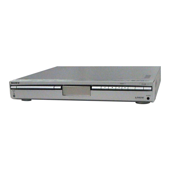
SERVICE MANUAL
Ver 1.0 2004.06
HCD-SB500W is the amplifier, super audio CD/DVD
system and tuner section in DAV-SB500W.
Amplifier section
Stereo mode (rated)
65 W+65 W (4 ohms at
1 kHz, DIN)
Surround mode (reference)
Front: 96 W+96 W
(with SS-TS11)
Center: 96 W
(with SS-CT11)
Subwoofer: 170 W
(with SS-WS11)
* Depending on the sound field settings and the source,
there may be no sound output.
Inputs
VIDEO (AUDIO IN):
Sensitivity: 250 mV
Impedance: 50 kilohms
SAT (AUDIO IN):
Sensitivity: 450 mV
Impedance: 50 kilohms
Phones
Accepts low-and high-
impedance headphones.
Super Audio CD/DVD system
Laser
Semiconductor laser
(S
uper Audio CD/DVD:
λ = 650 nm)
(CD: λ = 780 nm)
Emission duration:
continuous
Signal format system
NTSC or NTSC/PAL
Frequency response (at 2 CH STEREO mode)
DVD (PCM): 2 Hz to 22
kHz (±1.0 dB)
CD: 2 Hz to 20 kHz (±1.0
dB)
Sony Corporation
9-879-015-01
Home Audio Company
2004F05-1
Published by Sony Engineering Corporation
© 2004.06
HCD-SB500W
Model Name Using Similar Mechanism
Mechanism Type
Optical Traverse Unit Name
SPECIFICATIONS
Tuner section
System
PLL quartz-locked digital
synthesizer system
FM tuner section
87.5 − 108.0 MHz (50 kHz
Tuning range
step)
antenna (aerial)
FM wire antenna (aerial)
antenna (aerial) terminals 75 ohms, unbalanced
Intermediate frequency
10.7 MHz
AM tuner section
531 − 1,602 kHz (with the
Tuning range
interval set at 9 kHz)
530 − 1,710 kHz (with the
interval set at 10 kHz)
antenna (aerial)
AM loop antenna (aerial)
Intermediate frequency
450 Hz
Video section (exept AEP, UK models)
Outputs
Video: Vp-p 75 ohms
S video:
Y: 1 Vp-p 75 ohms
C: 0.286 Vp-p 75 ohms
COMPONENT:
Y: 1 Vp-p 75 ohms
P
/C
, P
/C
B
B
R
75 ohms
Video section (EURO AV) (AEP,UK models)
Outputs
Video: 1 Vp-p 75 ohms
SUPER AUDIO CD/DVD RECEIVER
Australian Model
General
System
Power requirements
Power consumption
Dimensions (approx.)
Mass (approx.)
Design and specifications are subject to change
without notice.
: 0.7 Vp-p
R
AEP Model
UK Model
E Model
NEW
CDM77A-DVBU20
DBU-1
220 − 240 V AC, 50/60 Hz
90 W (220-240 V AC)
0.3 W (220-240 V AC) ( at
the Power Saving Mode)
430 × 70 × 393 mm
(w/h/d) incl. projecting
parts
4.4 kg
Advertisement
Table of Contents

Related Manuals for Sony HCD-SB500W


Summary of Contents for Sony HCD-SB500W
- Page 1 HCD-SB500W SERVICE MANUAL AEP Model UK Model Ver 1.0 2004.06 E Model Australian Model HCD-SB500W is the amplifier, super audio CD/DVD system and tuner section in DAV-SB500W. Model Name Using Similar Mechanism Mechanism Type CDM77A-DVBU20 Optical Traverse Unit Name DBU-1...
- Page 2 COMPONENTS IDENTIFIED BY MARK 0 OR DOTTED LINE WITH MARK 0 ON THE SCHEMATIC DIAGRAMS AND IN THE PARTS LIST ARE CRITICAL TO SAFE OPERATION. REPLACE THESE COMPONENTS WITH SONY PARTS WHOSE PART NUMBERS APPEAR AS SHOWN IN THIS MANUAL OR IN SUPPLEMENTS PUBLISHED BY SONY.
- Page 3 HCD-SB500W Disc Examples of discs that the system Copyrights Title cannot play structure This product incorporates copyright protection Chapter technology that is protected by U.S. patents and The system cannot play the following discs: Disc other intellectual property rights. Use of this •...
-
Page 4: Table Of Contents
HCD-SB500W TABLE OF CONTENTS SERVICING NOTES 6-39. Printed Wiring Boards – POWER SUPPLY Section ..64 ..........5 6-40. Schematic Diagarm – POWER SUPPLY Section – ..65 GENERAL ..............7 EXPLODED VIEWS 7-1. Front Panel Section ............87 DISASSEMBLY 7-2. -
Page 5: Servicing Notes
HCD-SB500W SECTION 1 SERVICING NOTES • MODEL IDENTIFICATION NOTES ON HANDLING THE OPTICAL PICK-UP BLOCK OR BASE UNIT – Back Panel – The laser diode in the optical pick-up block may suffer electrostatic break-down because of the potential difference generated by the charged electrostatic load, etc. - Page 6 HCD-SB500W DECISION TO PASS OR FAIL OF THE OPTICAL PICK-UP BLOCK Connection: oscilloscope DMB07 board CN901 1 pin – CN901 3 pin Procedure: 1. Connect an oscilloscope to test point 1 pin and 3 pin of CN901 on the DMB07 board.
-
Page 7: General
HCD-SB500W SECTION 2 This section is extracted from instruction manual. GENERAL Front Panel PRESET VOLUME FUNCTION STANDBY PHONES A "/1 (power) H FUNCTION B Disc tray I VOLUME –/+ C A (open/close) J PHONES jack D H (play) K Front panel display... - Page 8 HCD-SB500W A SONY TV DIRECT Remote B SLEEP C TUNER/BAND D MUTING E TUNER MENU F PLAY MODE G REPEAT H FM MODE I TV J AUDIO K ANGLE L SUBTITLE M ./>, PRESET –/+ N H PLAY O X PAUSE P DVD TOP MENU/ALBUM–...
-
Page 9: Disassembly Flow
HCD-SB500W SECTION 3 DISASSEMBLY • This set can be disassembled in the order shown below. 3-1. DISASSEMBLY FLOW 3-2. CASE (Page 9) 3-3. FRONT PANEL BLOCK 3-4. DVD MECHANISM DECK 3-5. IO BOARD (Page 10) (Page 10) (Page 11) 3-7. TRAY (AU) 3-10. -
Page 10: Front Panel Block
HCD-SB500W 3-3. FRONT PANEL BLOCK 2 four screws × 8) (DIA.2.6 5 claw 1 wire (flat type) (17 core) (CN503) 8 front panel 3 screw block ( BV3) 5 claw 7 connector (CN04) 4 four screws (BV3) 3-4. DVD MECHANISM DECK... -
Page 11: Io Board
HCD-SB500W 3-5. IO BOARD • Abbreviation RU: Russian model 5 I/O board × 8) 2 screw (DIA.2.6 (except AEP, UK, RU) 4 wire (flat type) (11 core) (CN200) 2 two screws (BV3) (AEP, UK, RU) 2 two screws (except AEP, UK, RU) -
Page 12: Tray (Au)
HCD-SB500W 3-7. TRAY (AU) 1 Slide the chuck cam in the direction of arrow A . 3 claw 3 claw 4 tray (AU) 3-8. OPTICAL PICK-UP BLOCK, CHUCK CAM 2 support 3 belt 9 chuck cam 1 claw 5 pulley... -
Page 13: Optical Traverse Unit (Dbu-1)
HCD-SB500W 3-9. OPTICAL TRAVERSE UNIT (DBU-1) 6 holder (DBU1) 1 claw 7 insulator 7 insulator 3 w ire (flat type) (24 core) (CN001) 5 step screw (M) 5 step screw (M) 7 insulator 2 flexible board (CN003) 8 optical traverse unit... -
Page 14: Test Mode
HCD-SB500W SECTION 4 TEST MODE COLD RESET KEY TEST The cold reset clears all data including preset data stored in the This mode is used to check the front panel keys. RAM to initial conditions. Execute this mode when returning the... - Page 15 HCD-SB500W DVD DEBUG MODE DVD SECTION This mode is used to unable to reset for performing the debug of DVD. DVD TEST MODE GENERAL DESCRIPTION Procedure: The Test Mode allows you to make diagnosis and adjustment easily 1. Press the button to turn the power on.
- Page 16 HCD-SB500W OPERATING DVD TEST MODE General Description of Checking Method Selecting 2 and subsequent items calls the submenu screen of each item. And selecting 2 and subsequent items executes respective 0. Syscon Diagnosis menus and outputs the results. The same contents as board detail check by serial interface can be For the contents of each submenu, see “Check Items List”...
- Page 17 HCD-SB500W 1. Drive Auto Adjustment 1-1. DVD-SL (single layer) Press the [1] key on the remote commander and insert a DVD single On the Test Mode Menu screen, press the [1] key on the remote layer disc following the message. Then the adjustment will be made commander, and the Adjustment Menu will be displayed.
- Page 18 HCD-SB500W 1-3. DVD-DL (dual layer) 2. Drive Manual Operation Press the [3] key on the remote commander and insert a DVD dual Note: This mode is used for design, and not used in service fundamentally. layer disc following the message. Then the adjustment will be made...
- Page 19 HCD-SB500W 2-1. Disc Type 2-1-3. Disc Type CD It sets up so that it may judge as a disc type of specification of the disc with which the set was inserted. Disc Type [1]: CD disc (normal speed, 12 cm)
- Page 20 HCD-SB500W 2-3. Track/Layer Jump 2-5. EEPROM Write Adjust Track/Layer Jump EEPROM Write Adjust FWD R.Lj L0>L1 REV L.Lj L1>L0 1. Focus Offset 3.500Tj Fine FWD U.Fj L0>L1 2. Focus Gain 4.500Tj Fine REV D.Fj L1>L0 3. Trk. Offset Coarse 5.10kTj Dirc 4.
- Page 21 HCD-SB500W 2-7. Disc Check Memory 3. Mecha Aging On the Test Mode Menu screen, selecting [3] executes the aging of Disc Check Memory the mechanism deck. 1. SL Disc check ### Aging Test MENU ### 2. CD Disc check ** Pls use over 40min.CD ** 3.
- Page 22 HCD-SB500W 4. Emergency History 5. Mecha Error History On the Test Mode Menu screen, selecting [4] displays the On the Test Mode Menu screen, selecting [5] displays the information such as servo emergency history. information of mechanism deck error history.
-
Page 23: Electrical Adjustments
HCD-SB500W SECTION 5 ELECTRICAL ADJUSTMENTS cc : Operating status of table at an error occurred. About the dicision to pass or fail of the optical pick-up block, (tbl sq jcp) refer to “DICISION TO PASS OR FAIL OF THE OPTICAL PICK- : The rotation stop position determination error UP BLOCK”... -
Page 24: Block Diagram - Rf Servo Section
HCD-SB500W SECTION 6 DIAGRAMS 6-1. BLOCK DIAGRAM – RF SERVO Section – • SIGNAL PATH RF_AC : AUDIO : CD PLAY (Page 26) : DVD PLAY : VIDEO : SACD PLAY 117 RFIN SD0 – SD7 DVDRFP ATOP (Page 25) -
Page 25: Block Diagram - Dvd Dsp Section
HCD-SB500W 6-2. BLOCK DIAGRAM – DVD DSP Section – AV0 - AV7 (Page 26) • R-ch is omitted due to same as L-ch. XSAK#, SDEF#, XDCK#, XSHD# • SIGNAL PATH (Page 26) : AUDIO : COMPONENT VIDEO : VIDEO : R, G, B DATA1 –... -
Page 26: Block Diagram - Audio Section
HCD-SB500W 6-3. BLOCK DIAGRAM – AUDIO Section – RF_AC (Page 24) 126 WARFI DSAL 39 DSIFL D1, D3, SCK, BCKO, LRCKO DSAR 40 DSIFR (Page 27) POFLR (Page 24) 123 WCK POCSW 41 DSICT DSAC POSLR DSALFE 42 DSISW LRCKO... -
Page 27: Block Diagram - Amp, Panel Section
HCD-SB500W 6-4. BLOCK DIAGRAM – AMP, PANEL Section – IC108 STREAM PROCESSOR J800 HPOUTL1 PHONES HPOUTL2 IC301 • SIGNAL PATH HEADPHONE HPOUTR1 Q505 Q800, 801, : AUDIO Q803, 804, MUTING HPOUTR2 MUTING CONTROL TB301 IC101 SPEAKER POWER DRIVER D1, D3, SCK,... -
Page 28: Block Diagram - Power Supply Section
HCD-SB500W 6-5. BLOCK DIAGRAM – POWER SUPPLY Section – SWITCHING IC801 REGULATOR TX 2.5V +2.5V REGULATOR IC900 TX 9V VCC (TRANSMIT) REGULATOR IC303 AMP 1.8V +1.8V REGULATOR AMP 3.3V 3.3V (AMP) AMP 12V, FAN 12V 12V (AMP) 29.5V 29.5V (AMP) - Page 29 HCD-SB500W • Note for Printed Wiring Boards and Schematic Diagrams • Circuit Boards Location Note on Printed Wiring Board: Note on Schematic Diagram: • X : parts extracted from the component side. • All capacitors are in µF unless otherwise noted. (p: pF) DIAT TRASMIT board •...
-
Page 30: Printed Wiring Board - Rf Board
HCD-SB500W • See page 29 for Circuit Boards Location. 6-6. PRINTED WIRING BOARD – RF Board – :Uses unleaded solder. RF BOARD RF BOARD (COMPONENT SIDE) (CONDUCTOR SIDE) R041 C003 C001 Q002 R009 OPTICAL R008 TRAVERSE L002 UNIT R007 R005... -
Page 31: Schematic Diagram - Rf Board
HCD-SB500W • See page 66 for IC Block Diagram. • See page 43 for Waveforms. 6-7. SCHEMATIC DIAGRAM – RF Board – RFMON C006 C028 C027 R026 C013 CN002 C030 0.01 C026 AGND C025 R023 C029 RFAC 0.01 C024 C035... -
Page 32: Printed Wiring Board - Dmb07 Board (Component Side)
HCD-SB500W • See page 29 for Circuit Boards Location. 6-8. PRINTED WIRING BOARD – DMB07 Board (Component Side) – : Uses unleaded solder. MAIN BOARD IO BOARD CN505 CN202 (Page 56) DMB07 BOARD (Page 44) (COMPONENT SIDE) CN101 CN105 C924... -
Page 33: Printed Wiring Board - Dmb07 Board (Conductor Side)
HCD-SB500W • See page 29 for Circuit Boards Location. : Uses unleaded solder. 6-9. PRINTED WIRING BOARD – DMB07 Board (Conductor Side) – DMB07 BOARD (CONDUCTOR SIDE) R282 R281 R201 R280 R279 R278 R293 IC352 C817 C839 R329 R220 R328... -
Page 34: Schematic Diagram - Dmb07 Board (1/9)
HCD-SB500W • See page 66 for IC Block Diagram. • See page 43 for Waveforms. 6-10. SCHEMATIC DIAGRAM – DMB07 Board (1/9) – (1/9) C518 0.01 FL502 C517 C545 C543 C567 C568 0.01 0.01 C522 R537 R536 WAVRB IC503 NJM3404AV(TE2) -
Page 35: Schematic Diagram - Dmb07 Board (2/9)
HCD-SB500W • See page 72 for IC Pin Function Description. 6-11. SCHEMATIC DIAGRAM – DMB07 Board (2/9) – (2/9) ANALOG_BUS R787 R786 R785 100k 100k C782 IC703(2/2) 0.0015 NJM3404AV(TE2) R788 R700 C715 (1/2) MDIN 100k 8.2k 0.0015 COMPARATOR FL706 C783 R789 0.0015... -
Page 36: Schematic Diagram - Dmb07 Board (3/9)
HCD-SB500W • See page 72 for IC Pin Function Description. 6-12. SCHEMATIC DIAGRAM – DMB07 Board (3/9) – (3/9) FL811 WAVRB C858 R804 C860 C861 C855 0.01 0.01 0.01 R874 C863 ANALOG_BUS R870 R842 C865 C866 (Page 35) 0.01 0.01 DGND +2.5V REGULATOR... -
Page 37: Schematic Diagram - Dmb07 Board (4/9)
HCD-SB500W • See page 66 for IC Block Diagrams. 6-13. SCHEMATIC DIAGRAM – DMB07 Board (4/9) – (4/9) DSMCK2 C825 C824 R813 0.01 0.01 ZIVA_5.1CH_BUS (Page 41) R858 DSBC R854 FLR-A DSFL R853 CSW-A CN106 DSFR R847 SLR-A DGND DSCT... -
Page 38: Schematic Diagram - Dmb07 Board (5/9)
HCD-SB500W 6-14. SCHEMATIC DIAGRAM – DMB07 Board (5/9) – (Page 34) (5/9) (Page 40) DGND A3V-2 (Page 41) C526 C527 VGND 0.01 (Page 41) R589 R581 R580 C519 DGND 0.01 (Page 36) FOCUS/TRACKING COIL DRIVER, L103 SPINDLE/SLED MOTOR DRIVER D901... -
Page 39: Schematic Diagram - Dmb07 Board (6/9)
HCD-SB500W • See page 66 for IC Block Diagram. • See page 43 for Waveforms. • See page 72 for IC Pin Function Description. 6-15. SCHEMATIC DIAGRAM – DMB07 Board (6/9) – (Page 35) SAMBA_CTRL_BUS (6/9) (Page 36) FL901 C901... -
Page 40: Schematic Diagram - Dmb07 Board (7/9)
HCD-SB500W • See page 66 for IC Block Diagrams. 6-16. SCHEMATIC DIAGRAM – DMB07 Board (7/9) – (7/9) SAMBA_SIGNAL_BUS (Page 36) SIGNAL_BUS (Page 35) ZIVA_CTRL_BUS R202 (Page 39) LATCH IC256 SN74LV573APWR Q201 DTC114TE-TL INVERTER R9998 R9999 LEVEL SHIFT IC257 TC7WH157FK... -
Page 41: Schematic Diagram - Dmb07 Board (8/9)
HCD-SB500W • See page 43 for Waveforms. • See page 72 for IC Pin Function Description. 6-17. SCHEMATIC DIAGRAM – DMB07 Board (8/9) – (8/9) ZIVA_5.1CH_BUS CB/B CR/R (Page 37) R278 R279 R280 R281 R282 R263 R264 R265 R266 R267... -
Page 42: Schematic Diagram - Dmb07 Board (9/9)
HCD-SB500W • See page 66 for IC Block Diagrams. 6-18. SCHEMATIC DIAGRAM – DMB07 Board (9/9) – (9/9) IC203 HY57V283220T6 C218 128Mbit SD-RAM 0.01 MD15 C220 0.01 MD14 FL203 MD13 C227 0.01 MD12 C201 C202 C203 C275 0.01 0.01 0.01 0.01... - Page 43 HCD-SB500W • Waveforms – RF Board – – DMB07 Board – – IO Board – – AMP Board – IC001 1 (DVDRFP) IC509 el (FE) IC207 <zz. (VDAC_4) IC200 qf (X0) IC201 wd (CVBS OUT) IC305 4 0.7 Vp-p Approx.
-
Page 44: Printed Wiring Board - Io Board
HCD-SB500W • See page 29 for Circuit Boards Location. 6-19. PRINTED WIRING BOARD – IO Board – : Uses unleaded solder. • Semiconductor Location Ref. No. Location DMB07 BOARD MAIN BOARD DMB07 BOARD D200 CN107 CN501 CN105 (Page 32) (Page 57) -
Page 45: Schematic Diagaram - Io Board
HCD-SB500W • See page 66 for IC Block Diagrams. • See page 43 for Waveforms. 6-20. SCHEMATIC DIAGRAM – IO Board – (AEP,UK,RU) (KR) C234 R274 R273 R258 330p R262 4.7k 470k C267,268 C224 CN200 0.0033 (SP,HK,AUS) L207 Q209 C255 0.0047... -
Page 46: Printed Wiring Board - Amp Board (Component Side)
HCD-SB500W • See page 29 for Circuit Boards Location. 6-21. PRINTED WIRING BOARD – AMP Board (Component SIde) – : Uses unleaded solder. • Semiconductor Location Ref. No. Location IC101 AMP BOARD (COMPONENT SIDE) IC102 IC105 IC106 IC107 C371 R400... -
Page 47: Printed Wiring Board - Amp Board (Conductor Side)
HCD-SB500W 6-22. PRINTED WIRING BOARD – AMP Board (Conductor Side) – :Uses unleaded solder. • See page 29 for Circuit Boards Location. • Semiconductor Location (Page 64) (Page 64) Ref. No. Location SWITCHING SWITCHING REGULATOR REGULATOR D101 BOARD BOARD D102... -
Page 48: Schematic Diagaram - Amp Board (1/4)
HCD-SB500W • See page 43 for Waveform. 6-23. SCHEMATIC DIAGRAM – AMP Board (1/4) – (1/4) NSP MUTE SOFT MUTE R345 R347 PGMUTE SCDT SHIFT C337 LAT3 JR403 SL303 C326 C328 C325 R384 R383 OVF2 C336 JR410 R319 R317 C327... -
Page 49: Schematic Diagaram - Amp Board (2/4)
HCD-SB500W • See page 66 for IC Block Diagrams. 6-24. SCHEMATIC DIAGRAM – AMP Board (2/4) – (2/4) C180 R120 IC106 R128 CXD9774M R119 C178 R139 C158 C137 C218 R177 0.01 C186 Q301 0.033 KTC3875S GR R395 C385 PROTECT DETECT... -
Page 50: Schematic Diagaram - Amp Board (3/4)
HCD-SB500W • See page 43 for Waveforms. 6-25. SCHEMATIC DIAGRAM – AMP Board (3/4) – (Page 48) (3/4) R325 R425 R426 R427 SL301 C329 C330 C331 CN300 C308 M301 NSP MUTE (FAN) Q303 SOFT MUTE 2SB1013 R428 PGMUTE C248 SCDT R429 4.7k... -
Page 51: Schematic Diagaram - Amp Board (4/4)
HCD-SB500W • See page 66 for IC Block Diagrams. 6-26. SCHEMATIC DIAGRAM – AMP Board (4/4) – (Page 49) (4/4) C112 C111 C102 Q102 Q104 2SA1602 2SA1602 IC102 CXD9774M R111 C148 Q101 Q103 2SA1602 2SA1602 R172 C182 C391 C392 0.033... -
Page 52: Printed Wiring Board - Diat Spk Board
HCD-SB500W • See page 29 for Circuit Boards Location. 6-27. PRINTED WIRING BOARD – DIAT SPK Board – :Uses unleaded solder. DIAT SPK BOARD (COMPONENT SIDE) (11) 1-862-469- (Page 54) (Page 47) (Page 47) DIAT TRANSMIT DIAT SPK BOARD AMP BOARD... -
Page 53: Schematic Diagram - Diat Spk Board
HCD-SB500W 6-28. SCHEMATIC DIAGRAM – DIAT SPK Board – GP307 (CHASSIS) C492 0.001 C491 0.001 C488 0.001 C487 0.001 TB301 SPEAKER C481 0.001 CN312 C482 0.001 C483 0.001 (Page 51) C484 0.001 C485 0.001 C486 0.001 GP306 CN309 (CHASSIS) C500 0.01... -
Page 54: Printed Wiring Board - Diat Transmit Board
HCD-SB500W • See page 29 for Circuit Boards Location. 6-29. PRINTED WIRING BOARD – DIAT TRANSMIT Board – : Uses unleaded solder. DIAT TRANSMIT BOARD (COMPONENT SIDE) FB801 C802 C806 C811 C801 FB802 R802 R835 R832 L804 L801 C810 R836... -
Page 55: Schematic Diagram - Diat Transmit Board
HCD-SB500W • See page 66 for IC Block Diagrams. • See page 43 for Waveform. • See page 72 for IC Pin Function Description. 6-30. SCHEMATIC DIAGRAM – DIAT TRANSMIT Board – L812 FB802 10µH C849 C860 L804 L809 10µH 10µH... -
Page 56: Printed Wiring Board - Main Section (Component Side)
HCD-SB500W • See page 29 for Circuit Boards Location. 6-31. PRINTED WIRING BOARD – MAIN Section (Component Side) – :Uses unleaded solder. • Semiconductor Location Ref. No. Location D502 D503 D504 MAIN BOARD (COMPONENT SIDE) D505 D507 D508 R618 IC501... -
Page 57: Printed Wiring Boards - Main Section (Conductor Side)
HCD-SB500W • See page 29 for Circuit Boards Location. 6-32. PRINTED WIRING BOARDS – MAIN Section (Conductor Side) – :Uses unleaded solder. • Semiconductor Location Ref. No. Location IC502 IO BOARD IC512 CN201 IC513 MAIN BOARD (Page 44) (CONDUCTOR SIDE) -
Page 58: Schematic Diagram - Main Section (1/2)
HCD-SB500W • See page 43 for Waveform. • See page 72 for IC Pin Function Description. 6-33. SCHEMATIC DIAGRAM – MAIN Section (1/2) – (1/2) R549 OVF1 R516 OVF2 R515 * R522 R540 EXCEPT (HK,SP,KR) 1.5k (RU) CN501 AEP,UK C505 15k (AUS) 4.7k... -
Page 59: Schematic Diagram - Main Section (2/2)
HCD-SB500W • See page 66 for IC Block Diagrams. 6-34. SCHEMATIC DIAGRAM – MAIN Section (2/2) – (Page 58) (Page 58) (2/2) C555 1000 6.3V L502 L501 10µH 10µH C510 C512 100 10V 100 10V C511 C521 C513 220 10V... -
Page 60: Printed Wiring Boards - Panel Section
HCD-SB500W • See page 29 for Circuit Boards Location. 6-35. PRINTED WIRING BOARDS – PANEL Section – :Uses unleaded solder. (Page 56) MAIN BOARD PANEL BOARD CN503 CN800 R817 JW830 D823 D821 D817, 820 – 824 JW833 (LCD BACK LIGHT) -
Page 61: Schematic Diagaram - Panel Section
HCD-SB500W 6-36. SCHEMATIC DIAGRAM – PANEL Section – D817,820-824 (FL BACK LIGHT) S801 S802 S803 R824 R825 R866 R869 R879 2.2k PRESET + VOLUME D817 D821 D823 SEL6E14C-STP5 SEL6E14C-STP5 SEL6E14C-STP5 C860 C861 C862 0.01 0.01 0.01 D820 D822 D824 SEL6E14C-STP5... -
Page 62: Printed Wiring Board - Fl Board
HCD-SB500W • See page 29 for Circuit Boards Location. 6-37. PRINTED WIRING BOARD – FL Board – :Uses unleaded solder. FL801 R860 FLUORECENT INDICATOR TUBE C842 IC803 R872 C843 Q815 Q814 C852 R854 PANEL BOARD C854 R858 CN801 FL BOARD... -
Page 63: Schematic Diagram - Fl Board
HCD-SB500W 6-38. SCHEMATIC DIAGRAM – FL Board – FL801 FLUORESCENT INDICATOR TUBE C846 0.0047 R874 R875 100k 100k C839 0.01 C847 0.0047 FL DRIVER IC803 PT6315 Q815 R872 KTC3875 GRID DRIVE C841 Q814 R868 KTC3875 GRID C840 DRIVE CN803 3.3V... -
Page 64: 6-39. Printed Wiring Boards - Power Supply Section
HCD-SB500W • See page 29 for Circuit Boards Location. 6-39. PRINTED WIRING BOARDS – POWER SUPPLY Section – :Uses unleaded solder. LF BOARD CN901 J800 PHONES HP BOARD C801 L800 C802 R801 Q801 Q803 Q800 R803 R805 R802 L801 JW840... -
Page 65: Schematic Diagarm - Power Supply Section
HCD-SB500W 6-40. SCHEMATIC DIAGRAM – POWER SUPPLY Section – R802 L800 C804 R807 33µH 0.0047 L803 FB803 Q801 Q804 DTC343TK DTC343TK C802 R801 0.01 4.7k (Page 59) J800 PHONES CN804 Q800,801,803,804 C803 HP-R MUTING C812 FB800 FB801 100p HP-L C801... - Page 66 HCD-SB500W • IC Block Diagrams – RF Board – – DMB07 Board – IC231-233, 256, 258, 259 SN74LV573APWR IC257 TC7WH157FK (TE85R) IC001 SP3723CAF0PM 64 63 62 61 60 59 55 54 53 52 20 VCC 11 7 FAST ATTACK INPUT...
- Page 67 HCD-SB500W IC802 CXD9850Q VDDL DSBCK 38 POFLR INT/EXT DSIFL DATA POCSW FIR FILTER DSIFR MUTE SELECT POSLR & DSICT DOWN DSISW SAMPLING DSISL UNIT 24 bit DSISR 720 word PLRCK INT/EXT CLOCK PBCK SELECT VDDH MCKOUT CLOCK GENERATOR DIRDSCK &...
- Page 68 HCD-SB500W – IO Board – IC200 MC14052 BDR2 IC201 MM1623BFBE S-DC OUT 28 VCC2 S1/S2 27 S-DC OUT 150kΩ 75Ω VCC1 BIAS 6.75MHz DRIVER 2XCOM LOW-PASS C IN 26 C OUT FILTER XCOM MUTE 1 25 S1 CLAMP –6dB 24 S2 CVBS IN 75Ω...
- Page 69 HCD-SB500W – AMP Board – IC101, 102, 105-107 CXD9774M GVDD B GVDD GVDD B BST B DVDD DREG DREG GND 1 PVDD B GATE PWM BP 2 PVDD B RECEIVER DRIVE OUT B TIMING GND 3 OUT B CONTROL DGND &...
- Page 70 HCD-SB500W – DIAT TRANSMIT Board – IC801 TK11225CMCL-G CONTROL CIRCUIT CONSTANT OVER HEAT & CURRENT OVER CURRENT SOURCE PROTECT BANDGAP REFERENCE IC804 CXD4016R 48 47 46 45 44 41 40 39 38 37 36 TEST4 TEST3 TEST2 CLOCK TEST1 SELECTOR...
- Page 71 HCD-SB500W – MAIN Board – IC502 BA6956AN CONTROL LOGIC IC511 PST3629NR OUT 1 VDD 2 – VREF GND 3 – REGULATOR Board – IC900 SI-8090JF OVER CURRENT REGULATOR PROTECTOR LATCH RESET & ON/OFF DRIVER SOFT COMPARATOR START OVER HEAT –...
- Page 72 HCD-SB500W • IC Pin Function Description DMB07 BOARD IC207 ZIVA5X-C2F (DVD SYSTEM PROCESSOR) Pin No. Pin Name Description VDDP — Power supply terminal (+3.3V) Address signal output to the programmable ROM and address latch 3 to 11 HD15 to HD7...
- Page 73 HCD-SB500W Pin No. Pin Name Description MDQM2 Write mask signal output to the SD-RAM VDD25 — Power supply terminal (+3.3V) 88 to 95 MD20 to MD27 Two-way data bus with the SD-RAM GND25 — Ground terminal MDQM3 Write mask signal output to the SD-RAM VDD25 —...
- Page 74 HCD-SB500W Pin No. Pin Name Description AVDD2 — Power supply terminal (+3.3V) AVDD1 — Power supply terminal (+3.3V) AVSS1 — Ground terminal — Power supply terminal (+1.8V) — Ground terminal Audio system clock output to the A/D converter and digital audio processor LRCK L/R sampling clock signal (44.1 kHz) output to the digital audio processor...
- Page 75 HCD-SB500W Pin No. Pin Name Description INT/EXT Internal/external selection signal output terminal 193, 194 HCS2, HCS1 Chip select signal output terminal Not used HCS0 Chip select signal output to the programmable ROM VDDP — Power supply terminal (+3.3V) TRST Reset signal input terminal (for JTAG)
- Page 76 HCD-SB500W DMB07 BOARD IC701 TMC57929PGF-RDP (DVD DECODER) Pin No. Pin Name Description 1, 2 D5, D6 Two-way data bus with the mechanism controller — Ground terminal Two-way data bus with the mechanism controller Address signal input from the mechanism controller —...
- Page 77 HCD-SB500W Pin No. Pin Name Description XHAC Serial data request signal input from the DVD system processor and DSD decoder HINT Not used XS16 Not used Not used XPDI Not used VDDS — Power supply terminal (+5V) 59, 60 HA0, HA2 Not used —...
- Page 78 HCD-SB500W Pin No. Pin Name Description RFIN RF signal input from the CD/DVD/SACD RF amplifier 118, 119 VCCA5, VCCA4 — Power supply terminal (+3.3V) VCOR1 — VCO oscillating range setting resistor connected terminal VCOIN VCO input terminal 122, 123 —...
- Page 79 HCD-SB500W Pin No. Pin Name Description — Ground terminal XTA2 System clock (33.8688 MHz) output terminal XTA1 System clock (33.8688 MHz) input from the clock generator — Power supply terminal (+3.3V) 172 to 176 D0 to D4 Two-way data bus with the mechanism controller...
- Page 80 HCD-SB500W DMB07 BOARD IC801 CXD2753R (DSD DECODER) Pin No. Pin Name Description VSCA0 — Ground terminal (for core) XMSLAT Serial data latch pulse signal input from the mechanism controller MSCK Serial data transfer clock signal input from the mechanism controller...
- Page 81 HCD-SB500W Pin No. Pin Name Description BCKAI Clock signal (5.6448 MHz) input terminal BCKAO Bit clock signal (2.8224 MHz) output for DSD data output to the digital audio processor PHREFI Phase reference signal input terminal for DSD output phase modulation Not used...
- Page 82 HCD-SB500W Pin No. Pin Name Description 117 to 120 WAD4 to WAD7 External A/D data input terminal for PSP physical disc mark detection Not used VDCB2 — Power supply terminal (+2.5V) (for core) WRFD Not used Operation clock signal input for PSP physical disc mark detection from the DVD decoder...
- Page 83 HCD-SB500W DMB07 BOARD IC901 CXP973064-243R (MECHANISM CONTROLLER) Pin No. Pin Name Description NO_USE Not used SDEN Serial data enable signal output to the CD/DVD/SACD RF amplifier DOCTRL/ Digital out on/off control signal output to the DSP and DSD decoder ISBTEST “L”: digital out off, “H”: digital out on...
- Page 84 HCD-SB500W Pin No. Pin Name Description MUTE_DSD Soft muting on/off control signal output terminal “H”: muting on SQCK Subcode Q data reading clock signal output to the DSP — Ground terminal CONTROL_2, 56, 57 Not used CONTROL_1 GFS_DVD Guard frame sync signal input from the DVD decoder MUTE_CD Muting on/off control signal output to the DSP “H”: muting on...
- Page 85 HCD-SB500W MAIN BOARD IC509 µPD703260YGF-S23-JBT-A (SYSTEM CONTROLLER) Pin No. Pin Name Description HP SW Headphone detection signal input terminal “H”: headphone in HP MUTE Headphone muting on/off control signal output terminal “L”: muting on AVREF0 Reference voltage (+3.3V) input terminal (A/D converter) AVCC —...
- Page 86 HCD-SB500W Pin No. Pin Name Description DAMP_INIT Reset signal output to the stream processor “L”: reset Soft muting on/off control signal output to the stream processor “L”: muting on DAMP SOFT MUTE 50 to 58 NO USE Not used CSOD Captor start delay signal input from the RF modulator “H”...
-
Page 87: Exploded Views
HCD-SB500W SECTION 7 EXPLODED VIEWS NOTE: • Items marked “*” are not stocked since they • -XX and -X mean standardized parts, so they The components identified by mark 0 or dotted line with mark 0 are may have some difference from the original are seldom required for routine service. -
Page 88: Back Panel Section
HCD-SB500W 7-2. BACK PANEL SECTION EXCEPT AEP, UK, RU not supplied AEP, UK, RU EXCEPT AEP, UK, RU not supplied supplied M301 mechanism deck section not supplied (DITA SPK board) chassis section The components identified by mark 0 or dotted line with mark 0 are critical for safety. -
Page 89: Chassis Section
HCD-SB500W 7-3. CHASSIS SECTION not supplied (REGULATOR board) not supplied not supplied not supplied supplied supplied supplied not supplied supplied not supplied (LF board) not supplied not supplied not supplied Ref. No. Part No. Description Remark Ref. No. Part No. -
Page 90: Dvd Mechanism Deck Section (Cdm77A-Dvbu20)
HCD-SB500W 7-4. DVD MECHANISM DECK SECTION (CDM77A-DVBU20) not supplied M001 not supplied (MS-128 board) The components identified by mark 0 or dotted line with mark 0 are critical for safety. Replace only with part number specified. Ref. No. Part No. -
Page 91: Electrical Parts List
HCD-SB500W SECTION 8 ELECTRICAL PARTS LIST NOTE: • Items marked “*” are not stocked since they • Due to standardization, replacements in the The components identified by mark 0 or dotted line with mark 0 are parts list may be different from the parts are seldom required for routine service. - Page 92 HCD-SB500W Ref. No. Part No. Description Remark Ref. No. Part No. Description Remark C266 1-162-966-11 CERAMIC CHIP 0.0022uF 10% C366 1-126-934-11 ELECT 220uF C267 1-162-966-11 CERAMIC CHIP 0.0022uF 10% C271 1-125-898-11 CERAMIC CHIP 0.22uF C367 1-164-156-11 CERAMIC CHIP 0.1uF C272 1-125-898-11 CERAMIC CHIP 0.22uF...
- Page 93 HCD-SB500W Ref. No. Part No. Description Remark Ref. No. Part No. Description Remark R139 1-216-864-11 SHORT CHIP IC108 6-705-979-01 IC CXD9788AR R141 1-216-864-11 SHORT CHIP IC110 6-705-979-01 IC CXD9788AR R142 1-216-864-11 SHORT CHIP IC301 6-705-720-01 IC RC4580IDR IC303 6-702-300-01 IC TK11118CSCL-G...
- Page 94 HCD-SB500W DIAT SPK Ref. No. Part No. Description Remark Ref. No. Part No. Description Remark R400 1-216-845-11 METAL CHIP 100K 1/10W R310 1-216-809-11 METAL CHIP 1/10W R401 1-216-845-11 METAL CHIP 100K 1/10W R311 1-216-809-11 METAL CHIP 1/10W R402 1-216-845-11 METAL CHIP...
- Page 95 HCD-SB500W DIAT SPK DIAT TRANSMIT Ref. No. Part No. Description Remark Ref. No. Part No. Description Remark C484 1-162-964-11 CERAMIC CHIP 0.001uF C831 1-162-927-11 CERAMIC CHIP 100PF C485 1-162-964-11 CERAMIC CHIP 0.001uF C486 1-162-964-11 CERAMIC CHIP 0.001uF C832 1-162-968-11 CERAMIC CHIP 0.0047uF 10%...
- Page 96 HCD-SB500W DIAT TRANSMIT DMB07 Ref. No. Part No. Description Remark Ref. No. Part No. Description Remark < COIL > < VARIABLE RESISTOR > L801 1-469-525-11 INDUCTOR 10uH RV801 1-223-582-11 RES, ADJ, CARBON L802 1-469-525-11 INDUCTOR 10uH L803 1-469-525-11 INDUCTOR 10uH <...
- Page 97 HCD-SB500W DMB07 Ref. No. Part No. Description Remark Ref. No. Part No. Description Remark C260 1-164-943-11 CERAMIC CHIP 0.01uF C521 1-107-820-11 CERAMIC CHIP 0.1uF C261 1-164-943-11 CERAMIC CHIP 0.01uF C262 1-164-943-11 CERAMIC CHIP 0.01uF C522 1-125-777-11 CERAMIC CHIP 0.1uF C263 1-164-943-11 CERAMIC CHIP 0.01uF...
- Page 98 HCD-SB500W DMB07 Ref. No. Part No. Description Remark Ref. No. Part No. Description Remark C722 1-164-943-11 CERAMIC CHIP 0.01uF C824 1-164-943-11 CERAMIC CHIP 0.01uF C723 1-164-943-11 CERAMIC CHIP 0.01uF C724 1-164-943-11 CERAMIC CHIP 0.01uF C825 1-164-943-11 CERAMIC CHIP 0.01uF C725 1-164-943-11 CERAMIC CHIP 0.01uF...
- Page 99 HCD-SB500W DMB07 Ref. No. Part No. Description Remark Ref. No. Part No. Description Remark CN106 1-784-368-31 CONNECTOR, FFC/FPC 9P IC502 8-759-583-47 IC uPC2933T-E2 * CN107 1-784-365-31 CONNECTOR, FFC/FPC 5P IC503 8-759-058-43 IC NJM3404AV IC509 8-752-408-73 IC CXD3068Q CN501 1-778-957-31 CONNECTOR, FFC/FPC 29P...
- Page 100 HCD-SB500W DMB07 Ref. No. Part No. Description Remark Ref. No. Part No. Description Remark R245 1-216-829-11 METAL CHIP 4.7K 1/10W R514 1-216-833-11 METAL CHIP 1/10W R246 1-216-833-11 METAL CHIP 1/10W R515 1-216-833-11 METAL CHIP 1/10W R516 1-216-829-11 METAL CHIP 4.7K...
- Page 101 HCD-SB500W DMB07 Ref. No. Part No. Description Remark Ref. No. Part No. Description Remark R709 1-216-847-11 METAL CHIP 150K 1/10W R804 1-216-864-11 SHORT CHIP R710 1-216-833-11 METAL CHIP 1/10W R806 1-216-809-11 METAL CHIP 1/10W R807 1-216-809-11 METAL CHIP 1/10W R711 1-216-825-11 METAL CHIP 2.2K...
- Page 102 HCD-SB500W DMB07 Ref. No. Part No. Description Remark Ref. No. Part No. Description Remark R923 1-216-813-11 METAL CHIP 1/10W C846 1-162-968-11 CERAMIC CHIP 0.0047uF 10% R925 1-216-809-11 METAL CHIP 1/10W C847 1-162-968-11 CERAMIC CHIP 0.0047uF 10% R926 1-216-809-11 METAL CHIP...
- Page 103 HCD-SB500W Ref. No. Part No. Description Remark Ref. No. Part No. Description Remark < DIODE > C217 1-104-662-91 ELECT 22uF C218 1-104-662-91 ELECT 22uF D800 8-719-988-61 DIODE 1SS355TE-17 (AEP, UK, RU) D801 8-719-988-61 DIODE 1SS355TE-17 C219 1-104-662-91 ELECT 22uF < FERRITE BEAD >...
- Page 104 HCD-SB500W Ref. No. Part No. Description Remark Ref. No. Part No. Description Remark C267 1-162-968-11 CERAMIC CHIP 0.0047uF 10% < COIL > (AEP, UK, RU, KR) C268 1-162-967-11 CERAMIC CHIP 0.0033uF 10% L200 1-414-754-11 INDUCTOR 10uH (HK, SP, AUS) L206...
- Page 105 HCD-SB500W Ref. No. Part No. Description Remark Ref. No. Part No. Description Remark R273 1-216-853-11 METAL CHIP 470K 1/10W R230 1-216-864-11 SHORT CHIP 0 (EXCEPT AEP, UK, RU) (AEP, UK, RU) R231 1-218-285-11 METAL CHIP 1/10W R274 1-216-829-11 METAL CHIP 4.7K...
- Page 106 HCD-SB500W MAIN Ref. No. Part No. Description Remark Ref. No. Part No. Description Remark A-1057-201-A MAIN BOARD, COMPLETE (AEP, UK) < CONNECTOR > A-1070-467-A MAIN BOARD, COMPLETE (RU) A-1070-606-A MAIN BOARD, COMPLETE (HK, SP, KR) CN501 1-779-285-11 CONNECTOR, FFC (LIF (NON-ZIF)) 17P...
- Page 107 HCD-SB500W MAIN Ref. No. Part No. Description Remark Ref. No. Part No. Description Remark R509 1-216-809-11 METAL CHIP 1/10W R571 1-216-833-11 METAL CHIP 1/10W R510 1-216-809-11 METAL CHIP 1/10W R572 1-216-833-11 METAL CHIP 1/10W R573 1-216-833-11 METAL CHIP 1/10W R511...
- Page 108 HCD-SB500W MAIN MS-128 PANEL POWER SW Ref. No. Part No. Description Remark Ref. No. Part No. Description Remark < VIBRATOR > R821 1-216-828-11 METAL CHIP 3.9K 1/10W R824 1-216-821-11 METAL CHIP 1/10W X501 1-795-058-21 VIBRATOR, CERAMIC (5MHz) R825 1-216-825-11 METAL CHIP 2.2K...
- Page 109 HCD-SB500W REGULATOR Ref. No. Part No. Description Remark Ref. No. Part No. Description Remark REGULATOR BOARD C032 1-165-176-11 CERAMIC CHIP 0.047uF C033 1-107-826-11 CERAMIC CHIP 0.1uF **************** C034 1-107-826-11 CERAMIC CHIP 0.1uF < CAPACITOR > C035 1-107-826-11 CERAMIC CHIP 0.1uF...
- Page 110 HCD-SB500W Ref. No. Part No. Description Remark Ref. No. Part No. Description Remark R022 1-216-813-11 METAL CHIP 1/10W R023 1-216-820-11 METAL CHIP 1/10W R024 1-216-864-11 SHORT CHIP R025 1-216-809-11 METAL CHIP 1/10W R026 1-218-718-11 METAL CHIP 0.5% 1/10W R027 1-216-864-11 SHORT CHIP...
- Page 111 HCD-SB500W MEMO...
- Page 112 HCD-SB500W REVISION HISTORY Clicking the version allows you to jump to the revised page. Also, clicking the version at the upper right on the revised page allows you to jump to the next revised page. Ver. Date Description of Revision...
Need help?
Do you have a question about the HCD-SB500W and is the answer not in the manual?
Questions and answers