Table of Contents
Advertisement
HCD-SLK10D/SLK20D
SERVICE MANUAL
Ver. 1.0 2011.07
• HCD-SLK10D is the amplifi er, USB, memory card,
disc player and tuner section in WHG-SLK10D.
• HCD-SLK20D is the amplifi er, USB, memory card,
disc player and tuner section in WHG-SLK20D.
Amplifier section
Disc player section
The following measured at AC 120 V –
System:
240 V, 50/60 Hz
Compact disc and digital audio and
video system
HCD-SLK20D
Laser Diode Properties
Power output (rated):
Emission Duration: Continuous
55 W + 55 W (at 6 :, 1 kHz,
Laser Output*: Less than 44.6 —W
1% THD*)
* This output is the value measurement
* Total Harmonic Distortion
at a distance of 200 mm from the
Power output (reference):
objective lens surface on the Optical
Pick-up Block with 7 mm aperture.
90 W + 90 W (per channel at 6 :,
Frequency response
1 kHz)
DVD (PCM 48 kHz): 2 Hz – 22 kHz
HCD-SLK10D
(±1 dB)
Brazilian model:
CD: 2 Hz – 20 kHz (±0.5 dB)
RMS power output:
Video color system format
100 W (50 W per channel × 2, at 8 :,
Latin American models: NTSC
1 kHz, 10% THD*)
Other models: NTSC and PAL
* Total Harmonic Distortion
Tuner section
Chinese model:
FM stereo, FM/AM superheterodyne tuner
Power output (rated):
40 W + 40 W (at 8 :, 1 kHz,
FM tuner section
1% THD*)
Tuning range
* Total Harmonic Distortion
Brazilian model:
RMS output power (reference):
87.5 MHz – 108.0 MHz (100 kHz step)
50 W + 50 W (per channel at 8 :,
Other models:
1 kHz)
87.5 MHz – 108.0 MHz (50 kHz step)
Other models:
Antenna:
Power output (rated):
FM lead antenna
40 W + 40 W (at 8 :, 1 kHz,
Antenna terminals:
1% THD*)
75 : unbalanced
* Total Harmonic Distortion
Intermediate frequency:
Power output (reference):
10.7 MHz
65 W + 65 W (per channel at 8 :,
AM tuner section
1 kHz)
Tuning range
Inputs
Saudi Arabian model:
VIDEO/SAT VIDEO IN:
531 kHz – 1,602 kHz (9 kHz step)
1 Vp-p, 75 :
Latin American models:
VIDEO/SAT AUDIO IN:
530 kHz – 1,710 kHz (10 kHz step)
Voltage 250/450 mV, impedance
531 kHz – 1,710 kHz (9 kHz step)
47 k:
Other models:
531 kHz – 1,602 kHz (9 kHz step)
Outputs
530 kHz – 1,610 kHz (10 kHz step)
DVD VIDEO OUT:
Antenna:
Max. output level 1 Vp-p, unbalanced,
AM loop antenna
Sync negative, load impedance 75 :
Antenna terminals:
i
(headphones):
External antenna terminal
Accepts headphones of 8 : or more
Intermediate frequency:
SPEAKERS:
450 kHz
Use only the supplied speakers SS-
SLK20D (WHG-SLK20D) or SS-
General
SLK10D (WHG-SLK10D).
Power requirements:
AC 120 V – 240 V, 50/60 Hz
USB section
Power consumption
(USB) port: Type A
HCD-SLK20D: 65 W
Maximum current: 500 mA
HCD-SLK10D: 55 W
Memory card section
Dimensions (W/H/D) (excl. speakers):
Multi memory card slot:
Approx. 390 mm × 205 mm × 121 mm
Compatible with "Memory Stick"
Mass (excl. speakers): Approx. 3.4 kg
media, SD memory cards
Quantity of the main unit: 1 piece
9-893-233-01
Sony Corporation
2011G33-1
©
2011.07
Published by Sony Techno Create Corporation
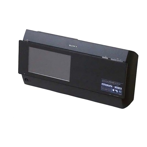
Photo: HCD-SLK20D
Model Name Using Similar Mechanism
Mechanism Type
Optical Pick-up Name
SPECIFICATIONS
Supported file format
Media type
and file
DATA CD/DATA DVD
USB device
format
1)
1)
Audio
MP3
(MPEG 1 Audio
MP3
(MPEG 1 Audio Layer 3)
Layer 3)
File extension: .mp3
File extension: .mp3
Bitrate: 32 kbps – 320 kbps, VBR
Bitrate: 32 kbps – 320 kbps,
Sampling frequencies: 32/44.1/48 kHz
VBR
DRM: Not supported
Sampling frequencies:
2)
WMA
32/44.1/48 kHz
File extension: .wma
DRM: Not supported
Bitrate: 48 kbps – 192 kbps
Sampling frequencies: 44.1 kHz
DRM: Not supported
3)
AAC
File extension: .m4a
Bitrate: 48 kbps – 320 kbps
Sampling frequencies: 44.1 kHz
DRM: Not supported
Media type
and file
DATA CD/DATA DVD
USB device
format
Video
Xvid
File extension: .avi
Video codec: Xvid video
Bitrate: 4.854 Mbps
Frame rate: 30 fps/25 fps
Resolution: 720 (width) × 480 (height) pixels/720 (width) × 576 (height) pixels
Audio codec: MP3
MPEG4
File format: MP4
File extension: .mp4/.m4v
Video codec:
MPEG4 Simple Profile (AVC is not supported.)
Bitrate: 4 Mbps
Frame rate: 30 fps
Resolution: 720 (width) × 576 (height) pixels
Audio codec: AAC-LC (HE-AAC is not supported.)
DRM: Not supported
Chinese Model
Brazilian Model
Singapore Model
"Memory Stick"
Media type
media/SD memory
and file
DATA CD/DATA DVD
card
format
Image
JPEG
Image format: Interlace or progressive format, DCF conformity, 24-bit RGB
color
File extension: .jpg/.jpeg
Resolution:
8 (width) × 8 (height) pixels (MIN) – 3,071 (width) × 2,047 (height) pixels
4)
(MAX)
1)
MP3 PRO format is not supported.
2)
WMA Lossless and WMA PRO formats are not supported.
3)
Copyright-protected AAC files and AAC Lossless format are not supported.
4)
Less than 2,000,000 pixels for progressive JPEG format.
Design and specifications are subject to change without notice.
Standby power consumption: 0.5 W
DVD RECEIVER
E Model
HCD-SLK20D
Thai Model
HCD-SLK10D
NEW
CDM86S-DVBU101
KHM-313CAB
"Memory Stick"
USB device
media/SD memory
card
Advertisement
Table of Contents

Related Manuals for Sony HCD-SLK20D


Summary of Contents for Sony HCD-SLK20D
- Page 1 • HCD-SLK10D is the amplifi er, USB, memory card, disc player and tuner section in WHG-SLK10D. Photo: HCD-SLK20D • HCD-SLK20D is the amplifi er, USB, memory card, disc player and tuner section in WHG-SLK20D. Model Name Using Similar Mechanism Mechanism Type...
- Page 2 Do not touch the soldering iron on the same conductor of the WHOSE PART NUMBERS APPEAR AS SHOWN IN THIS circuit board (within 3 times). MANUAL OR IN SUPPLEMENTS PUBLISHED BY SONY. • Be careful not to apply force on the conductor when soldering or unsoldering.
-
Page 3: Table Of Contents
HCD-SLK10D/SLK20D TABLE OF CONTENTS SERVICING NOTES 5-5. Block Diagram - VIDEO Section - ......... 35 ..........5-6. Block Diagram - POWER SUPPLY Section - ....36 5-7. Printed Wiring Boards - DMB19 Section (1/2) - .... 38 DISASSEMBLY 5-8. Printed Wiring Board - DMB19 Section (2/2) - ..... 39 2-1. -
Page 4: Servicing Notes
Model Part No. Ordinary soldering irons can be used but the iron tip has to be HCD-SLK20D: 120V AC area in E, applied to the solder joint for a slightly longer time. 4-281-621-0[] Chilean and Peruvian models... - Page 5 HCD-SLK10D/SLK20D NOTE OF THE OPERATION CONFIRMING When you confi rm the operation of this unit that has been disas- sembled, confi rm operation after connecting the FAN motor with MAIN board. This unit enters the state of protecting if the power supply of this unit is turned on without connecting the FAN motor.
- Page 6 HCD-SLK10D/SLK20D DMB19 BOARD (SIDE A) SERVICE POSITION Note: Do not insert the wire (flat type) in the same amount of connector by mistake. Refer to “2-21. HOW TO BEND WIRE (FLAT TYPE)” (page 24) and “5-1. FLAME PRINTED WIRING BOARDS” (page 31) for details. insulating sheet DMB19 board FAN motor...
- Page 7 HCD-SLK10D/SLK20D DVD MECHANISM DECK, DISPLAY BOARD (SIDE A) SERVICE POSITION Note: Do not insert the wire (flat type) in the same amount of connector by mistake. DVD mechanism deck Refer to “2-21. HOW TO BEND WIRE (FLAT TYPE)” (page 24) and “5-1. (CDM86S-DVBU101) FLAME PRINTED WIRING BOARDS”...
- Page 8 HCD-SLK10D/SLK20D TOUCH PANEL BOARD SERVICE POSITION Note: Do not insert the wire (flat type) in the same amount of connector by mistake. Refer to “2-21. HOW TO BEND WIRE (FLAT TYPE)” (page 24) and “5-1. FLAME PRINTED WIRING BOARDS” (page 31) for details. LCD module LOGO board DVD mechanism deck...
-
Page 9: Disassembly
HCD-SLK10D/SLK20D SECTION 2 DISASSEMBLY • This set can be disassembled in the order shown below. 2-1. DISASSEMBLY FLOW 2-2. TOP PANEL ASSY 2-21. HOW TO BEND WIRE (FLAT TYPE) (Page 10) (Page 24) 2-3. PANEL BACK (Page 10) 2-4. CHASSIS BLOCK (Page 11) 2-5. -
Page 10: Top Panel Assy
HCD-SLK10D/SLK20D Note: Follow the disassembly procedure in the numerical order given. 2-2. TOP PANEL ASSY 4 top panel assy 1 four screws (BVTP3 u 8) 3 two craws 3 three craws – Rear side view – 2-3. PANEL BACK 5 screw 3 screw 8 two screws (BVTP3 u 8) -
Page 11: Chassis Block
HCD-SLK10D/SLK20D 2-4. CHASSIS BLOCK ‡ 3ower ForG VettiQJ filter clamp 30 ± 5 mm (ferrite core) cord bushing tape ‡ :ire VettiQJ 9 three flat head screws (TP) 5 two screws 8 three screws (BVTP2.6) (BVTP3 u 8) 7 three flat head screws (TP) tuner (FM/AM) (TU1) 0 chassis block... -
Page 12: Dmb19 Board Block-1
HCD-SLK10D/SLK20D 2-5. DMB19 BOARD BLOCK-1 Note 2: Before disconnecting the wire (fl at type) (24 core) of optical pick-up block, solder the short-land. 3 flexible flat cable (5 core) 1 Solder the short-land. (CN4601) 4 connector 2 flexible flat cable (5 core) (CN601) (CN1107) 5 flexible flat cable 24P... -
Page 13: Dmb19 Board Block-2
HCD-SLK10D/SLK20D 2-6. DMB19 BOARD BLOCK-2 Note 4: Do not insert the wire (flat type) in the same amount of Note 3: When you install the wire (flat type), please connector by mistake. Refer to “2-21. HOW TO BEND install them correctly. WIRE (FLAT TYPE)”... -
Page 14: Holder (Jack) Block
HCD-SLK10D/SLK20D 2-8. HOLDER (JACK) BLOCK 4 connector 6 screw (SLK10D: CN601/ (BVTP2.6) SLK20D: CN603) 1 Lift up the lead pin. Note 2: When you install the wire (flat type), please install them correctly. There is a possibility that this machine damages 5 connector 7 holder (jack) block when not correctly installing it. -
Page 15: Md Block
HCD-SLK10D/SLK20D 2-9. MD BLOCK 3 MD block Note 3: When you install the wire (flat type), please Note 2: When you installing the cover (CDM) install them correctly. block, match the position of three There is a possibility that this machine damages ditches. -
Page 16: Switching Regulator (Swr1)
HCD-SLK10D/SLK20D 2-11. SWITCHING REGULATOR (SWR1) 1 two screws (BVTP3 u 8) Note: When you install the shield case (power), confirm the position of the ditch. 3 shield case (power) 4 connector (CN2) 6 switching regulator (SWR1) 5 power cord connector (CN1) –... -
Page 17: Display Board Block
HCD-SLK10D/SLK20D 2-12. DISPLAY BOARD BLOCK 4 four screws (BVTP2.6) 8 DISPLAY board block 2 connector (CN900) 7 wire (flat type) (11 core) (CN408) 6 wire (flat type) (9 core) (CN606) 1 Lift up the lead pin. 3 LCD flexible board (CN406) –... -
Page 18: Display Board
HCD-SLK10D/SLK20D 2-13. DISPLAY BOARD Note 1: When you install the wire (flat type), please install them correctly. There is a possibility that this machine damages when not correctly installing it. 2 holder (PWB DISPLAY) Insert is straight Insert is incline. to the interior. -
Page 19: Main Board-1
HCD-SLK10D/SLK20D 2-14. MAIN BOARD-1 Note 4: Do not insert the wire (flat type) in the same amount of Note 3: When you install the wire (flat type), please connector by mistake. Refer to “2-21. HOW TO BEND install them correctly. WIRE (FLAT TYPE)”... -
Page 20: Main Board-2
HCD-SLK10D/SLK20D 2-15. MAIN BOARD-2 4 Lift up the lead pin. 2 three screws 8 heat sink (AMP) (BVTP3 u 8) 2 three screws (BVTP3 u 8) 5 connector ‡ :ire VettiQJ (CN901) MAIN board 6 cushion (FPC) 9 MAIN board 1 connector (CN241) 7 two screws... -
Page 21: Touch Panel Board
HCD-SLK10D/SLK20D 2-17. TOUCH PANEL BOARD 1 five screws (BVTP2.6) 5 wire (flat type) (11 core) 3 holder (sensor) (CN801) Note 2: When you insert the wire (flat type) (11 core) in CN801 on TOUCH PANEL board, it is not necessary to make a mistake in the terminal side of the wire (flat type) (11 core). -
Page 22: Dvd Mechanism Deck (Cdm86S-Dvbu101)
HCD-SLK10D/SLK20D 2-18. DVD MECHANISM DECK (CDM86S-DVBU101) 1 two screws (BVTP3 u 8) 1 two screws (BVTP3 u 8) 2 cover (CDM) 86S block Note 2: When you install the flexible flat cable, please install them correctly. There is a possibility that this machine damages when not correctly installing it. -
Page 23: Optical Pick-Up Block (Khm-313Cab)
HCD-SLK10D/SLK20D 2-19. OPTICAL PICK-UP BLOCK (KHM-313CAB) 1 four insulator screws 4 insulator 3 connector 4 insulator 4 insulator 5 optical pick-up block (KHM-313CAB) 4 insulator – DVD mechanism deck block bottom view – 2-20. BELT (MOT) 1 belt (MOT) – DVD mechanism deck block bottom view –... -
Page 24: How To Bend Wire (Flat Type)
HCD-SLK10D/SLK20D 2-21. HOW TO BEND WIRE (FLAT TYPE) ‡ ZLUH IODW W\SH FRUH OHQJWK PP 5HI 1R The lower side is contact side. tuner (FM/AM) (TU1) 5 mm The upper side is contact side. MAIN board 40 mm (CN302) 60 mm The lower side KEY_LEFT board is contact side. - Page 25 HCD-SLK10D/SLK20D ‡ IOH[LEOH IODW FDEOH FRUH OHQJWK PP 5HI 1R DMB19 board (CN1107) The lower side is contact side. 71 mm ‡ ZLUH IODW W\SH FRUH OHQJWK PP 5HI 1R 120 mm DISPLAY board (CN606) The upper side is contact side. 155 mm 80 mm The lower side...
-
Page 26: Test Mode
DISC ANTITHEFT LOCK 5 Model name: This mode is used to unable to take sample disc out of disc slot in 00: HCD-SLK10D the shop. 16: HCD-SLK20D Procedure: 1. Press the [ ] button to turn on the system. Releasing method: 2. - Page 27 HCD-SLK10D/SLK20D DVD COLOR SYSTEM CHANGE (Except 120V AC area 1. HOW TO ENTER THE DVD SERVICE MODE in E, Mexican, Chilean, Peruvian and Brazilian models) Procedure: This mode let you change the color system of the video output 1. Press the [ ] button to turn on the system.
- Page 28 HCD-SLK10D/SLK20D • Error Code 5. Wait until a hexadecimal number appear. Emg. History Check Manual Adjust 1. Track Balance Adjust: Laser Hours 999h 59min 999h 59min 2. Track Gain Adjust: 3. Focus Balance Adjust: 01. 01 05 04 04 00 92 46 00 4.
-
Page 29: Electrical Check
HCD-SLK10D/SLK20D SECTION 4 ELECTRICAL CHECK 1-2-2. Clear the Emergency History FM TUNE LEVEL CHECK Press [DVD TOP MENU] button and then press [CLEAR] button signal on the remote commander. The error code for all emergency his- generator tory would be reset. unit Emg. - Page 30 HCD-SLK10D/SLK20D MEMO...
-
Page 31: Diagrams
HCD-SLK10D/SLK20D SECTION 5 DIAGRAMS 5-1. FRAME PRINTED WIRING BOARDS DISPLAY BOARD (SIDE B) PRO/SD DISPLAY BOARD (SIDE A) CN401 CN402 CN405 VIDEO/SAT AUDIO IN DVD VIDEO OUT VIDEO IN DMB19 BOARD J701 J704 CN1109 CN1105 CN101 CN105 (NC) CN705 MS-214 CN202 BOARD JACK BOARD... -
Page 32: Block Diagram - Servo Section
HCD-SLK10D/SLK20D 5-2. BLOCK DIAGRAM - SERVO Section - OPTICAL PICK-UP BLOCK (KHM-313CAB) RFIP RFIN AUDIO D/A CONVERTER VOA/A RF_C IC4602 VOB/B RF_B VOC/C RF_A ASDATA0 1 SDATA AOUT-L DVD_L_OUT (Page 34) VOD/D RF_D ACLK 4 MCLK AOUT-R R-CH VOE/E+G RF_F ABCK 2 SCLK VOF/F+H... -
Page 33: Block Diagram - Dsp Section
HCD-SLK10D/SLK20D 5-3. BLOCK DIAGRAM - DSP Section - CN402 B+ SWITCH PRO/SD IC406 DC_3.3V R-ch is omitted due to same as L-ch. 5 VOUT SIGNAL PATH SD/MMC-4 (VCC) 34 Card Vcc OverCurrent DET : MEMORY CARD : USB CARD VCC ENABLE SD/MS INS AUDIO SD#WP... -
Page 34: Block Diagram - Audio Output Section
HCD-SLK10D/SLK20D 5-4. BLOCK DIAGRAM - AUDIO OUTPUT Section - A/D CONVERTER, DIGITAL AUDIO PROCESSOR DIGITAL POWER AMP IC300 IC500 TB601 60 LINEIN7L PWM3_RD 8 4 INPUT_A OUT_A L.P.F. (Page 32) DVD_L_OUT OUT_A FRONT L L.P.F. PWM3_RI 9 5 INPUT_B OUT_B OUT_B OVER LOAD (Page 33) -
Page 35: Block Diagram - Video Section
HCD-SLK10D/SLK20D 5-5. BLOCK DIAGRAM - VIDEO Section - DISPLAY CONTROLLER IC401 (2/2) J701 (2/2) LCD901 VIDEO AMP DVD VIDEO OUT LIQUID CRYSTAL IC603 DISPLAY MODULE VIDEO SELECTOR LCD R0 - LCD R7 DR0 - 7 IC602 VIDEO AMP CVBS 12 D3 (DVD) IC607 VIDEO A/D CONVERTER (Page 32) -
Page 36: Block Diagram - Power Supply Section
Q261 D200 D909 B+ SWITCH EVER+3.3V REGULATOR Q905 - 907 IC908 D908 PVDD D1000, 1001 LED DRIVE SONYLOGO LED /AC-CUT (SONY LOGO) Q1000 RESET RESET SIGNAL SWITCH RESET AC-DET GENERATOR Q202 Q201 P . CONT P . CONT PROTECT PROTECT-INT... - Page 37 HCD-SLK10D/SLK20D THIS NOTE IS COMMON FOR PRINTED WIRING BOARDS AND SCHEMATIC DIAGRAMS. • Circuit Boards Location (In addition to this, the necessary note is printed in each block.) For Printed Wiring Boards. For Schematic Diagrams. Note: Note: • X : Parts extracted from the component side. •...
-
Page 38: Printed Wiring Boards - Dmb19 Section (1/2)
HCD-SLK10D/SLK20D 5-7. PRINTED WIRING BOARDS - DMB19 Section (1/2) - • See page 37 for Circuit Boards Location. • : Uses unleaded solder. (Page 49) (Page 49) MAIN BOARD MAIN BOARD CN901 CN305 DMB19 BOARD (SIDE A) JL007 CN4601 CN601 JL010 JL002 ET003... -
Page 39: Printed Wiring Board - Dmb19 Section (2/2)
HCD-SLK10D/SLK20D 5-8. PRINTED WIRING BOARD - DMB19 Section (2/2) - • See page 37 for Circuit Boards Location. • : Uses unleaded solder. DMB19 BOARD (SIDE B) C4623 C610 R4834 FL604 C502 FB608 FB607 FL603 FB603 C233 R234 R220 IC4602 C211 R233 C215... -
Page 40: Schematic Diagram - Dmb19 Section (1/4)
HCD-SLK10D/SLK20D 5-9. SCHEMATIC DIAGRAM - DMB19 Section (1/4) - • See page 56 for IC Block Diagrams. DMB19 BOARD (1/4) DGND DMB19 (Page DVDD3.3V BOARD (4/4) DVDD5V IOPMON SPFG (Page DMB19 BOARD VREFO (3/4) RF+3.3V C199 CN101 4700p JL1101 GND (LD) JL1102 DVD_LD LD (650) -
Page 41: Schematic Diagram - Dmb19 Section (2/4)
HCD-SLK10D/SLK20D • See page 56 for waveforms. • See page 61 for IC Pin Function Description. 5-10. SCHEMATIC DIAGRAM - DMB19 Section (2/4) - DMB19 DMB19 BOARD (2/4) BUS2 BOARD (4/4) (Page 43) BUS1 CN1107 DISPLAY DGND BOARD (3/3) R1257 DGND CN605 JL1220... -
Page 42: Schematic Diagram - Dmb19 Section (3/4)
HCD-SLK10D/SLK20D 5-11. SCHEMATIC DIAGRAM - DMB19 Section (3/4) - • See page 56 for IC Block Diagrams. DMB19 BOARD (3/4) DVDD3.3V DMB19 R223 100k BOARD DVDD5V 0.5% (4/4) DGND (Page 43) R225 R234 100k R232 0.5% IOPMON 0.5% REG02 R231 REG01 FCS- 0.5%... -
Page 43: Schematic Diagram - Dmb19 Section (4/4)
HCD-SLK10D/SLK20D 5-12. SCHEMATIC DIAGRAM - DMB19 Section (4/4) - • See page 56 for IC Block Diagrams. DMB19 BOARD (4/4) DVDD5V DVDD5V DMB19 DMB19 BOARD DGND DGND BOARD (1/4) (3/4) DVDD3.3V DVDD3.3V (Page 40) (Page 42) JL017 C604 CN601 JL001 (NC) JL002 C611... -
Page 44: Printed Wiring Board - Display Board
HCD-SLK10D/SLK20D 5-13. PRINTED WIRING BOARD - DISPLAY Board - • See page 37 for Circuit Boards Location. • : Uses unleaded solder. CN401 DISPLAY BOARD (CHASSIS) (CHASSIS) (Page 38) (SIDE B) DMB19 BOARD D405 R581 CN1105 DISPLAY BOARD C405 (SIDE A) ET402 CN402 JL512... -
Page 45: Schematic Diagram - Display Board (1/3)
HCD-SLK10D/SLK20D 5-14. SCHEMATIC DIAGRAM - DISPLAY Board (1/3) - • See page 56 for waveforms. • See page 61 for IC Pin Function Description. DISPLAY BOARD (1/3) CN406 R595 47k JL539 FB406 C491 DITHB VCOM C471 R546 R586 0.047 JL542 RESET JL545 AVDD... -
Page 46: Schematic Diagram - Display Board (2/3)
HCD-SLK10D/SLK20D 5-15. SCHEMATIC DIAGRAM - DISPLAY Board (2/3) - • See page 56 for waveforms. DISPLAY BOARD (2/3) CN402 PRO/SD JL479 SD-9(DAT2) JL473 JL471 SD/MMC-1(DA T3) JL474 JL475 SCLK JL472 SD/MMC-2(CMD) DA T A3 JL480 JL476 SD/MMC-3(GND) DA T A2 SD/MMC-4(VCC) JL477 SDIO/DAT A0... -
Page 47: Schematic Diagram - Display Board (3/3)
HCD-SLK10D/SLK20D 5-16. SCHEMATIC DIAGRAM - DISPLAY Board (3/3) - • See page 56 for waveforms. • See page 56 for IC Block Diagrams. DISPLAY BOARD (3/3) R821 IC B/D IC607 CN604 FB604 IC607 NJM2505AF(TE2) JL703 VIDEO AMP VIDEO_IN R814 JL702 IC B/D IC603 VOUT... -
Page 48: Printed Wiring Board - Main Section (1/2)
HCD-SLK10D/SLK20D 5-17. PRINTED WIRING BOARD - MAIN Section (1/2) - • See page 37 for Circuit Boards Location. • : Uses unleaded solder. MAIN BOARD (COMPONENT SIDE) R594 C411 R407 R400 C507 Q412 R315 R658 C640 C639 C396 C392 R310 R401 R388 R417... -
Page 49: Printed Wiring Boards - Main Section (2/2)
HCD-SLK10D/SLK20D 5-18. PRINTED WIRING BOARDS - MAIN Section (2/2) - • See page 37 for Circuit Boards Location. • : Uses unleaded solder. (Page 44) (Page 44) (Page 38) DISPLAY BOARD DISPLAY BOARD DMB19 BOARD CN408 CN606 CN4601 MAIN BOARD (CONDUCTOR SIDE) (CHASSIS) (CHASSIS) -
Page 50: Schematic Diagram - Main Section (1/4)
HCD-SLK10D/SLK20D 5-19. SCHEMATIC DIAGRAM - MAIN Section (1/4) - • See page 56 for IC Block Diagrams. MAIN BOARD (1/4) R669 R670 C649 Q609 100k 100k ISA1602AM1-T111-1EF 14.7 14.7 R668 JL670 JL671 Q608 100k ISA1602AM1-T111-1EF 14.7 14.7 R564 R556 R555 R673 R671 Q620... -
Page 51: Schematic Diagram - Main Section (2/4)
HCD-SLK10D/SLK20D 5-20. SCHEMATIC DIAGRAM - MAIN Section (2/4) - • See page 56 for waveforms. • See page 61 for IC Pin Function Description. MAIN BOARD (2/4) 92_VACS R339 R348 81_DSP-RESET R338 80_DSP-MUTE MAIN BOARD 78_DSP-CLK (3/4) 77_DSP-DA T A (Page 52) C340 C341... -
Page 52: Schematic Diagram - Main Section (3/4)
HCD-SLK10D/SLK20D 5-21. SCHEMATIC DIAGRAM - MAIN Section (3/4) - • See page 56 for waveforms. • See page 61 for IC Pin Function Description. MAIN BOARD (3/4) 54_PROTECT_AMP 54_PROTECT_AMP 73_/SD 73_/SD 56_FR/CLIP 56_FR/CLIP 55_READY 55_READY 53_/OTW2 53_/OTW2 CN107 MAIN 52_/OTW1 BOARD 52_/OTW1 JL128... -
Page 53: Schematic Diagram - Main Section (4/4)
HCD-SLK10D/SLK20D 5-22. SCHEMATIC DIAGRAM - MAIN Section (4/4) - • See page 56 for IC Block Diagrams. MAIN BOARD (4/4) (Page 52) MAIN 0_AC-DET BOARD 60_P-CONT (3/4) D+12V IC B/D P-GND 82_DVD_MONITOR (Page MAIN MAIN BOARD BOARD PVDD 66_USB_POWER (1/4) IC901 (3/4) 67_MTK_POWER... -
Page 54: Printed Wiring Boards - Panel Section
MAIN BOARD (RED) CN105 (Page 49) D1000, 1001 LOGO BOARD (CONDUCTOR SIDE) LOGO BOARD (COMPONENT SIDE) JL1001 CN1001 Q1000 (Page D1000, 1001 MAIN BOARD D1001 D1000 C1001 C1002 CN107 (SONY LOGO) JL1004 R1000 R1001 JL1003 1-883-943- (11) 1-883-943- (11) HCD-SLK10D/SLK20D... -
Page 55: Schematic Diagram - Panel Section
FRONT R- CN604 (Page 50) FRONT R- (SLK20D) BUZZER BOARD KEY_LEFT BOARD KEY_RIGHT BOARD LOGO BOARD D1000, 1001 CN703 CN706 CN261 CN262 CN263 CN1001 (SONY LOGO) JL1004 R265 R268 DGND R1000 2.2k JL731 JL268 JL290 JL1003 D1000 RESET RESET KEY1 KEY1... - Page 56 HCD-SLK10D/SLK20D • Waveforms • IC Block Diagrams – DMB19 Board – – MAIN Board – – DMB19 Board – IC201 FAN8036L IC105, 107 TK11133CSCL-G IC101 9 (XTALI) IC300 ih (XTAL_OUT) 47 46 42 41 40 39 38 37 OVER HEAT & OVER CURRENT PROTECTION 1 Vp-p...
- Page 57 HCD-SLK10D/SLK20D – DISPLAY Board – IC405 TS3USB221RSER IC406 BD2220G-TR REGULATOR VOUT EN (/EN) 1D– 2 2D+ 3 2D– 4 D– CONTROL SWITCH IC407 TPS2553DBVR RREVERSE VOLTAGE COMPARATOR – CURRENT IN 1 6 OUT SENSE 4-ms DEGLITCH CHARGE GND 2 PUMP CURRENT EN 3 DRIVER...
- Page 58 HCD-SLK10D/SLK20D IC605 TVP5150AM1PBSR 32 31 30 29 27 26 25 24 VSYNC/PALI SYNC PROCESSOR 23 FID/GLCO 22 SDA HOST PROCESSOR INTERFACE 21 SCL 20 DVDD MACROVISION DETECTION 19 DGND AIP1A AIP1B VBI/ PLL_AGND SEPARATION DATA SLICER PLL_AVDD CHROMINANCE LUMINANCE PROCESSING PROCESSING XTAL1/OSC LINE AND...
- Page 59 HCD-SLK10D/SLK20D – MAIN Board – IC500 TAS5612APHDR OC_ADJ 1 RESET 2 C_STARTUP 3 ANALOG TIMING GATE- LOOP CONTROL RECEIVER CONTROL DRIVE INPUT_A 4 – FILTER GND_A GND_B GND_B ANALOG OUT_B TIMING GATE- LOOP CONTROL RECEIVER CONTROL DRIVE INPUT_B 5 – OUT_B FILTER PVDD_B...
- Page 60 HCD-SLK10D/SLK20D IC900, 901 SI-8008TFEK IC902 SI-8001FFEK OVERCURRENT OVERCURRENT ON/OFF ON/OFF PREG PREG PROTECTION PROTECTION SOFT SOFT START START LATCH LATCH OSCILLATOR RESET OSCILLATOR RESET & & DRIVER DRIVER COMPARATOR COMPARATOR – – THERMAL THERMAL PROTECTION PROTECTION – – ERROR AMP ERROR AMP REFERENCE REFERENCE...
- Page 61 HCD-SLK10D/SLK20D • IC Pin Function Description DMB19 BOARD IC101 CXD9970R (LE) (RF AMP, SERVO DSP, DVD/CD DECODER) Pin No. Pin Name Description RF_A RF main beam (A) input from the optical pick-up block RF_B RF main beam (B) input from the optical pick-up block RF_C RF main beam (C) input from the optical pick-up block RF_D...
- Page 62 HCD-SLK10D/SLK20D Pin No. Pin Name Description CAS# Column address strobe signal output to the SD-RAM RAS# Row address strobe signal output to the SD-RAM Bank address signal output to the SD-RAM DVSS18 Ground terminal Bank address signal output to the SD-RAM 81 to 83 RA10, RA0, RA1 Address signal output to the SD-RAM...
- Page 63 HCD-SLK10D/SLK20D DISPLAY BOARD IC401 AML6226D (AUDIO DSP, DISPLAY CONTROLLER) Pin No. Pin Name Description USBA_ID Not used USBA_VBUS VBUS (for USB connector) detection signal input terminal USB VDD3.3 Power supply terminal (+3.3V) USBA D+ Two-way USB data (+) bus with the USB connector USBA D–...
- Page 64 HCD-SLK10D/SLK20D Pin No. Pin Name Description VDD1.2 Power supply terminal (+3.3V) M1 SCS0 n Chip select signal output to the SD-RAM 76, 77 M1 BA0 n, M1 BA1 n Bank address signal output to the SD-RAM DVSS Ground terminal M1 A10, 79 to 83 Address signal output to the SD-RAM M1 A3 to M1 A0...
- Page 65 HCD-SLK10D/SLK20D Pin No. Pin Name Description 155 to LCD B0 to LCD B7 RGB (blue) signal output to the liquid crystal display module VDD1.2 Power supply terminal (+1.2V) VDD3.3 Power supply terminal (+3.3V) LCD SCL(SPI) Not used LCD DCLK Data clock signal output to the liquid crystal display module LCD HSYNC Not used LCD DE...
- Page 66 Busy signal output to the servo DSP TP BUZZER Buzzer signal output terminal XIFCS Chip select signal output to the servo DSP SONYLOGO LED LED drive signal output terminal for SONY logo indicator “H”: LED on IIC-CLK Two-way I2C clock bus terminal Not used IIC-DATA...
- Page 67 HCD-SLK10D/SLK20D Pin No. Pin Name Description LED drive signal output terminal for ON/STANDBY indicator STBY-LED “L”: red LED on (STANDBY), “H”: green LED on (ON) P.CONT Power on/off control signal output to the switching regulator “H”: power on FAN-CONTROL Fan motor drive signal output terminal “H”: motor on Power supply terminal (+3.3V) PROTECT FAN...
- Page 68 HCD-SLK10D/SLK20D MAIN BOARD IC300 CXD9926ATQ (A/D CONVERTER, DIGITAL AUDIO PROCESSOR) Pin No. Pin Name Description DVDD_PWM2 Power supply terminal (+3.3V) Not used PWM2_RD, 2, 3 Digital audio signal output terminal Not used PWM2_RI 4, 5 PWM3_LD, PWM3_LI Digital audio (R-ch) signal output to the digital power amplifi er DVSS_PWM3 Ground terminal DVDD_PWM3...
- Page 69 HCD-SLK10D/SLK20D Pin No. Pin Name Description LINEIN8R Analog audio (R-ch) signal input from the iPod and USB connector AVDD_LI3 Power supply terminal (+3.3V) LINEIN9L Analog audio (L-ch) signal input from the AUDIO IN jack LINEIN9R Analog audio (R-ch) signal input from the AUDIO IN jack AVSS_LI2 Ground terminal LINEIN10L...
-
Page 70: Exploded Views
HCD-SLK10D/SLK20D SECTION 6 EXPLODED VIEWS Note: • -XX and -X mean standardized parts, so • Abbreviation The components identifi ed by mark 0 they may have some difference from the : Brazilian model or dotted line with mark 0 are critical for original one. -
Page 71: Back Panel Section
HCD-SLK10D/SLK20D 6-2. BACK PANEL SECTION • Rear side view DMB19 board section not supplied M601 not supplied not supplied supplied supplied not supplied not supplied Ref. No. Part No. Description Remark Ref. No. Part No. Description Remark 4-182-889-01 SCREW (HOOK) 4-198-670-01 SCREW, FLATHEAD (TP) 3-087-053-01... -
Page 72: Dmb19 Board Section
HCD-SLK10D/SLK20D 6-3. DMB19 BOARD SECTION • Rear side view not supplied not supplied not supplied (TERMINAL board) not supplied DISPLAY board section not supplied not supplied (JACK board) supplied supplied not supplied not supplied cover (CDM) section not supplied not supplied Ref. -
Page 73: Display Board Section
HCD-SLK10D/SLK20D 6-4. DISPLAY BOARD SECTION • Rear side view not supplied MAIN board section power block section not supplied not supplied not supplied not supplied not supplied not supplied not supplied not supplied Ref. No. Part No. Description Remark Ref. No. Part No. -
Page 74: Power Block Section
HCD-SLK10D/SLK20D 6-5. POWER BLOCK SECTION • Rear side view (E2, E51, SP) not supplied not supplied not supplied not supplied SWR1 not supplied Ref. No. Part No. Description Remark Ref. No. Part No. Description Remark 0 202 1-500-386-11 FILTER, CLAMP (FERRITE CORE) (TH) 1-837-343-11 CORD, POWER-SUPPLY (MX) 0 202... -
Page 75: Main Board Section
HCD-SLK10D/SLK20D 6-6. MAIN BOARD SECTION • Rear side view front panel section not supplied not supplied not supplied not supplied not supplied (HP board) not supplied (HP HOLDER board) not supplied Ref. No. Part No. Description Remark Ref. No. Part No. Description Remark 3-087-053-01... -
Page 76: Front Panel Section
BUTTON (POWER) (\/1) (SLK10D) 4-269-758-11 BUTTON (EJECT) (Z, – VOL +) (SLK10D) 1-828-324-61 WIRE (FLAT TYPE) (11 CORE) (400 mm) 4-269-759-01 INDICATOR (SONY LOGO) 1-828-300-61 WIRE (FLAT TYPE) (7 CORE) (160 mm) X-2582-894-1 PANEL (SERVICE) ASSY, FRONT 1-828-293-61 WIRE (FLAT TYPE) (5 CORE) (320 mm) -
Page 77: Cover (Cdm) Section
HCD-SLK10D/SLK20D 6-8. COVER (CDM) SECTION • Rear side view DVD mechanism deck section (CDM86S-DVBU101) not supplied not supplied not supplied not supplied (BUZZER board) Ref. No. Part No. Description Remark Ref. No. Part No. Description Remark 1-838-443-11 FLEXIBLE FLAT CABLE 24P (250 mm) 7-685-646-71 SCREW +BVTP 3X8 TYPE2 IT-3... -
Page 78: Dvd Mechanism Deck Section (Cdm86S-Dvbu101)
HCD-SLK10D/SLK20D 6-9. DVD MECHANISM DECK SECTION (CDM86S-DVBU101) (including MS-214 board) not supplied (MS-214 board) not supplied (including sled motor, spindle motor) spindle motor sled motor not supplied Ref. No. Part No. Description Remark Ref. No. Part No. Description Remark A-1800-839-A CDM86 (S) ASSY (Including MS-214 board) 3-087-599-01 INSULATOR SCREW... -
Page 79: Electrical Parts List
HCD-SLK10D/SLK20D SECTION 7 BUZZER DISPLAY ELECTRICAL PARTS LIST Note: • Due to standardization, replacements in • CAPACITORS : Singapore model the parts list may be different from the uF: —F : Thai model parts specifi ed in the diagrams or the com- •... - Page 80 HCD-SLK10D/SLK20D DISPLAY Ref. No. Part No. Description Remark Ref. No. Part No. Description Remark C603 1-100-597-91 CERAMIC CHIP 0.1uF C670 1-162-916-11 CERAMIC CHIP 12PF C604 1-100-597-91 CERAMIC CHIP 0.1uF C671 1-100-597-91 CERAMIC CHIP 0.1uF C605 1-100-354-21 ELECT CHIP 220uF 6.3V C672 1-165-176-11 CERAMIC CHIP 0.047uF...
- Page 81 HCD-SLK10D/SLK20D DISPLAY Ref. No. Part No. Description Remark Ref. No. Part No. Description Remark < CONNECTOR > FB611 1-469-324-21 FERRITE, EMI (SMD) (2012) FB614 1-469-324-21 FERRITE, EMI (SMD) (2012) CN401 1-794-548-21 CONNECTOR, USB (A) ( FB615 1-500-283-11 INDUCTOR, FERRITE BEAD CN402 1-842-205-11 CONNECTOR, CARD...
- Page 82 HCD-SLK10D/SLK20D DISPLAY Ref. No. Part No. Description Remark Ref. No. Part No. Description Remark R412 1-248-311-11 RES-CHIP 1/4W R515 1-216-829-11 METAL CHIP 4.7K 1/10W R414 1-216-833-11 METAL CHIP 1/10W R517 1-216-829-11 METAL CHIP 4.7K 1/10W R415 1-216-825-11 METAL CHIP 2.2K 1/10W R519 1-216-829-11...
- Page 83 HCD-SLK10D/SLK20D DISPLAY Ref. No. Part No. Description Remark Ref. No. Part No. Description Remark R608 1-216-823-11 METAL CHIP 1.5K 1/10W R710 1-216-827-11 METAL CHIP 3.3K 1/10W R610 1-216-829-11 METAL CHIP 4.7K 1/10W R721 1-216-803-11 METAL CHIP 1/10W R611 1-216-803-11 METAL CHIP 1/10W R722 1-216-821-11...
- Page 84 HCD-SLK10D/SLK20D DISPLAY DMB19 Ref. No. Part No. Description Remark Ref. No. Part No. Description Remark < VIBRATOR > C192 1-162-970-11 CERAMIC CHIP 0.01uF X401 1-814-404-11 QUARTZ CRYSTAL UNITS (24MHz) C193 1-127-715-11 CERAMIC CHIP 0.22uF X601 1-814-406-11 QUARTZ CRYSTAL UNITS (14.31818MHz) C195 1-127-715-11 CERAMIC CHIP 0.22uF...
- Page 85 HCD-SLK10D/SLK20D DMB19 Ref. No. Part No. Description Remark Ref. No. Part No. Description Remark CN4601 1-784-857-51 CONNECTOR, FFC (LIF (NON-ZIF)) 5P R102 1-216-864-11 SHORT CHIP R103 1-218-864-11 METAL CHIP 5.1K 0.5% 1/10W < DIODE > R107 1-216-833-11 METAL CHIP 1/10W R108 1-216-857-11 METAL CHIP...
- Page 86 HCD-SLK10D/SLK20D DMB19 JACK Ref. No. Part No. Description Remark Ref. No. Part No. Description Remark R246 1-216-829-11 METAL CHIP 4.7K 1/10W RB114 1-242-963-21 RES, NETWORK 33 (1005X4) R247 1-216-821-11 METAL CHIP 1/10W RB115 1-242-963-21 RES, NETWORK 33 (1005X4) R254 1-218-863-11 METAL CHIP 4.7K 0.5%...
- Page 87 1-107-826-11 CERAMIC CHIP 0.1uF < LED > C338 1-115-872-11 ELECT 2.2uF C339 1-115-872-11 ELECT 2.2uF * D1000 6-502-466-01 LED CL-270S-WS-SD-TS (SONY LOGO) C340 1-107-826-11 CERAMIC CHIP 0.1uF * D1001 6-502-466-01 LED CL-270S-WS-SD-TS (SONY LOGO) C341 1-112-746-11 CERAMIC CHIP 4.7uF 6.3V...
- Page 88 HCD-SLK10D/SLK20D MAIN Ref. No. Part No. Description Remark Ref. No. Part No. Description Remark C342 1-107-826-11 CERAMIC CHIP 0.1uF C507 1-162-964-11 CERAMIC CHIP 0.001uF C343 1-107-826-11 CERAMIC CHIP 0.1uF C509 1-100-597-91 CERAMIC CHIP 0.1uF C344 1-126-382-11 ELECT 100uF C525 1-100-597-91 CERAMIC CHIP 0.1uF C348 1-107-826-11...
- Page 89 HCD-SLK10D/SLK20D MAIN Ref. No. Part No. Description Remark Ref. No. Part No. Description Remark C921 1-100-597-91 CERAMIC CHIP 0.1uF D528 6-501-696-01 DIODE RSA39LTE25 D538 6-501-696-01 DIODE RSA39LTE25 C922 1-126-795-11 ELECT 10uF D578 6-501-696-01 DIODE RSA39LTE25 C923 1-126-795-11 ELECT 10uF D588 6-501-696-01 DIODE RSA39LTE25 C924...
- Page 90 HCD-SLK10D/SLK20D MAIN Ref. No. Part No. Description Remark Ref. No. Part No. Description Remark L900 1-400-424-11 INDUCTOR 47uH R118 1-216-809-11 METAL CHIP 1/10W R120 1-216-833-11 METAL CHIP 1/10W L901 1-400-424-11 INDUCTOR 47uH R121 1-216-833-11 METAL CHIP 1/10W L902 1-400-424-11 INDUCTOR 47uH R122 1-216-833-11...
- Page 91 HCD-SLK10D/SLK20D MAIN Ref. No. Part No. Description Remark Ref. No. Part No. Description Remark R205 1-216-833-11 METAL CHIP 1/10W R370 1-216-835-11 METAL CHIP 1/10W R206 1-216-821-11 METAL CHIP 1/10W (EA, MX, BR, SP, TH, IND) R207 1-216-864-11 SHORT CHIP R370 1-216-838-11 METAL CHIP 1/10W...
- Page 92 HCD-SLK10D/SLK20D MAIN Ref. No. Part No. Description Remark Ref. No. Part No. Description Remark R555 1-216-791-11 METAL CHIP 1/10W R922 1-216-797-11 METAL CHIP 1/10W R556 1-216-791-11 METAL CHIP 1/10W R923 1-216-845-11 METAL CHIP 100K 1/10W R564 1-216-864-11 SHORT CHIP R924 1-216-821-11 METAL CHIP 1/10W...
- Page 93 HCD-SLK10D/SLK20D MAIN MS-214 TERMINAL TOUCH PANEL Ref. No. Part No. Description Remark Ref. No. Part No. Description Remark RB182 1-234-372-11 RES, NETWORK 100 (1005X4) 1-827-731-61 WIRE (FLAT TYPE) (11 CORE) (200 mm) RB187 1-234-372-11 RES, NETWORK 100 (1005X4) 1-828-333-61 WIRE (FLAT TYPE) (13 CORE) (320 mm) 1-838-111-21 CABLE, FLEXIBLE FLAT (5 CORE) (620 mm) <...
- Page 94 HCD-SLK10D/SLK20D REVISION HISTORY Checking the version allows you to jump to the revised page. Also, clicking the version at the top of the revised page allows you to jump to the next revised page. Ver. Date Description of Revision 2011.07...
Need help?
Do you have a question about the HCD-SLK20D and is the answer not in the manual?
Questions and answers
COMO ACTIVAR EL MODO DEMOSTRACIÓN